Note: Descriptions are shown in the official language in which they were submitted.
CA 02399374 2002-08-07
WO 01/57565 PCT/GBO1/00409
IMPROVED INTEGRATED OPTICAL DEVICE
FIELD OF INVENTION
This invention relates to an improved integrated
optical device or optoelectronic device, and particularly
to hybrid integration of devices formed in different
material systems. For example, hybrid integration of III-V
S semiconductor devices with passive waveguide structures.
BACKGROUND TO INVENTION
Hybrid integration of III-V semiconductor components
with passive waveguides is of increasing importance as a
method of increasing the functionality of integrated
optical and photonic systems. Applications include:
optical communication systems, optical sensing
applications, and optical data processing.
A fundamental problem in hybrid integration is that
the semiconductor element has a higher refractive index
than the passive waveguide. In the case of a III-V
semiconductor component integrated on a planar Silica (Si02)
platform, the refractive indices are typically around 3.6
for the semiconductor and 1.5 for the Silica. This
refractive index difference causes a number of problems, eg
there is a high reflection coefficient at the interface
between the two devices, and the mode size in each device
is different. Both of these effects result in a loss in
optical power and reduced coupling efficiency between the
two devices, and scattering of light, and undesirable
reflections.
It is an object of the present invention to obviate or
at least mitigate one or more of the aforementioned
problems in the prior art.
Further objects of various embodiments of the present
invention include:
enablement of hybrid integration to be carried out,
while ensuring good mode matching between active and
SUBSTITUTE SHEET (RULE 26)
CA 02399374 2002-08-07
WO 01/57565 PCT/GBO1/00409
2
passive sections;
ease of manufacture;
low loss coupling between active and passive sections.
SLTI~2ARY OF INVENTION
According to a first aspect of the present invention
there is provided an integrated optical device providing
first and second devices optically coupled one to the other
and formed in first and second different material systems,
at least one of the first or second devices having a
Quantum Well Intermixed (QWI) region at or adjacent a
coupling region between the first and second devices.
Quantum Well Intermixing (QWI) permits a postgrowth
modification to the absorption edge of Multiple-Quantum
Well (MQW) material, and therefore provides a flexible,
reliable, simple, and low-cost approach compared to
competing integration schemes such as selective area
epitaxy or selective etching and regrowth.
Quantum Well Intermixing (QWI) provides a means of
tuning an absorption band edge controllably in Quantum Well
(QW) structures, and may be utilized to fabricate low-loss
optical interconnects between monolithically integrated
optical devices or integrated optoelectronic devices.
The first material system may be a III-V semiconductor
material system. The III-V semiconductor material may be
selected from or include one or more of: Gallium Arsenide
(GaAs), Aluminium Gallium Arsenide (AlGaAs), Indium
Phosphide (InP), Gallium Arsenide Phosphide (GaAsP),
Aluminium Gallium Arsenide Phosphide (AlGaAsP), Indium
Gallium Arsenide Phosphide (InGaAsP), or the like.
The second material system may be a non III-V
semiconductor material. The second material system may be
selected from: Silica (SiO,), Silicon (Si), Lithium Niobate
(LiNbO;), a polymer, a glass, or the like any of which may
be doped with optically active material.
The first device may be or include an active device
component, such as a laser diode, light emitting diode
SUBSTITUTE SHEET (RULE 26)
CA 02399374 2002-08-07
WO 01/57565 PCT/GBO1/00409
3
(LED), optical modulator, optical amplifier, optical
switch, or switching element, optical detector (eg
photodiode), or the like. The first device may also include
a passive device compound such as a passive waveguide.
The second device may be or include a passive
component such as a passive waveguide.
Preferably, the coupling region provides means for at
least substantially mode matching between the first and
second devices.
In one arrangement the first device provides the
Quantum well (QW)intermixed region.
In the one arrangement the mode matching means may
comprise a waveguide provided in the first device which
waveguide may be a "tapered" waveguide providing a linear
change in width, a non-linear change in width, and/or a
"periodic" or "a-periodic" segmentation.
Preferably, the coupling region provides anti-
reflection means at or near an interface between the first
and second devices.
The anti-reflection means may comprise or include an
anti-reflection coating on a facet of the first device
provided at the interface between the first and second
devices.
The anti-reflection means may also comprise or include
facets of the first and second devices provided at the
interface between the first and second devices, the facets
being formed at an (acute) angle to an intended direction
of optical transmission. The facets may therefore be
referred to as "angled facets".
In a preferred embodiment a first waveguide section in
the first device and preferably also a second waveguide
section in the second device is/are bent.
The integrated optical device may be adapted to
operate in a wavelength region of 600 to 1300nm or of 1200
to 1700 nm.
According to a second aspect of the present invention,
there is provided an integrated optical circuit,
SUBSTITUTE SHEET (RULE 26)
CA 02399374 2002-08-07
WO 01/57565 PCT/GBO1/00409
4
optoelectronic integrated circuit, or photonic integrated
circuit including at least one integrated optical device
according to the first aspect of the present invention.
According to a third aspect of the present invention
there is provided an apparatus including at least one
integrated optical device, the at least one integrated
optical device providing first and second devices optically
coupled one to the other and formed in first and second
different material systems, one of the first or second
devices having a Quantum Well Intermixed (QWI) region at or
adjacent a coupling region between the first and second
devices.
According to a fourth aspect of the present invention
there is provided a method of providing an integrated
optical device having hybrid integration of first and
second devices formed in first and second different
material systems comprising:
providing one of the first or second devices with a
Quantum Well Intermixed (QWI) region at or adjacent a
coupling region between the first and second devices.
The Quantum Well Intermixed (QWI)region may be formed
from a number of techniques, but preferably by a universal
damage induced technique, Impurity Free Vacancy Diffusion
(IFVD).
In a preferred embodiment, the Quantum Well Intermixed
(QWI) region may be formed in the first device by
intermixing a Quantum Wells) (QW) in a core optical
guiding layer of the first device, eg by Impurity Free
Vacancy Diffusion (IFVD).
When performing IFVD upon a top cap layer of the a
III-V semiconductor material comprising the first device is
deposited a dielectric, eg SiO~ layer or film. Subsequent
rapid thermal annealing of the semiconductor material
causes bonds to break within the semiconductor alloy, eg
Gallium ions or atoms vahich ara susceptible to Silica
(SiO~), to dissolve into the Silica sc as to leave vacancies
in the cap layer. The vacancies then diffuse through the
SUBSTITUTE SHEET (RULE 26)
CA 02399374 2002-08-07
WO 01/57565 PCT/GBO1/00409
semiconductor material inducing layer intermixing, eg in
the Quantum Wells) (QW).
IFVD has been reported in "Quantitative Model for the
Kinetics of Compositional Intermixing in GaAs - AlGaAs
S Quantum - Confined Heterostructures", by Helmy et al, IEEE
Journal of Selected Topics in Quantum Electronics, Vol 4,
No 4, July/August 1998, pp 653 - 660, the content of which
is incorporated herein by reference.
According to a fifth aspect of the present invention
there is provided a first device according to the first
aspect of the present invention.
BRIEF DESCRIPTION OF DRAWINGS
Embodiments of the present invention will now be
described, by way of example only, and with reference to
the accompanying diagrams, which are:
Figure 1(a) a schematic plan view of a first
semiconductor chip integrated with a
passive photonic integrated circuit
(PIC) according to a first embodiment
of the present invention;
Figure 1(b)-(d) schematic plan views of second, third
and fourth semiconductor chips
integratable with a passive photonic
integrated circuit (PIC) similar to or
the same as that of Figure 1(a)
according to the present invention;
Figure 2(a) a schematic plan view of a fifth
semiconductor chip according to the
present invention;
Figure 2(b) a schematic plan view of the fifth
semiconductor chip of Figure 2(a)
integrated with a passive photonic
SUBSTITUTE SHEET (RULE 26)
CA 02399374 2002-08-07
WO 01/57565 PCT/GBO1/00409
6
integrated circuit (PIC) according to
a fifth embodiment of the present
invention;
Figure 3 a schematic cross-sectional end view
showing a possible layer structure of
a semiconductor chip according to a
sixth embodiment of the present
invention;
Figure 4 a schematic perspective view from one
end, above and to one side of the
semiconductor chip of Figure 3;
Figure 5 a schematic perspective view from one
end, above and to one side of a
semiconductor chip according to a
seventh embodiment of the present
invention.
DETAILED DESCRIPTION OF DRAWINGS
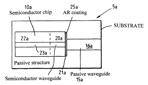
Referring initially to Figure 1(a) there is
illustrated an integrated optical device, generally
designated 5a, according to a first embodiment of the
present invention and providing the first and second
devices 10a, 15a respectively, the first and second devices
10a, 15a being optical coupled one to the other and formed
in first and second dis-similar material systems, at least
one of the first or second devices 10a, 15a having a
Quantum Well Intermixed (QWI) region 20a at or adjacent a
coupling region 21a between the first and second devices
10a,15a.
In this embodiment the first materials system is a
III-V semiconductor material system based on either Gallium
Arsenide (GaAs) or Indium Phosphide (InP). For example the
III-V semiconductor material may be selected or include one
or more of: Gallium Arsenide (GaAs), Aluminium Gallium
SUBSTITUTE SHEET (RULE 26)
CA 02399374 2002-08-07
WO 01/57565 PCT/GBO1/00409
7
Arsenide (AlGaAs), and Indium Phosphide (InP), Gallium
Arsenide Phosphide (GaAsP), Aluminium Gallium Arsenide
Phosphide (AlGaAsP), Indium Gallium Arsenide Phosphide
(InGaAsP), or the like. The integrated optical device 5a
may therefore be adapted to operate in the so-called
"short" wavelength region of 600 to 1300nm, or the so-
called "long" wavelength region of 1200 to 1700 nm.
The second material system is a non III-V
semiconductor material and can be selected from Silica
(SiO.), Silicon (Si), Lithium Niobate (LiNbo~), a polymer,
glass or the like.
The first device 10a comprises an active device
component 22a, selected from a laser diode, light emitting
diode (LED), optical modulator, optical amplifier, optical
switching element, optical detector (eg photodiode), or the
like. The active device component 22a is spaced from the
Quantum Well Intermixed (QWI) region 20a, the active device
component 22a, and passive QWI region 20a being in optical
communication one with the other via a waveguide 23a such
as a ridge waveguide.
The second device 15a in this embodiment includes a
passive device component in the form of a passive waveguide
16a.
The coupling region 21a provides anti-reflection means
at or near an interface between the first and second
devices 10a, 15a. The anti-reflection means comprise anti-
reflection coating 25a on an end facet on first device 10a
provided at the interface between the first and second
devices 10a, 15a.
In a modification the anti-reflection means may also
comprise facets of the first and second devices 10a, 15a
provided at the interface between the first and second
devices 10a, 15a, the facets being formed at an acute angle
to the intended direction of the optical transmission along
waveguides 23a, 16a. In such a modification the facets may
be referred to as "angled facets".
Referring now to Figure 1 (b) there is illustrated a
SUBSTITUTE SHEET (RULE 26)
CA 02399374 2002-08-07
WO 01/57565 PCT/GBO1/00409
8
second embodiment of a first device lOb comprising part of
an optically integrated device according to the present
invention, like parts of the device lOb being identified by
the same numerals as those for the first embodiment, but
suffixed "b". In this second embodiment the waveguide 23b
includes a curved portion 30b so as to improve optical
coupling between the first device lOb and a second device
(not shown) , by reduction of reflections at the interface
between the first device lOb and the second device.
Referring now to Figure 1(c), there is illustrated a
third embodiment of a first device, generally designated
10c, comprising part of an optically integrated device
according to an embodiment of a present invention. The
device 10(c) is similar to the device 10a of the first
embodiment, and like parts are identified by like numerals,
but suffixed "c". However, as can be seen from Figure
1(c), the waveguide 23c includes at an end adjacent the
coupling region to the second device (not shown) a tapered
region 30c which, in use, causes an optical mode "M"
transmitted along the waveguide 23c to expand as it
traverses the optical waveguide 23c and is output from the
first device lOc from the tapered region 30c . The converse
of course applies for optical coupling to the first device
lOc from the second device (not shown).
Referring now to Figure 1(d), there is shown a foi.lrth
embodiment of a first device lOd comprising part of an
optically integrated device according to an embodiment of
the present invention. The first device lOd is
substantially similar to the device 10a of the first
embodiment, like parts being identified by like numerals
but suffixed "d". However, in the first device 10d, the
waveguide 23d includes at an end adjacent a coupling region
to a second device (not shown) a curved and tapered region
30b. The first device lOd therefor=. combines the features
of the embodiments of Figures 1 (b) amd (c) .
As will be appreciated, to ele :trically control the
first devices l0a-lOd, an ele.~_trical contact (metalisation)
SUBSTITUTE SHEET (RULE 26)
CA 02399374 2002-08-07
WO 01/57565 PCT/GBO1/00409
9
will be fabricated cn a surface of the waveguide 23a-23d,
while a further electrical contact (metalisation) will be
provided on an opposing surface of the device l0a-lOb.
It will be appreciated that the modifications shown in
the second, third and fourth embodiments 10b, 10c, 10d,
seek to improve optical coupling between the first device
10b, 10c, 10d, and a second device (not shown).
It will also be appreciated that the intermixed region
20a to 20b acts to prevent, or at least reduce, optical
absorption in the intermixed region 20a-20d adjacent to the
coupling region 21a-21d. This is particularly so in the
curved tapered waveguide section 30b.
It will further be appreciated that although herein
above the waveguide sections 30c and 30d have been referred
to as "tapered" regions, the optical mode transmitted
therein towards an end of the first device lOc to lOd
adjacent to second device (not shown) actually flares.
Referring now to Figures 2(a) and (b), there is
illustrated an integrated optical device general designated
5e, according to a fifth embodiment of the present
invention. The device 5e provides first and second devices
10e, 15e optical coupled one to the other and formed in
first and second different material systems, the first
device 10e having a Quantum Well Intermixed (QWI) region
20e adj acent a coupling region 21e between the f first and
second device 10e, 15e. As can be seen from Figures 2(a)
and (b) a waveguide 23e of the first device 10e comprises
a tapered curved region 30e adjacent a coupling region 21e
between the first and second devices 10e, 15e. Further, an
anti-reflection coating 25e is provided within the coupling
region 21e on an end facet of the first device 10e. Also,
a passive waveguide 16e of the second device 15e is
complementarily curved to the portion 30e so as to also
assist in optical coupling between the first and second
devices 10e, 15e.
Referring now to Figures 3 and 4, there is illustrated
a sixth embodiment of a first device generally designated
SUBSTITUTE SHEET (RULE 26)
CA 02399374 2002-08-07
WO 01/57565 PCT/GBO1/00409
lOf according to the present invention. Like parts of the
device lOf are identified by the same numerals as for the
device 10a of the first embodiment of Figure 1(a), but
suffixed "f".
5 The device lOf comprises an GaAs substrate 50f, upon
which are grown a number of epitaxial layers by known
growth technique such as Molecular Beam Epitaxy (MBE) or
Metal Organic Chemical Vapour Deposition (MOCVD). The
layers comprise a first 0.5~.m to l~,m n-doped Alo.soGao.soAs
10 layer 55f, a second 5~m n-doped Alo,4oGao.EOAs layer 60f, a
third 0.5~cm substantially intrinsic Alo.~oGao.eoAs core layer,
including a lOnm GaAs Quantum Well (QW), 70f as grown. On
the core layer 65f is grown a l~,m p-doped Al~,_QOGao.6oAs layer
75f, and finally on that layer is grown a p+ doped GaAs
capping contact layer 80f. As can be seen from Figure 3,
a ridge waveguide 23f is formed in the layers 75f,80f by
known photolithographic techniques. Further in this
embodiment, a second broader ridge or mesa 35f is also
formed in the layers 65f and 60f. Thus the ridge waveguide
23f comprises a primary waveguide while the mesa 35f
comprises a secondary waveguide. The device lOf also
includes a tapered region 30f on the waveguide 23f. The
device 10f, therefore, acts as a mode converter converting
a mode from the device lOf coupled to a second device (not
shown), or a mode transmitted from the second device to the
first device 10f.
As can be seen from Figure 3, contact metallisations
40f and 45f may be provided on a top of ridge 23f and an
opposing surface of the substrate 50f. Further, as can be
seen from Figure 4, the device lOf includes a Quantum Well
Intermixed (QWI) region 20f adjacent to the end of the
device corresponding to the tapered region 30f.
In this embodiment the Quantum Well Intermixed (QWI)
region 20a is formed in the first device 10f by intermixing
the Quantum Well 70f in the layer 60f within the region 20f
by Impurity Free Vacancy Diffusion (IFVD). When performing
SUBSTITUTE SHEET (RULE 26)
CA 02399374 2002-08-07
WO 01/57565 PCT/GBO1/00409
11
IFVD upon a top cap layer 80f of the III-V semiconductor
material comprising the first device 10f, there is
deposited a dielectric, eg Silica (Silo) , layer of film.
Subsequent rapid thermal healing of the semiconductor
material causes bonds to break within the semiconductor
alloy and eg Gallium ions or atoms - which are susceptible
to Silica (SiO ) - to dissoJ.ve into the Silica so as to
leave vacancies in the cap layer 80f. The vacancies then
diffuse through the semiconductor material inducing layer
intermixing, eg in the Quantum Well 70f.
Referring now to Figure 5 and to Table 1, there is
illustrated a seventh embodiment of a first device
generally designated 10g, for use in an optically
integrated device according to the present invention. In
this sixth embodiment, the first device lOg is fabricated
in Indium Gallium Arsenide Phosphide ( In Inl_;~ Ga~ Asy P1_y) .
The layer structure, grown on an Indium Phosphide
(InP) substrate 50g, is shown in Table 1 below.
SUBSTITUTE SHEET (RULE 26)
CA 02399374 2002-08-07
WO 01/57565 PCT/GBO1/00409
12
TABLE 1
Repeats Thickness Material x y Dopant Type
(A)
1 1000 In(x)GaAs 0.53 Zn p
1 500 Q1/18 Zn p
1 11500 InP p
1 50 Q1.05 i
1 2500 InP
1 800 Ql.l i
1 500 Q1.8 i
5* 120 Q1.26 i
5* 65 In (x) GaAs 0 . i
53
1 120 Q1.26 i
1 500 Q1.18 i
1 800 Ql.l i
1 50000 Q1.05 Si n
1 10000 InP (buffer Si n
layer
adjacent
substate )
* - Quantum Well (QW)structure
Q = Quaternary, eg Q1.1 - quaternary with l.l~.m bandgap
As can be seen from Figure 5, the first device lOg
includes an active waveguide 23g and adjacent to coupling
region to a second device (not shown) a tapered region 30g.
The waveguide 23g comprises a primary waveguide of the
first device 10g, while a further ridge or mesa 35g formed
on the device 10g comprises a secondary waveguide . In use,
the optical radiation generated uith:!n or transmitted from
the waveguide 23g towards the tapered region 30g as an
optical mode, is caused upon transmission through region
SUBSTITUTE SHEET (RULE 26)
CA 02399374 2002-08-07
WO 01/57565 PCT/GBOi/00409
13
30g from primary optical guiding layer 65g into layer 60g
for optical coupling to second device (not shown).
The first devices 5f,5g illustrate a design of
regrowth-free tapered waveguide coupler. The small rib
waveguide 23f,23g is located on top of a thick lower
cladding layer 60f that is partially etched to form mesa
waveguide 35f,35g. When the small rib 23f,23g is
sufficiently wide, the fundamental optical mode is confined
to the small 23f,23g, and there is a high confinement of
light within the undoped waveguide core layer 65f, (which
itself contains the active Quantum Well layers 75f or
intermixed region 20f,20g). At the other extreme, when the
small rib 23f,23g is sufficiently narrow, the fundamental
mode expands to fill the larger mesa waveguide 35f,35g.
This behaviour is a consequence of the design of the
waveguide layers. The thicknesses and compositions of the
Quantum Well layers at the top of the mesa 35f,35g, and
extending under the small rib 23f,23g are such as to
prevent guiding of light within these layers if the upper
layers comprising the small rib 23f,23g are etched away.
The resulting waveguide allows separate optimisation of the
optical mode properties of the rib 23f, 23g and mesa 35f, 35g
waveguides at the two extremes of rib width. At large rib
widths high-performance device action (such as optical
amplification, optical detection, electro-absorptive or
electro-refractive modulation) can be achieved. At small
rib widths the dimensions of the large mesa 35f,35g and
thickness of the lower cladding materials establish the
optical mode size of the mesa waveguide for optimum
coupling to passive Silica waveguides. The expanded mode
can be designed for optimum coupling directly to single
mode waveguides in the second (non-semiconductor) material
single-mode or to optical fibre, including 1.3 ~.m and 1.5
~.m telecommunication fibre.
The layer structure shown in Figure 3 would be used to
make a first device lOf with Quantum Wells resonant with
radiation at a wavelength of around 860nm. The structure
SUBSTITUTE SHEET (RULE 26)
CA 02399374 2002-08-07
WO 01/57565 PCT/GBO1/00409
14
shown in Figure 5 would be used to make a first device lOg
with Quantum Wells resonant with radiation at a wavelength
around 1 . 5 ~.m .
It will be appreciated that the embodiments of the
invention hereinbefore described are given by way of
example only, and are not meant to limit the scope thereof
in any way.
It will be particularly understood that the device of
the present invention is easier and simpler to manufacture
than other devices, and therefore provides the potential of
obtaining high quality devices at reduced cost.
It will also be appreciated that in the disclosed
embodiments the mode matching means comprised a "tapered"
waveguide providing a linear or non-linear change in width,
in modified implementations the change in width may be
"periodically" or "a-periodically" segmented.
It will further be understood that in this invention,
Quantum Well Intermixing (QWI) is used to reduce absorption
by the Quantum Well layers within the taper region and so
reduce optical losses in the taper region and improve
device efficiency.
Finally, it will be appreciated that in a modification
the first device may be inverted with respect to the second
device, ie the ridge waveguide of the first device may be
in contact with, or adjacent, a surface of the second
device.
SUBSTITUTE SHEET (RULE 26)