Note: Descriptions are shown in the official language in which they were submitted.
CA 02399642 2002-08-07
WO 01165218 PCT/GB00/00745
ELECTROMAGNETIC DETECTION APPARATUS
Technical Field
The present invention relates to electromagnetic detection apparatus, and in
particular to an
electromagnetic gauge for measuring a parameter of a sample, especially an
infrared absorption
gauge.
Background Art
Infrared absorption gauges are well known and are used for example for
measuring constituents
of samples (e.g. the moisture content of paper or tobacco, or the fat, protein
and water contents
of foodstuffs), the amounts of substances absorbed or adsorbed on a substrate,
the thickness of
coatings or films on a substrate or the degree of cure of resins in a printed
circuit board. In this
specification, the term "parameter'' is used to denote the property
(composition, coating thickness
etc.) of the sample being measured.
Infrared absorption gauges conventionally operate by projecting infrared
radiation at two or more
wavelengths onto a sample or a substrate and measuring the intensity of the
radiation reflected,
transmitted or scattered by the sample. Signals proportional to the measured
intensity are
processed to provide a value of the parameter being measured. At least one of
the two or more
wavelengths projected by the gauge is chosen to be absorbed by the parameter
of interest while at
least one other wavelength is chosen to be substantially unaffected by the
parameter of interest.
For example, when measuring the amount of water in a sample, one of the
wavelengths (the
"measuring wavelength") can be chosen at an absorption wavelength of water
(either 1.45
micrometer or 1.94 micrometer) and the other wavelength (known as the
"reference
wavelength") is chosen to be one that is not significantly absorbed by water.
Generally, gauges include an infrared radiation source having a broad emission
spectrum and a
detector for receiving radiation reflected, scattered or transmitted by the
sample; filters are
placed between the source and the sample to expose the sample only to the
desired measuring and
reference wavelengths; in this case, the sample is successively exposed to
radiation at the
selective wavelengths, e.g. by placing appropriate filters on a rotating wheel
in front of the
CA 02399642 2002-08-07
WO 01/65218 PCT/GB00/00745
2
radiation source. Alternatively, the filter wheel can be placed between the
sample and the
detector and each filter is successively interposed between the sample and the
detector.
Naturally, if the source can produce radiation of the desired wavelength
without the use of filters,
then such filters can be dispensed with.
The detector measures the intensity of light after interaction with the sample
and produces a
signal according to the intensity of the radiation incident upon it. In the
most simple case, by
calculating the ratio between the signal from the detector when receiving
light at the measuring
wavelength to that when receiving light at the reference wavelength, a signal
can be obtained that
provides a measure of the parameter concerned, for example the amount of
moisture in a sample.
Often, several measuring wavelengths and/or several reference wavelengths are
used and the
signals of the measuring wavelengths and of the reference wavelengths are used
to calculate the
parameter concerned.
The detectors which are normally used in such measuring gauges are
conventionally lead sulphide
(PbS) detectors, because they display better detectivity and wavelength
response than most other
detectors which might be employed in such applications. However, PbS detectors
have a number
of limitations, including particularly the following:
(a) Temperature sensitivity: the resistance of a typical detector cell falls
by 25 % for
every 10°C rise in temperature.
(b) Non-linearity: the response of the detector to incident radiation is not
linear over
the whole operational range of the detector.
(c) Response time: the response time of the detector usually limits the rate
at which
different wavelengths can be detected, that is the rate at which successive
filters
can be employed. Faster filter data rates tend to result in the signal from
the
wavelength obtained from one filter lagging so much that it bleeds into that
from
the wavelength obtained from the next filter, thereby causing "cross-talk".
(d) Noise: at low frequencies of operation of the detector a type of noise
known as 1/f
noise predominates. If a relatively low filter data rate is chosen to avoid
cross-
talk, then such noise becomes a problem.
CA 02399642 2005-08-15
3
It is apparent from the above that the detectors currently used in measuring
gauges
suffer from a number of drawbacks, not the least of which is their response
time.
The present invention seeks to address these problems and to improve the
performance of the detectors in electromagnetic detection apparatus, such as
infrared measuring gauges.
Disclosure of Invention
Accordingly, in one aspect of the present invention there is provided an
infrared gauge for measuring a parameter of a sample, comprising: a main
source of
infrared radiation for illuminating the sample, a detector circuit including a
detector for
detecting infrared radiation received from the sample and for generating a
signal
representing the radiation received, and means for stabilising a response
characteristic of the detector to the radiation received, said stabilising
means
comprising: a controlled source of additional infrared radiation for directing
radiation
at the detector, and means for controlling the source of additional radiation
in
dependence upon the signal generated by the detector.
CA 02399642 2005-10-20
3a
In a preferred form of the invention, the means for stabilising a response
characteristic of the detector is arranged to achieve at least one of the
following: linearization of the detector response and/or extension of the
frequency of the response of the detector.
In an infrared measuring gauge, improvement of the linearity tends to
enhance the temperature stability of the measuring gauge and lead to more
predictable calibration. Extension of the detector frequency response permits
the use of much faster filter data rates, and thus reduces the response time
of
o the measuring gauge. Faster filter speeds also result in reduced ambient
light
sensitivity and can lead to improvements in noise.
Advantageously, the means for controlling the radiation source are arranged
to adjust the intensity of the radiation emitted by this source.
CA 02399642 2002-08-07
WO 01/65218 PCT/GB00/007.15
4
In one embodiment of the invention, the controlling means are arranged to
adjust the intensity of
the radiation emitted by the radiation source in order to maintain the
detector signal at a
substantially predetermined level.
In another embodiment of the invention, the controlling means are arranged to
adjust the intensity
of the radiation emitted by the radiation source in order to minimise
variations in the detector
signal .
Advantageously, a feedback path is provided from the output of the detector
circuit to the second
radiation source for this purpose.
Brief Description
The invention is described further, by way of example, with reference to the
accompanying
drawings, in which:
Fig. 1 is a schematic section through the head of a known infrared gauge, for
the
purposes of explanation;
Fig. 2 is a detailed schematic section through a detector mounting plate of
such an
infrared gauge, but illustrating the present invention;
Fig. 3 is a block diagram showing one embodiment of the present invention;
Fig. 4 is a block diagram showing another embodiment of the present invention;
Fig. 5 is a graph showing the non-linearity of the response of a conventional
PbS
detector.
Fig. 6 is a graph representing the frequency response of a PbS detector in a
known
gauge; and
Fig. 7 is a graph showing the frequency response of a detector when the
present invention
is employed.
CA 02399642 2002-08-07
WO 01/65218 PCT/GB00/00745
Modes for carrying out the Invention
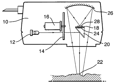
Referring initially to Fig. l, this shows the head 10 of a known infrared
gauge, for example as
described in our published PCT application no. W098/22806. The head 10
contains a lamp 12
providing a source of infrared radiation, and a circular filter wheel 14
driven by a motor 16. The
filter wheel 14 carries a series of filters, for example 5 filters, and each
filter is designed to pass
a different selected emission wavelength. The light passed by the respective
filters is directed
towards a detector mounting table 18, as described below.
The mounting table 18 carries a beam sputter 20 which reflects a portion of
the light beam
downwardly out of the infrared gauge 10 towards a sample 22. A remaining
portion of the
infrared light beam striking the beam sputter 20 is refracted within the beam
sputter towards a
detector assembly 24 including a photo-electric sensor. Meanwhile, the light
emitted by the head
towards the sample 22 is reflected back from the sample 22 towards a
collecting mirror 26 in
the head 10 and thence to another detector assembly 28 including another photo-
electric sensor.
The two detector assemblies 24, 28 thus generate detection signals
representing, respectively, the
intensity of the light emitted by the lamp 12 and filtered by a selected one
of the filters, and the
intensity of that same light after reflection from the sample 22. The detector
assembly 28 is
normally referred to as the primary detector assembly and the detector
assembly 24 is normally
referred to as the secondary detector assembly. The signals generated by the
two detector
assemblies 28, 24 are processed in a known manner to provide a measurement of
a parameter of
the sample 22.
The measuring gauge described thus far is known as a back-scatter gauge in
that the light which
is detected is scattered back from the sample whose parameter is to be
measured. Another known
measuring gauge detects the light that is transmitted through a sample whose
parameter is to be
measured
Turning now to Fig. 2, this shows a detector arrangement according to the
present invention
having a mounting table 18 bearing a primary detector assembly 28 and a
secondary detector
assembly 24 as shown in Fig. 1. As is known, the primary detector assembly 28
features a PbS
detector 282 and a blocking filter 284, which is a small sheet of silicon,
mounted in front of the
detector 282 in order to block out visible light. Likewise, the secondary
detector assembly 24
features a PbS detector 242 and a blocking filter 244, also a small sheet of
silicon, mounted in
front of the detector in order to block out visible light.
CA 02399642 2002-08-07
WO 01/65218 PCT/GB00/00745
6
In accordance with the invention, however, the mounting table 18 also bears
additional sources of
radiation, in this instance a first Gallium Arsenide (GaAs) infrared emitter
or diode 30 directed
towards the blocking filter 244 and a second GaAs diode 32 directed towards
the blocking filter
284. The GaAs diode 30 directs infrared radiation towards the blocking filter
244, and such
radiation is reflected back by the blocking filter 244 towards the mounting
table 18 and irradiates
the detector 242 in use. Similarly, the GaAs diode 32 directs radiation
towards the blocking
filter 284 and such radiation is reflected back towards the mounting table 18
and irradiates the
detector 282 in use. Consequently, during operation of the measuring head 10,
the primary and
secondary detectors 282, 242 are receiving not only the successively applied
measuring and
reference wavelengths, but also the radiation from the two GaAs diodes 32, 30.
The two GaAs
diodes 32, 30 are arranged to co-operate with the detectors 282, 242 in such a
manner as to
stabilise the outputs from these detectors, and for this purpose the intensity
of the radiation
emitted by the diodes 32, 30 is controlled in a manner to be described below.
Figs. 3 and 4 show different embodiments of arrangements for controlling the
diodes 32, 30 and
thus for stabilising the outputs of the detectors 282, 242. For the sake of
simplicity, only the
arrangements for the diode 32 and the detector 282 will ,be described in each
case, but it is to be
understood that the same arrangement will be employed for the diode 30 and the
detector 242.
Referring firstly to Fig. 3, the detector 282 is arranged to generate an
output signal, which is
amplified by an inverting amplifier 34 and supplied as a voltage output signal
to an output 36. A
proportion of the signal supplied to the output 36 is fed back by way of a
feedback circuit 37 to
the diode 32. More particularly, the feedback circuit 37 includes a summing
amplifier 38 having
one input connected to receive the voltage signal fed back from the output 36
and another input
arranged to receive a bias voltage supplied on a line 39. The output of the
summing amplifier 38
is connected to a voltage-to-current converter 40 whose output controls the
diode 32.
When the magnitude of the output signal from the detector 282 begins to
increase, due to an
increase in the intensity of light at the measurement or reference wavelength
being received
thereby, the current supplied to the GaAs diode 32 begins to drop so as to
reduce the intensity of
the illumination emitted by the diode 32. The feedback circuit 37 thus acts as
a negative
feedback loop and seeks to maintain the overall illumination irradiating the
detector 282, i.e. the
combined illumination that is reflected back from the sample 22 and that is
emitted by the GaAs
diode 32, at a substantially constant predetermined level.
CA 02399642 2002-08-07
WO O1 /65218 PCT/G B00/00745
7
The predetermined level is set to correspond to the maximum external
illumination level expected
to be encountered by the measuring gauge in service, and is obtained by
calibrating the GaAs
diode 32, by appropriate selection of the bias voltage on the line 39, to emit
a flux corresponding
to this radiation in conditions when no radiation at a measuring or reference
wavelength will be
falling on the detector 282. The effect of this is to confine the detector 282
to a particular
portion of its operating response characteristic and hence very much to reduce
the changes in the
overall radiation incident on the detector 282.
The voltage output signal which is obtained at the output 36 effectively
corresponds to an error
signal representing the difference between the pre-determined level and the
actual level of
radiation currently incident on the detector 282. This difference in turn
represents the amount of
light that has been reflected back from the sample 22. Such error signal is
then processed in
known manner to provide an indication of the parameter to be measured.
Fig. 4 shows an improvement over the arrangement shown in Fig. 3, in which the
detector 282 is
not required to operate in such a saturated condition. Like parts are
designated by the same
reference numerals as in Fig. 3.
In the circuit illustrated in Fig. 4, the detector 282 is connected to the
amplifier 34 by way of a
high pass filter 42. The filter 42 is arranged to pass signals at the
frequencies normally generated
in use of the measuring gauge through selection of a desired filter data rate.
At the same time,
however, the filter 42 is arranged to filter out any low frequency variations
generated in response
to very gradual changes, for example, in the ambient temperature or in the
steady state ambient
lighting.
In this embodiment, the bias voltage applied to the line 39 is set so as to
maintain the level of
radiation falling on the detector 282 at an amount representing the highest
variation of flux
expected in service. This level will naturally be considerably lower than the
saturation level
employed in the Fig.3 embodiment. The present embodiment thus seeks simply to
minimise
variations in the overall illumination irradiating the detector 282, rather
than to maintain the
overall illumination level at a predetermined fixed level.
As before, the voltage signal obtained at the output 36 constitutes an error
signal representing the
difference between the pre-set level and the actual level of radiation
incident on the detector 282.
CA 02399642 2002-08-07
WO 01/65218 PCT/GB00/007.15
8
This difference represents the amount of light falling on the detector 282
that is reflected back
from the sample 22.
The circuit illustrated in Fig. 3 results in the detector 282 operating in a
predetermined region of
its operating response characteristic, while the circuit illustrated in Fig. 4
results in the detector
282 operating in a restricted range along its operating characteristic. In
both cases, experiments
have demonstrated that the detector benefits from an improved linearity and
extended frequency
response.
Fig. 5 shows a graph representing the response of a conventional detector in
dependence upon
incident radiation for the full operating range of the detector. The optical
power of the incident
radiation is represented along the X axis and the normalised response of the
detector is
represented along the Y axis. As shown,, the detector response is 0.072 at
S~aW of incident
radiation and is 0.141 at 10~W of incident radiation, and hence in this region
of the curve the
detector response is almost linear. However, making the same comparison for
SO~uW and 100ttW
of incident radiation, the detector response is in the ratio of 0.589:1.000,
which is far from
linear.
The curve shown in Fig. 5 demonstrates that the smaller the change in incident
radiation on the
detector the more linear the detector signal.
Consequently, since the feedback arrangement according to the present
invention reduces the
changes in the overall radiation incident on the detector, the resultant
signals generated by the
detector will be more linear.
This is especially advantageous in situations where the detector is strongly
illuminated in
operation and deep absorptions are likely, since then a linearised response is
essential to ensure
proper calibration and good temperature stability.
Fig. 6 shows a graph of frequency response for a conventional PbS detector in
a known
measuring gauge at room temperature. The normalised response of the detector
is plotted against
the chopping frequency of the incident radiation, which corresponds to the
frequency of rotation
of the filter wheel 14 shown in Fig. 1 multiplied by the number of filters in
the filter wheel 14.
CA 02399642 2002-08-07
WO 01/65218 PCT/GB00/00745
9
As can be seen, the response of the detector is constant for frequencies up to
approximately 100
Hz and reaches a -3 db point, at which typically signals suffer a phase shift
of 90°, at
approximately 700 Hz.
Turning now to Fig. 7, this represents the detector frequency response for a
detector operated
according to the present invention. As can be seen, the frequency response of
the detector is
effectively constant for chopping frequencies up to approximately 1,000 Hz,
and the -3 db point
occurs at approximately lOkHz. The frequency response is thus significantly
improved.
In practice, the use of the feedback arrangement according to the present
invention effectively
reduces the magnitude of the signal generated by the detector 282 for
amplification by the main
amplifier 34 for output, and this may result in the introduction of additional
noise during
amplification. However, by controlling the level of feedback by appropriate
selection of the gain
of the amplifier 38 in the feedback path, the extension of the frequency
response of the detector
can be optimally selected according to the application.
It is envisaged that extension of the frequency response of the detector will
enable measurement
times for each measurement and reference wavelength ~ of as little as 1 ms and
less, which is
significantly faster than is currently possible.
This decrease in response time is particularly advantageous in scanning
applications in which a
travelling web of material is scanned in order to obtain measurement
wavelengths, since the
results for each scan may be averaged to give excellent cross web resolution.
The improved
response time, is also advantageous when the sample whose parameter to be
measured comprises
a material, such as snack foods and tobacco, susceptible of generating
presentation noise, which
is due to changes in the product height, reflectivity, and angle with
movement. In this instance,
the fast acquisition of wavelength data may permit a significant reduction in
the presentation
noise.
The above description has been confined to the operation of the detector 282
and the diode 32 for
providing an output signal representing the light reflected back from the
sample 22. It will be
appreciated that the operation of the detector 242 and diode 30 for providing
an output signal
representing the light from the lamp 12 as filtered by the filter wheel 14 is
similar. Both such
signals are then processed in a known manner for determining the parameter to
be measured.
CA 02399642 2002-08-07
WO 01/65218 PCT/GB00/00745
Various modifications are possible in the described arrangement
In particular, each of the diodes 30 or 32 may be replaced by an array of such
diodes equi-spaced
about the associated detector 242 or 282 in order to ensure even illumination
of the detector.
Further, the diodes 30, 32 may be arranged to illuminate the detectors 24, 28
directly, rather than
by means of reflection from the blocking filters 244, 284 as described.
It has been assumed in the above description that the detectors 242, 282 are
PbS detectors and
that the diodes 30, 32 are GaAs diodes. However, other kinds of detector may
also be employed
together with appropriate diodes.
In addition, it will be appreciated that the amplifiers 34, 38 can be replaced
by alternative
amplifier arrangements providing that the feedback circuit 37 still acts to
reduce the current
supplied to the diode 30, 32 when the intensity of light irradiating the
detector 242, 282
increases.
The invention has been described in relation to an infrared measuring gauge
but it may also be
employed in a measuring gauge utilising other wavelengths of light, for
example utilising
wavelengths of visible light.
Indeed, the invention may also be applied to other kinds of electromagnetic,
particularly infrared,
detection apparatus, for example to an infrared temperature detector or to
infrared imaging
apparatus .