Note: Descriptions are shown in the official language in which they were submitted.
T:\OaHn\T~x~~\Pal~n1\D32BAL\A009\.,~.002.doc
1
D E S C R I P T I O N
PROCESS FOR PRODUCING A GRATING STRUCTURE, OPTICAL
ELEMENT, EVANESCENT FIELD SENSOR PLATE, MICROTITRE
PLATE, AND OPTICAL COUPLER FOR COMMUNICATIONS
TECHNOLOGY AS WELL AS DEVICE FOR MONITORING A
WAVELENGTH
Field of the invention
The invention relates to a process for producing at least
one continuous grating structure according to the preamble
of claim 1, an optical element produced with the aid of the
process according to the invention, as well as an evanescent
field sensor plate and a microtitre plate and an optical
coupler for communications technology, furthermore a device
for monitoring a wavelength containing such a coupler.
The process according to the invention is suitable for pro-
during optical elements with grating structures. Evanescent
field sensor plates and microtitre plates produced according
to the process can be used in chemical and biomolecular ana-
lyses. The applications of optical couplers are in communi-
rations technology, and more particularly in data trans-
mission via fibre networks. A potential application of a
particular coupler according to the invention is in a device
for monitoring the wavelength of laser light in a fibre
network.
Prior art
From EP-A-0 602 829 a process for producing a grating struc-
ture on a substrate, for example for a DBR semiconductor
laser, is known in which first a phase mask is produced and
CA 02399651 2002-07-26
t:voo~.wt~~eevrata"va~x~v~oo9'me".ao2.a«
CA 02399651 2002-07-26
2
then the substrate, e.g. InP, is exposed at the Lithrow
angle through the phase mask. The exposure can be to a Hg-Xe
arc lamp having a light source diameter of 0.25 mm, three
lines around 365 nm wavelength being filtered out. The
substrate is located in the near field of the phase mask,
i.e. at a distance of at most 10 ~.m.
To produce the phase mask, a quartz substrate is covered
with three layers, a photoresist layer, a thin germanium
layer and finally a layer of a resist sensitive to electron
beams. The uppermost layer is then structured ~y electron
beam writing, developing the uppermost layer and removing
the unexposed parts. The structure is transferred to the
layers underneath by reactive ion etching, initially with
CF3Br and then with OZ, and finally to the quartz substrate
itself by a further step of reactive ion etching, whereupon
the residues of the layers are removed. The grating period
may be, for example, between 190 nm and 250 nm. The phase
mask may be several centimetres long and the grating may
extend over its entire length. However, as a rule, the
length of the lines is only 5-20 Vim. Greater lengths are
possible but require very long processing times. In prac-
tice, gratings of more than 1 mm2 can scarcely be produced
with reasonable effort and good accuracy. In particular,
stitching errors can hardly be avoided during electron beam
writing.
From US-A-5 675 691 a plate is known on which coupling
gratings are produced by applying a layer of Ti02, Ta205,
Hf02, Y203, A1203, Nb205, nitride or oxynitride of Al, Si or
Hf to a substrate of glass, in particular quartz glass,
ceramic, or predominantly organic material, it being poss-
ible to provide a 20 nm thick intermediate layer, e.g. of
SiOZ, and to structure it by ablation or modification of the
T:\Daten\T~d~\Pafent\al2BAL\AOD9'men.002.doc
CA 02399651 2002-07-26
3
refractive index by means of exposure to two superimposed
beams of an excimer laser or to a beam modified by a mask.
Instead, it is also possible to structure an intermediate
layer, e.g. of TiOz, in which the ablation barrier is lower
and which is applied either to the layer or directly to the
substrate and, in the latter case, is superimposed by the
layer after structuring. The grating periods are, for exam-
ple, 375 nm or 440 nm. The grating surface area is freely
selectable and may be, for example, 1 mm x 1 mm or
8 mm x 8 mm.
From US-A-5 822 472 an evanescent field sensor plate for
chemical analyses is known which bears a 40 nm to 160 nm
thick layer of Ti02, ZnO, Nb205, Ta205, Hf02 or Zr02 on a
support of plastic, glass, or quartz. An intermediate layer
of nonluminescent material with a low refractive index,
e.g., quartz having a thickness of 100 nm, for example,
which at the same time serves as an adhesion promoter, may
be arranged in between. An input coupling grating and an
output coupling grating are provided which are created by
known photolithographic or holographic and etching methods,
either in the support or in the layer, and have a grating
period of between 200 nm and 1000 nm. The gratings may have
dimensions of 2 mm (parallel to the lines) x 4 mm, with a
total surface area of the wave-guide plate of 12 mm x 20 mm.
From J. Dubendorfer and R. E. Kunz: "Compact integrated
optical immunosensor using replicated chirped coupling
grating sensor chips", Applied Optics, 37/10 (1st April
1998), a further evanescent field sensor plate comprising a
polycarbonate support plate is known into which a modulated
input coupling grating having a grating period varying
between 420 nm and 422.8 nm and an output coupling grating
1;\Dotw\laXle\POlen1\p~6At\Il~msn.OM.dx
CA 02399651 2002-07-26
4
having a grating period varying between 595.1 nm and
600.8 nm were embossed. Thereafter, a Ti02 layer having a
thickness of 137 nm and a refractive index of 2.346 was
applied by means of low-temperature DC magnetron sputtering,
and finally the evanescent field sensor plate was silanised.
The input coupling angle is about -9.5° and the output
coupling angle is about 22.5°.
From US-A-5 738 825 a microtitre plate can be gathered which
has a 20 nm to 1000 nm, preferably 30 nm to 500 nm thick
layer of Ti02, Ta20s, HfOz, Zr02, Si02, Si3N4, A1~03, NbZOs,
nitride or oxynitride of Al, Si or Hf applied to its bottom
surface, this layer being covered by a plastic layer. Input
and output coupling gratings are mounted underneath each
cavity. The gratings have a grating period between 330 nm
and 1000 nm, in particular about 400 nm to 800 nm, and are
produced by lithographic or mechanical methods.
From CH-A-688 165 a wave-guide plate comprising a substrate
of plastic, e.g. polycarbonate, is known whose surface was
structured mechanically - by deep drawing, embossing or
during its injection moulding - and in particular provided
with a coupling grating, and bears a layer of TiOz, TazOs,
Zr02, A12~3, 51~2-T1~2, Hf~2, Y2O3, Nb2~5, S111COn nltrlde,
oxynitride, SiOXNy, HfOXNY, AlOXNy, TiOXNy, MgFz or CaF2
applied by a PVD method. To reduce the attenuation losses,
an approximately 20 nm thick intermediate layer applied to
the substrate prior to the layer and comprising an inorganic
dielectric material such as Si02 is provided which at the
same time serves as an adhesion promoter.
All plates described above are produced by processes with
which no satisfactory uniformity of the coupling grating can
be achieved, so that the coupling angle varies relatively
T:\Dol~n\TSxta\Paftnt\032BAL\A009'man.002.doe
CA 02399651 2002-07-26
widely. Consequently, the relative angular position of the
exposure unit and plate must be optimised laboriously in
each step when the plate is to be used as an evanescent
field sensor plate. The filter characteristics are unsatis-
5 factory and not sufficient, for instance, for selectively
filtering a particular wavelength from a group of very
closely spaced wavelengths, when the plate is used as an
optical coupler in communications technology. Some of the
processes described are also very laborious or do not allow
very large numbers of pieces of constant quality to be made.
Summary of the invention
It is the object of the invention to provide a process which
permits the production, particularly the volume production,
of lattice structures with high precision and relatively low
effort. This object is achieved by the features in the
characterizing clause of Claim 1. Using the process
according to the invention it is also possible to produce
large-area lattice structures, particularly continuous grat-
ing structures which are long in a direction parallel to the
lines, with high precision throughout, and in a simple and
economical way. Moreover, a large freedom of design is
secured with respect to the arrangement and shape of the
grating structures. Hence the production of highly different
optical elements for diverse applications is feasible with
one and the same installations. The process according to the
invention furthermore permits the production of large series
of optical elements of constant quality and with optical
properties such as coupling efficiencies and, in particular,
coupling angles which are constant within narrow limits.
Furthermore, a highly precise optical element is to be pro-
vided such as can be produced by the process according to
T:\DatM\TaM~\Patent\0.728At\A009Lman.002.doc
CA 02399651 2002-07-26
6
the invention. In particular, the optical element can be
formed as an evanescent field sensor plate or as a micro-
titre plate based on such a plate. In view of the narrow
limits within which, even in long gratings, the coupling
angle varies, it is possible to simultaneously illuminate
and read out larger parts of the evanescent field sensor
plate or microtitre plate. Successive exposure of different
parts of the evanescent field sensor plate or microtitre
plate is also simplified since reoptimisation of the
relative angular position of this plate and the exposing
unit is not required or in any case greatly simplified.
The optical element can also be formed as an optical coupler
for communications technology. In this case, the high pre-
cision present even in large grating structures guarantees
excellent filter characteristics, and particularly a very-
narrow-band selection of individual wavelengths, so that for
instance a wavelength multiplexing involving very closely
spaced wavelengths is possible, which raises the trans-
mission capacity.
Brief description of the drawings
The invention is explained in more detail below with
reference to figures merely representing an embodiment.
Fig. 1 shows a plan view of an evanescent field sensor
plate according to the invention, having an added
top piece indicated by dashed lines so that it
becomes a complete microtitre plate,
Fig. 2 shows a section along II-II in Fig. 1,
T:\Dahn\TeMe\Patent\032BAL\A009'rnan.002.doc
i r
CA 02399651 2002-07-26
7
Fig. 3 schematically shows the use of a microtitre plate
comprising an evanescent field sensor plate
according to the invention,
Fig. 4a-a show different steps in the production of an
evanescent field sensor plate according to the
invention,
Fig. 5 schematically shows the setup used for exposing
the photoresist layer during production of the
evanescent field sensor plate according to the
invention,
Fig. 6 shows the photo mask and substrate with the
photoresist layer under exposure, and
Fig. 7a-g show different steps in the production of a phase
mask for the production of an evanescent field
sensor plate according to the invention.
Fig. 8a schematically shows a plan view of a first
embodiment of an optical coupler for
communications technology according to the
invention,
Fig. 8b schematically shows a central section through the
coupler according to Fig. 8a,
Fig. 9a schematically shows the reflectivity of the
coupler according to the first embodiment,
Fig. 9b-d show diagrams showing the selection of a wave-
length by the coupler according to the first
embodiment,
T:\OaNn\Texfe\Pata~t\03~BA1\A009'men,002.doc
r t
CA 02399651 2002-07-26
8
Fig. 10 shows an arrangement with a coupler according to
the first embodiment,
Fig. 11a schematically shows a plan view of a second
embodiment of an optical coupler for
communications technology according to the
invention,
Fig. llb schematically shows a central section through the
coupler according to Fig. 11a,
Fig. 12 shows an arrangement with a coupler according to
the second embodiment,
Fig. 13a schematically shows a plan view of a third
embodiment of an optical coupler for
communications technology according to the
invention,
Fig. 13b schematically shows a central section through the
coupler according to Fig. 13a,
Fig. 14 shows a device for monitoring and stabilising the
wavelength of a light beam emitted by a laser
which comprises a coupler according to the third
embodiment, and
Fig. 15 shows the transmissivity of the coupler according
to the third embodiment as a function of its
position on the coupling grating at different
wavelengths.
T:\DOHn\Hrta\POlant\0321SA1V.009'men.Op2.doc
CA 02399651 2002-07-26
9
Description of embodiments
The process according to the invention will in the following
be explained in more detail in connection with an evanescent
field sensor plate and its production. Here, an evanescent
field sensor plate is understood as a plate making it poss-
ible by illumination of one part of the surface to create an
evanescent field in the reach of which a sample to be anal-
ysed may be arranged. Therefore, evanescent field sensor
plates serve the purposes of chemical analysis. Evanescent
fields are nonradiating electromagnetic fields. which fall
off and vanish with increasing distance from the scattering
surface at which they are generated. Such fields can arise
in connection with spatial modulations of the electric field
in the plane having periodicities smaller than one wave-
length. The best-known example of such a modulation occurs
at an interface between a dielectric and air when a light
beam coming from the side of the dielectric has an angle of
incidence larger than the critical angle.
Evanescent field sensor plates have a transparent light-
directing layer from which the evanescent light leaves their
surface, and interacts with bound molecules present there,
for instance exciting their luminescence. The evanescent
field sensor plate consists (Figs. 1, 2, the diagrams are
schematic and not to scale) of a glass substrate 1, for
example AF 45 of Schott DESAG measuring 102 mm x 72 mm and
having a thickness of 0.7 mm, which on one side bears a
transparent layer 2 of Ta205 having a thickness of 150 nm.
Its refractive index is 2.11 at a wavelength of 633 nm.
A plurality of coupling gratings 3 in the form of parallel,
spaced apart strips which extend parallel to the lines over
the entire width of the evanescent field sensor plate are
T:\°otM\Ttxlt\PoltM\0.728A1\A009'man.00~.doo
CA 02399651 2002-07-26
arranged on the surface bearing the layer 2. The width of
each of the strips is 0.5 mm. The grating period A = 360 nm,
the groove-to-land ratio is about 1 . 1, and the grating
depth is about 20 nm. The parameters defining the grating
5 are very precisely preserved over the full length of all
strips. Consequently, changes in the coupling angle O at
which a light beam directed from below through the substrate
1 to the coupling grating 3, in particular a light beam
having a wavelength of about 633 nm, is coupled into the
10 layer 2 with maximum coupling efficiency remain within very
narrow limits. Along the lines of a coupling gating 3, it
changes by at most 0.05°/cm. Over the entire evanescent
field sensor plate, the deviation of the coupling angle O
from a mean value which, in the case described, corresponds
to 2.31° remains below 0.15°.
The surface of layer 2 is provided with a coating consisting
of an adhesion promoter layer, preferably of at least one
chemical compound selected from the group of silanes, epox-
ides, and self-organising functionalised monolayers, and on
top of it a layer of molecular recognition elements such as
nucleic acids, antibodies, antigens, membrane receptors, and
their ligands.
As shown in Fig. 3 and indicated in Fig. 1, the evanescent
field sensor plate is extended by an added honeycomb-like
top piece 4 of plastic to form a microtitre plate to be
employed for chemical analysis, in particular of biological
substances. The top piece has a cover plate 5 which is per-
forated by round openings 6 having a diameter of, for
example, about 8 mm which are arranged as a regular array.
At the bottom side of cover plate 5, a tube section 7 is
attached to each of the openings which is open at the
bottom, laterally delimits a cavity 8, and is tightly .
T:~OatM~T~N~Patsnt~0316A1V W09~man.00'l.doc
CA 02399651 2002-07-26
bonded, for example glued, at its lower end to the evanes-
cent field sensor plate 2.
If it is intended to investigate the contents of a cavity 8,
for instance an analyte such as blood, serum, urine, saliva,
or a solution containing a drug candidate, with respect to
the concentration of specific molecules, an adjacent
coupling grating 3 of the evanescent field sensor plate 2 is
exposed in a manner known per se to a suitable light source
at the coupling angle O, the light having a specific
wavelength, in the example to light with a wavelength of
633 nm, by means of a He-Ne laser. The light is conducted
through the layer 2 forming the bottom of the cavity 8 to
the adjacent coupling grating 3', and there coupled back
out. The evanescent light stimulates fluorescence in
molecules in the cavity 8 which are bound to recognition
elements, which fluorescence is recorded by an optical
system 9 and then analysed. The high precision with which
the coupling angle O is preserved over the length of the
coupling grating 3 permits a simultaneous and highly
efficient examination of the cavities arranged along the
same. Since over the entire evanescent field sensor plate 2,
the coupling angle O departs but slightly from the mean
value, no laborious optimisation of this angle is required
even when examining the next row of cavities 8. As an alter-
native or in addition to evaluating the fluorescence, one
can also record changes in the refractive index produced at
the bottom of cavity 8 by the binding of molecules to the
recognition elements.
As shown schematically in Figs. 4a-e, to produce the
transparent layer 2, one first applies a photoresist, e.g.
AZ1518, diluted 1 . ~ with AZ1500, both of Clariant, at
1300 rpm to the substrate 1 and then bakes for 30 min ~t
T:\DaNn\Texte\PalM1\0~26AL\A009'n»n.002.doe
CA 02399651 2002-07-26
12
90°C in an oven, whereupon Aquatar of the same manufacturer
is applied at 1400 rpm and once again baked for 15 min at
90°C in the oven. The photoresist layer 10 thus produced has
a thickness of less than 200 nm, as a rule of about 150 nm,
so that interfering standing waves will not develop in it.
The reflectivity is below 1%, so that interfering
reflections which could lead to the development of Newton's
rings are also practically excluded (Fig. 4a).
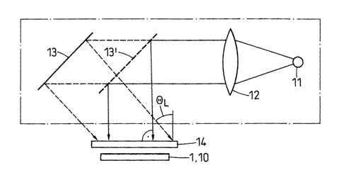
In a subsequent step, the photoresist layer 10 is exposed
for 70 s. For this purpose, the substrate 1 is. introduced
into the setup according to Fig. 5, which is a mask aligner
MA4~of Suss, Munich, comprising a modified mercury-vapour
lamp 11 having a modified end-stage optical system 12 and
folding mirror 13. The optical system 12 comprises a
bandpass filter which, for example, filters out the I-line
at a wavelength of 365 nm, and a polarizer, which preferably
produces s-polarised light. To improve the parallelism of
the beams, the fly's eye is removed from the beam path, a
lamp with as small an arc as possible is used and is
positioned as far away from the substrate as possible.
The exposure occurs through a phase mask 14. It comprises a
substrate of transparent material, in the example quartz,
with a large-area grating structure, a diffraction grating
bearing a layer of nontransparent material, in the example
chromium, which is interrupted - in the example, by regu-
larly spaced, consecutive strips. Phase masks of this type
are supplied by Ibsen in Farum (Denmark), and are manufac-
tured approximately as follows:
A quartz substrate 15 is covered with a photoresist layer 16
(Fig. 7a) and the latter is exposed to light using the laser
two-beam interference method, and developed (Fig. 7b). Then
tvoawn\l.,aa\YOe~nWO3%Al\AOOS'm~.art.doc
CA 02399651 2002-07-26
13
a full-area diffraction grating is produced on the surface
of the quartz substrate 15 by etching and subsequent removal
of the photoresist (Fig. 7c). Said surface is then
completely covered with a chromium layer 17 (Fig. 7d). A
continuous photoresist layer 18 is then applied to the
chromium layer 17 (Fig. 7e) and exposed through a mask
structured by electron beam or laser writing. The photo-
resist is then developed (Fig. 7f) and the chromium layer 17
is removed by etching from the parts not covered by photo-
resist. Finally, the residues of the photoresist layer 18
are removed to finish the phase mask 14 (Fig. 7g). The
structure of the mask thus determines which parts of the
phase mask are transparent.
The substrate 1 is arranged underneath the phase mask 14 in
such a way that the photoresist layer 10 is in vacuum
contact with said phase mask. The upper side of the phase
mask 14 is exposed at an angle which approximately corre-
sponds to the Lithrow angle OL, which is the angle at which
the angle of incidence is equal to the angle of first-order
diffraction, and in particular deviates by no more than 10°,
preferably by no more than 5°, from said angle. Under these
conditions, a pronounced diffraction pattern whose structure
corresponds to that of the grating of the phase mask 14
forms in the near field below the transparent regions of the
phase mask 14 (Fig. 6). Alternatively, the phase mask 14 can
also be exposed at an angle which approximately corresponds
to 0°, i.e., vertical incidence, or at an angle that does
not deviate from it by more than 10°, preferably not by more
than 5° (folding mirror 13' shown in dashed lines). In this
case, the diffraction pattern in the near field of the phase
mask 14 has half the grating period of that mask.
T:\Daf~n\H><N\Pat~nl\032BAL\A009',rtwn.002dx
CA 02399651 2002-07-26
14
After exposure the Aquatar layer is removed by washing with
deionized water, and the photoresist is then developed (Fig.
4b). Those parts of the surface of substrate 1 which are not
covered with photoresist are then etched with Ar and CHC1F2
at a pressure of 0.02 mbar in a parallel-plate reactor with
capacitive excitation of the plasma at 13.6 MHz and an RF
power of 50 W. The etch depth is 20 nm. The photoresist is
then removed. For this purpose, it is first subjected to
reactive ion etching for 60 s in an oxygen plasma at a pres-
sure of 0.2 mbar and an RF power of 50 W, then detached with
Remover AZ100, Deconex, and deionized water (Fig. 4d).
Finally the layer 2 is applied by reactive pulsed DC magne-
tron sputtering or by DC magnetron sputtering superimposed
with an AC frequency between 1 kHz and 1 MHz, in a Balzers
MSP1000 unit, similarly as described in EP-A-0 508 359
(Fig. 4e). This step is carried out in an Ar-02 atmosphere
at a pressure of 3.7 ,bar. The target material is tantalum.
Finally, the evanescent field sensor plate is cut to its
final size by wafer sawing.
Particularly on account of exposure through a phase mask
that can be reused practically as often as desired, the
process described permits the production of elements with
grating structures, particularly diffractive coupling
gratings, in large numbers and in a simple manner. The fact
that the phase mask is structured by the two-beam inter-
ference method also implies that large defect-free grating
structures having surface areas of 10 cma and more can be
produced on it with high precision, whereas other structur-
ing methods such as electron beam writing are not suitable
for this purpose owing to their virtually unavoidable
stitching errors. Therefore, large optical elements with
large-area gratings of high quality and uniformity can be
1:\Oalen\lad~\Paf~nt\OJ~AAI\AOOQ\wo_~.DOl.doc
CA 02399651 2002-07-26
produced, not only as final products but also as semi-
finished plates which by wafer sawing, scribing and breaking
or laser cutting can then be separated into smaller final
products which thus can be produced very economically and in
5 high quality.
Evanescent field sensor plates can of course also be pro-
duced in geometries and optical properties corresponding to
other standards or requirements. Thus, another evanescent
field sensor plate can have dimensions of 57 mm x 14 mm
10 x 0.7 mm and be provided with two strip-shaped'coupling
gratings having a width of 0.5 mm each which are symmetric-
ally arranged in parallel with the long sides, and have a
mutual distance of 9 mm. The grating period A = 318 nm, the
grating depth 12 nm, while otherwise the properties of the
15 layer and coupling gratings are the same as in the first
example. In this case the coupling angle O - -12.14° at a
wavelength of 633 nm, varying parallel to the lines by at
most 0.15°/cm. The deviation from a mean value remains below
0.5° everywhere on the evanescent field sensor plate. For
the production of a semifinished plate from which the indi-
vidual evanescent field sensor plates are then obtained by
water sawing, a phase mask is employed which measures
150 mm x 150 mm and has a region with a grating of grating
period 318 nm measuring 115 mm x 115 mm. The regions corre-
sponding to the coupling gratings are bare while the
remaining portion of the grating is again masked by a
nontransparent layer, particularly a chromium layer. Other-
wise the production proceeds as described above.
A further example is an evanescent field sensor plate meas-
uring 75 mm x 113.5 mm x 0.7 mm which as to its basic
features essentially corresponds to Fig. 1, and which bears
AMENDED
SHEET
T:\D~ot~n\T~#s\POtan~\03~EM\A009'msn.002.r1x
CA 02399651 2002-07-26
16
13 strip-shaped coupling gratings each 0.5 mm wide which are
parallel to the broadside and have distances between neigh-
boring strips of 8.5 mm each. Layer and grating properties
correspond to those of the second example. The coupling
angle O - -11.48° at a wavelength of 633 nm, varying
parallel to the lines by at most 0.05°/cm. Over the entire
evanescent field sensor plate it departs from a mean value
by at most 0.4°. The evanescent field sensor plate can be
expanded to a microtitre plate with 8 x 12 cavities by
adding a suitable top portion.
Apart from the embodiments of optical elements having grat-
ing structures produced by the process according to the
invention and used in chemical analysis, as portrayed above,
embodiments for applications in communications technology
are particularly pertinent. Such elements are suited above
all as highly efficient optical couplers such as those
employed in fibre-optic networks.
A first example of such a coupler is represented in Figs. 8a
and 8b. On a substrate 1 consisting of a glass plate 19 and
a layer 20 of transparent material, a coupling grating 3
formed as a line grating of constant grating period is
arranged. The layer 20 is covered by a transparent layer 2,
consisting for instance of Ta205. Layer 2 acts as a wave-
guide. The coupling grating 3 reflects light of a particular
wavelength ~,H according to the wavelength-dependent reflec-
tivity R schematically represented in Fig. 9a, while incid-
ent light of all other wavelengths is transmitted. This is
shown in Figs. 9b-d, where Fig. 9a shows the incident wave-
lengths, Fig. 9b the reflected wavelength ~.8, and Fig. 9c
the transmitted wavelengths. Using the coupler it is thus
possible to filter out a particular wavelength, for instance
T:\Dalw\T~M~\PW~nI\O;IIMI\AOOi\,.~.W2.COc
CA 02399651 2002-07-26
17
in a fibre-optic network using wavelength multiplexing.
Thanks to the high grating quality, the full width at half
maximum of the reflectivity R as a function of wavelength is
very small. Hence even with wavelengths very closely spaced,
it is possible to highly efficiently separate a wavelength.
An example for the use of such a coupler is shown in Fig.
10. Two parallel stripe waveguides 21a, b of known structure
are running parallel at a very small mutual distance in a
coupling region 22, in such a way that 50 % of the light
conducted in the first stripe waveguide 21a is. transferred
to the second stripe waveguide 21b, and vice versa. In the
final segment of the first stripe waveguide 21a, a coupler
23 with a coupling grating 3 according to Figs. 8a and b is
incorporated which selectively reflects light having a
wavelength ~,3.
When signals having wavelengths ~,1, ~.2, ~.3. ~.4 etc. are fed
into the first stripe waveguide 21a at an input 24, then on
one hand 50% of all signals in the coupling region 22 axe
transferred to the second stripe waveguide 21b where they
are conducted to a first output 25a, while the signals
remaining in the first stripe waveguide 21a are conducted to
a second output 25b, except for the signal of wavelength ~,3
corresponding to the ~,B according to Figs. 9a-d which is
reflected at the coupler 23 so that in the coupling region
22, 50% of its intensity transfer into the second stripe
waveguide 21b where the signal is conducted in a direction
opposite to that of the signals transferred directly from
the first stripe waveguide 21a, and reaches a third output
25c where finally it has been isolated and can be further
processed. The signals of outputs 25a and b can be
T:\Da1~n\T~KN\PGtMf\~28A~\AOO9'man.001.~ioc
CA 02399651 2002-07-26
18
recombined to a signal differing from the original one only
by a 50 % attenuation of the signal with wavelength ~,3.
The coupler 23 can be completely integrated into the first
stripe waveguide 21a, in such a way that this has the same
structure as coupler 23 and this coupler forms a single part
with the first stripe waveguide 21a. The only distinction of
coupler 23 is then its bearing the coupling grating 3.
A second example of a coupler is represented in Figs. lla
and b. In a longitudinal direction on top of a~rectangular
substrate 1 of glass, for instance Schott DESAG AF 45 with a
refractive index of 1.52, two coupling gratings, an input
coupling grating 3a and an output coupling grating 3b, are
arranged consecutively at a mutual distance, each extending
over the full width of the coupler. The input coupling
grating 3a has a grating period of A1 = 981 nm and a grating
depth of 6 nm, the output coupling grating 3b has a grating
period of A2 = 1350 nm and a grating depth of 12 nm. The
upper side of substrate 1 is covered by a continuous trans-
parent layer 2 consisting of Ta205 and having a refractive
index of 2.1. Its thickness is 400 nm.
The coupler can be used as a drop filter monitoring and
stabilising the intensity of a light beam, for instance a
line of a multimode laser. To this end (Fig. 12), the
coupler 23 described above is so arranged between the ends
of a first optical fibre 26a and a second optical fibre 26b
arranged in the continuation of the former that the input
coupling grating 3a faces the end of the latter while the
former faces the bottom side of coupler 23. The light
supplied by the first optical fibre 26a passes through the
part of the coupler 23 carrying the input coupling grating
3a while a fraction of the light of the 1550 nm line
T:\Dot~n\ThM\PaNnf\03't&AL\A009\_,msnA02.doc
CA 02399651 2002-07-26
19
corresponding to less than 0.01 of its intensity is coupled
into the layer 2 by said grating. At the output coupling
grating 3b, light is coupled out at an angle of 30° and
reaches an appropriately disposed photodetector 27 the
output signal of which is a measure of intensity of the
monitored line. Owing to the high precision of the input
coupling grating 3a, the input coupling is highly
wavelength-sensitive, the full width at half maximum of the
intensity distribution being a mere 0.01 nm, so that a
specific monitoring of a single wavelength is possible even
where the wavelengths are closely spaced, as desired in
wavelength multiplexing in the interest of a high trans-
mission capacity.
A third example of an optical coupler according to the
invention is represented in Figs. 13a and b. A rectangular
substrate 1 consists of a glass plate 19 with a refractive
index of 1.586 and a transparent layer 20 of Ti02 with a
refractive index of 2.4 covering the upper face of this
glass plate in a thickness of 285 nm. The upper face bears a
coupling grating 3 occupying its full width which has been
produced by removing layer 20 completely in a pattern of
lines, and is covered by a further transparent layer 2
consisting of MgFz which is 342 nm thick and has a refrac-
tive index of 1.38. The grating depth thus corresponds to
the thickness of layer 20, and is 285 nm. The grating period
A(x) varies linearly in a direction normal to the grating
lines, increasing from A1 = 970 nm to A2 = 97? nm.
When producing the coupler, layers 20 and 2 can be applied
as described in connection with the first example of an
evanescent field sensor plate. Production of the coupling
grating 3 after application of the layer 20 also occurs as
described there. In this operation, a phase mask is used
1:\DaHn\7wxb\Palenh~2lAL\AODqLmen.OD2.doe
CA 02399651 2002-07-26
whose grating varies appropriately, hence linearly in the
present case. Such phase masks can be produced by appropri-
ately bending a flexible master copy and applying a grating
structure using the two-beam interference method. The phase
5 mask is derived by replication, that is, by making an
impression of the reflattened master copy.
The coupler can advantageously be used in a device for moni-
toring and stabilising the wavelength of a laser 28 (Fig.
14) the light of which is fed into a light-conducting fibre
10 29, for instance a glass fibre, of a fibre network. The
device comprises a semi-transmissive mirror 30 arranged in
the path of the light beam coming from the laser 28, follow-
ed by a first optical system 31 to expand, and a second
optical system 32 to collimate the part of the light beam
15 deflected by the mirror 30. Following after the optical
systems, the coupler 23 described above is arranged in the
light beam normal to the beam direction, in such a way that
the beam strikes the coupling grating 3. Mounted directly
beneath the coupler 23 is a detector system with two photo-
20 detectors 33a and b which are arranged so as to be immedia-
tely adjacent one behind the other and normal to the lines
in such a way that the part of the light beam transmitted by
a first portion of the coupling grating 3 where the grating
period is between Al and an intermediate value Ai strikes
the first photodetector 33a while the part transmitted by
the remaining portion of the coupling grating 3 where the
grating period is between Ai and AZ strikes the second
photodetector 33b. The photodetectors 33a and b can be
displaced so that A;, is adj ustable .
The transmissivity of the coupler 23 is a sensitive function
of wavelength and of the grating period A. Because of the
r:voaW n\T.atvrateM~0326AtAOW'ma,.ao~.doe
CA 02399651 2002-07-26
21
position-dependent variation of the grating period A(x),
therefore, it exhibits a specific wavelength dependence for
the incident light which depends on its position. This is
shown in Fig. 15, where the transmissivity T can be gathered
as a function of position on the coupling grating 3 for
three very close wavelengths (1549.5 nm, 1550 nm,
1550.5 nm). The minimum of the transmissivity curve shifts
to larger or smaller grating periods as the wavelengths
increase or decrease, and hence to a different position on
the grating. This in turn gives rise to changes in the
relative intensities of the light captured by the photo-
detectors 33a and 33b, which has a direct effect on the size
of their output signals Ia, Ib.
For the purposes of stabilising a particular wavelength, one
can then roughly adjust the position of the detector
arrangement in accordance with the wavelength of interest,
and then calculate a value
Q = (Ia-Ib) ~ (Ia+Ib)
and reduce it to zero by shifting the detector arrangement.
Any change in wavelength of the light beam coming from the
laser 28 will give rise to a positive or negative deviation
of the value of Q from zero, depending on the direction of
the wavelength change, and can be compensated by correspond-
ing control of the laser 28. The intensity of the light beam
is unimportant here. Only the intensity distribution of the
expanded light beam which may not be homogeneous but follow
a gaussian distribution, for instance, might eventually
cause perturbations, but this can then be compensated by
appropriate arrangement or extension of the optical systems
or by calculation.
T:\DoHn\Ta~M\PafeM\0328A1\A009\.~~~.002.doe
CA 02399651 2002-07-26
22
The optical elements according to the invention can be modi-
fied in many respects without departing from the basic
concept of the invention. Thus, in many cases deviations
from the mean value of up to 0.3° or even up to 0.5° over
the entire element or even over a coupling grating can be
admitted. For the evanescent field sensor plates, too, it
will often be sufficient when the changes in coupling angle
O along the grating lines are not larger than 0.1°/cm.
Many deviations or special adaptations to particular
requirements are possible as well in the production process.
Thus, even in the exposure step which is decisive for the
process, the photoresist layer may by spaced apart from the
phase mask, which facilitates the process. However, it must
be arranged in the near field, that is, at a distance which
as a rule is smaller than 100 Vim, for the diffraction
pattern to be sufficiently pronounced. This distance may
perhaps be between 2 ~m and 100 ~.m. Instead of a mercury-
vapour lamp, a laser can also be used as the light source,
particularly an excimer laser or an argon laser. Apart from
Ta205, other substances can be used as materials for the
layer, particularly Nb205, Ti02, Zr02, A1203, SiOz-Tit~2, Hf02,
Y2O3, SiOXNy, Si3N4, HfOXNY, AlOXNy, TiOXNy, MgF2 oder CaF2.
Ion-enhanced evaporation or plasma-enhanced gas phase
deposition can be used as coating methods. Finally, several
layers differing in their composition and thickness can be
applied consecutively, as described in one of the embodi-
ments portrayed.
Phase masks need not be produced directly by the two-beam
interference method but can be copied directly or indirectly
from a master copy thus produced. They can be used several
times with layers interrupted in diverse manner when diverse
arrangements of coupling gratings and the like are to be
AMENL'~ED
S H~EET
T:\Dat~n\TaKH\Patenf\0328AL\A009'men.002.doc
CA 02399651 2002-07-26
23
generated while maintaining a constant grating period.
Instead of a nontransparent layer, a suitable layer of
transparent material can also be used. Thus, the grooves of
the grating can be filled by a material having the refract-
s ive index of the phase mask substrate.
The phase mask can be antireflection-coated. In this case it
may not be necessary to apply a reflection-reducing layer to
the photoresist layer, which facilitates the production of
series of grating structures on the substrates. For anti-
reflection, a layer having a refractive index between that
of the phase mask substrate and that of air, and for in-
stance consisting of MgF2, is applied to the side of the
phase mask facing the photoresist layer. At the same time
the grating must be adjusted in such a way that the inter-
fering diffraction orders of the transmitted light will
again have the same intensity. This adjustment can occur by
changing the groove-to-land ratio and the grating depth,
which are readily calculated with the aid of programmes
known among experts.
List of reference symbols
1 Substrate
2 Transparent layer
3 Coupling grating
4 Added top part
5 Cover plate
6 Opening
7 Tube section
8 Cavity
9 Optical system
10 Photoresist layer
11 Mercury-vapour lamp
T:\Datan\Texfe\PafanT\0~2EAL\A009\..~.002.doe
CA 02399651 2002-07-26
24
12 Optical system
13, 13' Folding mirror
14 Phase mask
15 Quartz substrate
16 Photoresist layer
17 Chromium layer
18 Photoresist layer
19 Glass plate
20 Layer
2la,b Stripe waveguides
22 Coupling region
23 Coupler
24 Input
25a,b,c Outputs
26a,b Optical fibres
27 Photodetector
28 Laser
29 Optical fibre
30 Semi-transmissive mirror
31 First optical system
32 Second optical system
33a,b Photodetectors