Note: Descriptions are shown in the official language in which they were submitted.
CA 02399673 2002-08-23
1
TITLE OF THE INVENTION:
Thermophotovoltaic Device
FIELD OF THE INVENTION
The present invention relates to a thermophotovoltaic
device.
BACKGROUND OF THE INVENTION
7_0 U.S. Patent 5,403,405 (Fraas et al 1995), U.S. Patent
5, 551, 992 (Fraas 1996) , U. S. Patent 5, 753, 050 (Charache et al
1998) are examples of thermophotovoltaic devices.
A problem experienced with thermophotovoltaic devices is
J_5 that only a fraction of the energy generated can be used by
the photovoltaic cells. Long wavelength energy can not be
used by the photovoltaic cells and can increase cell
temperature.
20 SUL~ARY OF THE INVENTION
What is required is a thermophotovoltaic device which is
less susceptible to the detrimental effects of long
wavelength energy.
25 According to the present invention there is provided a
thermophotovoltaic device which includes an energy source
compatible with thermophotovoltaic cells and
thermophotovoltaic cells. A dielectric filter, adapted to
filter mid-wavelength energy, is positioned between the
30 energy source and the thermophotovoltaic cells. A quartz
glass tube filter, adapted to recycle long wavelength energy,
is positioned between the energy source and the
thermophotovoltaic cells. The glass tube filter has dual
glass tubes with a space therebetween. The space is
35 evacuated to break the convection heat transfer path from the
energy source to the thermophotovoltaic cells.
CA 02399673 2002-08-23
2
The thermophotovoltaic device, as described above,
includes a simple and inexpensive infrared filter and thermal
insulator to drammatically improve efficiency by reducing
energy losses.
BRIEF DESCRIPTION OF T8E DRAWINGS
These and other. features of the invention will become
more apparent from the following description in which
reference is made to the appended drawings, the drawings are
7_0 for the purpose of illustration only and are not intended to
in any way limit the scope of the invention to the particular
embodiment or embodiments shown, wherein:
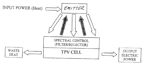
FIGURE 1 is a simplified block diagram of a
thermophotovoltaic system.
7_5 FIGURE 2 is a side elevation view of components for a
thermophotovoltaic device constructed in accordance with the
teachings of the present invention.
FIGURE 3 is a side elevation view, in section, of a
thermophotovoltaic device constructed in accordance with the
20 teachings of the present invention.
DETAILED DESCRIPTION OF T8E PREFERRED EM80DIM~NT
The preferred embodiment, a thermophotovoltaic device
will now be described with reference to FIGURES 1 through 3.
CA 02399673 2002-08-23
DESCRIPTION OF THE INVEf~'TION
Background
3
TPV systems consist of a heat source above about 1300 K, coupled with a
broadband or selective
emitter, thermophotovoltaic convener cells with or without a filter/reflector,
and a cooling and heat
recuperation system. Some attractions of this technology are:
~ High power densities -1-2 W/cmz are reported in prototype systems. Mature
systems
expected to be on the order of S W/cm''.
~ Quiet Operation -TPV conversion uses no moving parts (except cooling or
combustion air
fans in some designs) and can be expected to be essentially silent. This
feature makes it
attractive for military applications and recreational use.
~ Low Maintenance-due to lack of moving parts maintenance requirements will be
minimal.
~ Cogeneration - for high efficiency, TPV systems must include a heat recovery
system as a
part of cell cooling and to preheat fuel and air before combustion. TPV
devices are an
excellent candidate for combined heat and power applications.
~ Versatility-TPV systems may be fuelled by almost any combustible material,
although the
burner must be designed for that particular fuel in order to maintain high
efficiency.
~ Low emissions-are possible with well-designed burner/fuel selection.
A simplified TPV system schematic is shown in Figure 1.
Typical TPV units can include some or all of the following subsystems:
I. Heat source - a burner for efficient combustion of the fuel, be it liquid
or gaseous, hydrocarbon,
or even biomass. The burner design for TPV is not trivial due to relatively
low firing rates, high
operating temperatures, small size, uniform temperature distribution and high
efficiency
requirements. The burner may al:~o have means of recirculating exhaust gases
in order to preheat fuel
and combustion air to increase combustion efficiency.
2 Emitter-an IR radiation source (heated by the combustion) operating in the
temperature range of
1300 K to I 800 K. Temperatures below this can lead to low power densities and
low electrical
output, while operation above the maximum is not practical due to cost of high
temperature materials
and problems with ce(I cooling. The emitter material must have mechanical
stren~h at the operating
temperature, high emissivity and tolerance for thermal cycling. There are
generally two types of
radiators used:
~ Broadband emitters - basically a black body, behaving according to Planck
radiation law, where
radiation extends across a wide wavelength range. Only a fraction of energy
(dependent on
temperature) is radiated below 2.S Elm (equivalent to energy bandgap of O.S
eV) and can be used
effectively by photovoltaic cell. 'The remaining long wave energy (photons) is
not used by the
cells and can increase cell temperature. Ideally this energy is recycled back
to the radiator or used
to preheat the inlet filel and air. The most commonly used broadband emitter
material is silicon
carbide (SIC). SIC 1S aI1 exCellellt Infrared erTlltler rllatCl'lal w1111
hlgll en11SS1VlIy, g00d thCI11181
conductivity and relatively hood thermal shock resistance. At a temperature of
1800 K silicon
CA 02399673 2002-08-23
4
carbide has a radiation emission peak between 1.4 and 1.6 um.
~ Selective emitters - certain rare earth oxides (ytterbium, erbium, holmium)
radiate in a fairly
narrow band of wavelengths. The major disadvantages of these emitters are low
power density
due to very narrow emission bandwidths and low average peak emittance. A
solution to these
problems would be to increase emitter temperature, but this leads to shorter
material life and
lower fuel to radiant power conversion efficiency. There is also significant
radiation of
wavelengths longer than 3 pm and an IR filter should be used to reflect these
low energy level
photons back to the emitter. Variations of selective emitter design include:
~ matched emitters consisting of ceramic matrix composites with a refractory
oxide (such as
alumina, magnesia oxide or spine() doped with a d-series transition element.
Relatively broad
IR emission spectrum in the range 1.0 to 1.7 arm has been reported. This is
easier to match
with usable bandwidth of GaSb TPV cells. Another type of selective emitter
uses a
microstructured tungsten .surface with low emittance in the region above 2 pm.
Tungsten is
very stable at high temperatures in a vacuum, but oxidizes in air so it is
necessary to operate
this type of emitter in vacuum or in inert gas atmospheres.
~ multiband emitters built as a combination of two rare oxides, such as
Er~03/HoZO; and
Er~03/Yb~03 resulting in multiple peak spectrum radiation. One of the
manufacturing
methods for these emitters is a thermal plasma spray of a thin film onto
various substrates
(SiC or suitable ceramic oxide with reflective metal backing or reflective
metal layer
deposited on front of oxide substrate).
3. IR filter-for optimum system efficiency, the incident radiation should
match the recombination
spectrum of the photocell material. Excess energy should be reflected back to
the emitter and
preferably reabsorbed. To achieve this, single or multiple filters are placed
between the emitter and
the TPV cells. They may be inte~;rated with the TPV cell assembly. There are a
number of different
filter designs:
~ Interference or mesh filters similar to those used for microwave
frequencies. Generally the
dimensions of the array elements are a fraction of a wavelength, requiring
resolution less than 0.2
p.m. The state of the an conventional lithography is now about 0.1 um feature
size. This allows
mass manufacturing of the filter at costs probably lower than a dielectric
stack. The mesh filters
use Au as a base metal deposited on a dielectric substrate and as such have
good IR reflectivity
(>95%) at wavelengths longer than 2 pm.
~ Multilayer dielectric filters are based on interference effects, using
multiple layers of dielectric
films with varying refraction coefficients and different thieknesses.
Dielectric films have minimal
losses and it is possible to manufacture a filter with specific performance by
increasing the
number of layers.
4. TPV cells are narrow bandgap (0.5 to 0.7 eV) III-V semiconductor diodes
that convert photons
radiated from a thermal radiation source (at temperatures below 2000K) into
electricity. Photons
with energy greater than the semiconductor bandgap excite electrons from the
valence band to the
conduction band. The created electron-hole pairs are then collected by metal
electrodes and can
be utilized to power external loac s.
Basis of Invention
The basis of the invention described here is an improved filter system to
recycle z large fraction of the
longer wavelength energy to the emitter while reducing the convective heat
transter from the emitter
CA 02399673 2002-08-23
to the TPV cells. The concept is to combine dielectric filters (as described
above) that are positioned
directly on or in front of the TPV cell arrays with a dual quartz glass tube
filter with the space
between the quartz tubes evacuated to break the convection path. The
dielectric filters provide
recycling of mid-wavelength energy (up to about 3.5 micron wavelength) while
the quartz glass
recycles the longer wavelengths and the addition of the vacuum layer breaks
the convection heat
transfer path from the emitter to the cell arrays. This arrangement should
provide a simple and
inexpensive method of improving TPV system efficiency by reducing energy
losses.
A sketch of the basic components of the TPV system as conceived is given in
Figure 2. Figure 3
shows a cut-away view of the assembled system.
Estimated Efficiency of Spectral Control System
Use WS radiant tube burner with double wall GE 214 low OH fused silica thermos
to reduce long
wavelength IR by one third via 1/(n+1 ) heat shield formula (with n=2 and
assuming near planar
geometry). Also use dielectric filters from JXC for rnid wavelength band
spectral control.
Given an energy rate transfer budl;et of 7 W/cm2, we make the following
efficiency calculation.
Assume emitter temperature of 1 100 C or 1373 K.
Total Black Body power = 20. I 5 W/cm2.
power from Black Body for wavelength < 1.8 microns = 15%.
power from Black Body between 1.8 and 3.6 microns = 48%
power from BB for wavelengths longer than 3.6 microns = 37%
Power to receiver from various bands:
Less than 1.8 microns = 15% x 20.15 = 3.02 W/cm2
Between 1.8 to 3.6 microns = 10% x 48% x 20. I 5 = 0.97 W/cm2
(assumes 90% dielectric filter recycling)
Greater than 3.6 microns = 33% x 37% x 20.15 = 2.46 W/cm2
Total net power transferred from emitter = 6.45 W/cm2
Spectral efficiency = 3.02/6.45 = 47%
System electrical efficiency = 75% x 30% x 47% = 10.6%
Where 75% is chemical to radiation efficiency
And 30% is PV cell conversion efficiency.
Assume 80 mm diameter emitter and 250 mm long cell array,
Then emitter area will be 3.14 x 8 x 25 = 628 cm2.
Given 1 W(electric) /cm2, potential electrical output could be 600 W.This
corresponds to a 6
kW(thermal) burner which is in the operating range of the WS C80/800 burner.
CA 02399673 2002-08-23
6
The benefit of the evacuated quartz tube (in addition to long wave recycling)
is that it will reduce
convective heat transfer from the emitter to the cell arrays as demonstrated
in the calculations below.
T(0) T(I) T(2)
E(1) _ ~ E(1)
___
E(2) ~ - E(2)
---
E(0)
-~1
Calculate quartz shield temperatures given emitter at 1 100 C
Note that E(0) + E(2) = 2 E( 1 ) and E( I ) = 2 E(2)
from the energy balance at each quartz shield.
Therefore E(0) = 4 E(2) - E(2) = 3 E(2)
Assuming T(0) = 1100 C
Then E(0) = 37% x 20 W/cm2 = 7.4 W/cm2
And E(2) _ ( 1 /3) x 7.4 = 2.47 Wicm2
Also [T(2)/T(0)]4 = 2.47/20 = 0.124
Therefore T(2) = 0.593 x 1373 = 814 K = 541 C
And similarly T( I ) = 0.71 T(0) = 969 K = 696 C
Thus, instead of convective/conductive transfer in the air layer between the ~
I 100 C emitter and the
-30 C cells the quartz tube will transfer heat from the second quartz glass at
541 C to the ~30 C
TPV cells. This could reduce the heat loss through the cells by about 50%