Note: Descriptions are shown in the official language in which they were submitted.
CA 02399960 2002-07-31
WO 01/57961 PCT/USO1/02959
CONNECTOR WITH SHIELDING
BACKGROUND OF THE INVENTION
Electrical connectors are used in many electronic
systems. It is generally easier and more cost effective to
manufacture a system on several printed circuit boards that
are then joined together with electrical connectors. A
traditional arrangement for joining several printed circuit
boards is to have one printed circuit board serve as a
backplane. Other printed circuit boards, called daughter
boards, are connected through the backplane.
A traditional backplane is a printed circuit board with
many connectors. Conducting traces in the printed circuit
board connect to signal pins in the connectors so signals
may be routed between the connectors. Daughter boards also
contain connectors that are plugged into the connectors on
the backplane. In this way, signals are routed among the
daughter boards through the backplane. The daughter cards
often plug. into the backplane at a right angle. The
connectors used for these applications contain a right angle
bend and are often called "right angle connectors."
Connectors are also used in other configurations for
interconnecting printed circuit boards, and even for
connecting cables to printed circuit boards. Sometimes, one
or more small printed circuit boards are connected to
another larger printed circuit board. The larger printed
CA 02399960 2002-07-31
WO 01/57961 PCT/USO1/02959
circuit board is called a "mother board" and the printed
circuit boards plugged into it are called daughter boards.
Also, boards of the same size are sometimes aligned in
parallel. Connectors used in these applications are
sometimes called "stacking connectors" or "mezzanine
connectors."
Regardless of the exact application, electrical
connector designs have generally needed to mirror trends in
the electronics industry. Electronic systems generally have
gotten smaller and faster. They also handle much more data
than systems built just a few years ago. These trends mean
that electrical connectors must carry more and faster data
signals in a smaller space without degrading the signal.
-
Connectors can be made to carry more signals in less
space by placing the signal contacts in the connector closer
together. Such connectors are called "high density
connectors." The difficulty with placing signal contacts
closer together is that there is electromagnetic coupling
between the signal contacts. As the signal contacts are
placed closer together, the electromagnetic coupling
increases. Electromagnetic coupling also increases as. the
speed of the signals increase.
In a conductor, electromagnetic coupling is indicated
by measuring the "cross talk" of the connector. Cross talk
is generally measured by placing a signal on one or more
signal contacts and measuring the amount of signal coupled
to the contact from other neighboring signal contacts. In a
traditional pin in box connector mating in which a grid of
pin in box matings are provided, the cross talk is generally
recognized as a sum total of signal coupling contributions
from each of the four sides of the pin in box mating as well
as those located diagonally from the mating.
- 2 -
CA 02399960 2002-07-31
WO 01/57961 PCT/USO1/02959
A traditional method of reducing cross talk is to
ground signal pins within the field of the signal pins. The
disadvantage of this approach is that it reduces the
effective signal density of the connector.
To make both a high speed and high density connector,
connector designers have inserted shield members in
proximity to signal contacts. The shields reduce the
electromagnetic coupling between signal contacts, thus
countering the effect of closer spacing or higher frequency
signals. Shielding, if appropriately configured, cari also
control the impedance of the signal paths through the
connector, which can also improve the integrity of signals
carried by the connector.
An early use of shielding is shown in Japanese patent
disclosure 49-6543 by Fujitsu, Ltd. dated February 15, 1974.
US patents 4,632,476 and 4,806,107, both assigned to AT&T
Bell Laboratories, show connector designs in which shields
are used between columns of signal contacts. These patents
describe connectors in which the shields run parallel to the
signal contacts through both the daughter board and the
backplane connectors. Cantilevered beams are used to. make
electrical contact between the shield and the backplane
connectors. Patents 5,433,617; 5,429,521; 5,426,520 and
5,433,618, all assigned to Framatome Connectors
International, show a similar arrangement. The electrical
connection-between the backplane and shield is, however,
made with a spring type contact.
Other connectors have the shield plate within only the
daughter card connector. Examples of such connector designs
can be found in patents 4,846,727, 4,975,084, 5,496,183 and
5,066,236, all assigned to AMP, Inc. Another connector with
shields only within the daughter board connector is shown in
US patent 5,484,310, assigned to Teradyne, Inc.
- 3 -
CA 02399960 2002-07-31
WO 01/57961 PCT/USO1/02959
A modular approach to connector systems was introduced
by Teradyne Connection Systems, of Nashua, New Hampshire.
In a connector system called HD+~, multiple modules or
columns of signal contacts are arranged on a metal
stiffener. Typically, 15 to 20 such columns are provided in
each module. A more flexible configuration results from the
modularity of the connector such that connectors
"customized" for a particular application do not require
specialized tooling or machinery to create. In addition,
many tolerance issues that occur in larger non-modular
connectors may be avoided.
A more recent development in such modular connectors
was introduced by Teradyne, Inc. and is shown in US patents
5,980,321 and 5,993,259 which are hereby incorporated by
reference. Teradyne, Inc., assignee of the above-identified
patents, sells a commercial embodiment under the trade name
VHDMs'" .
The patents show a two piece connector. A daughter
card portion of the connector includes a plurality of
modules held on a metal stiffener. Here, each module~is
assembled from two wafers, a ground wafer and a signal
wafer. The backplane connector, or pin header, includes
columns of signal pins with a plurality of backplane shields
located between adjacent columns of signal pins.
Yet another variation of a modular connector is
disclosed in patent application 09/199,126 which is hereby
incorporated by reference. Teradyne Inc., assignee of the
patent application, sells a commercial embodiment of the
connector under the trade name VHDM - HSD. The application
shows a connector similar to the VHDM'i'M connector, a modular
connector held together on a metal stiffener, each module
being assembled from two wafers. The wafers shown in the
- 4 -
CA 02399960 2002-07-31
WO 01/57961 PCT/USO1/02959
patent application, however, have signal contacts arranged
in pairs. These contact pairs are configured to provide a
differential signal. Signal contacts that comprise a pair
are spaced closer to each other than either contact is to an
adjacent signal contact that is a member of a different
signal pair.
- S -
CA 02399960 2002-07-31
WO 01!57961 PCT/USO1/02959
SUMMARY OF THE INVENTION
As discussed in the background, high density and high
speed connectors
As discussed in the background, higher speed and higher
density connectors are required to keep pace with the
current trends in the electronic systems industry. With
these higher densities and higher speeds however
electromagnetic coupling or cross talk between the signal
contacts becomes more problematic.
An electrical connector having mating pieces with
shields in one piece oriented transversely to the shields in
a second piece is therefore provided. In a preferred
embodiment, one piece of the connector is assembled from
wafers with shields positioned between the wafers. The
shields in one piece have contact portions associated
therewith for making electrical connection to shield in the
other piece. With such an arrangement, a connector is
provided that is easily manufactured and possesses improved
shielding characteristics.
In other embodiments, the second piece of the connector
is manufactured from a metal and includes slots into which
signal contacts surrounded.by an insulative material are
inserted. With such an arrangement, the signal contacts are
provided an additional four-walled shield against cross
talk.
- 6 -
CA 02399960 2002-07-31
WO 01/57961 PCT/USO1/02959
BRIEF DESCRIPTION OF THE DRAWINGS
The foregoing and other objects, features and
advantages of the invention will be apparent from the
following more particular description of a Connector with
Egg-Crate Shielding, as illustrated in the accompanying
drawings in which like reference characters refer to the
same parts throughout the different views. For clarity and
ease of description, the drawings are not necessarily to
scale, emphasis instead being placed upon illustrating the
principles:of the invention.
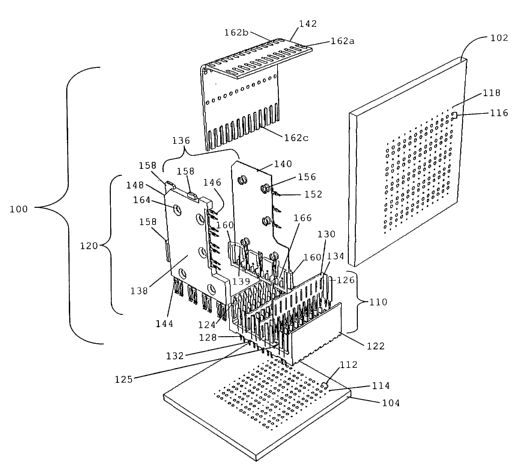
FIG. 1 is an exploded view of a connector assembly made
according to one embodiment of the invention.
FIG. 2 is the backplane connector of FIG. 1.
FIG. 3 is the backplane shield plate 130 of FIG. 1.
FIG. 4 is an alternate view of a representative signal
wafer of FIG. 1.
FIG. 5 is a view of the daughter card shield plate 140
of FIG. 1 prior to molding.
FIG. 6 is a top sectional view of a shielding pattern
that results when the two pieces of the connector
of FIG. 1 are mated.
FIG. 7 is an alternate embodiment of the connector 100
of FIG. 1.
FIG. 8 is an alternate embodiment of the wafer of FIG.
4.
FIG. 9 is an alternate embodiment of the backplane
connector of FIG. 2.
FIG. 10 is an alternate embodiment of the backplane
shield plate of FIG. 3.
FIG. 11 is an alternate embodiment of the daughter card
shield plate of FIG. 5.
CA 02399960 2002-07-31
WO 01/57961 PCT/USO1/02959
DESCRIPTION OF THE PREFERRED EMBODIMENT
FIG. 1 is an exploded view of a connector assembly 100
made in accordance with one embodiment of the invention.
The connector assembly 100 includes two pieces. The first
piece is connected to a daughter card 102 and may be
referred to as a daughter card connector 120. The second
piece is connected to a backplane 104 and may be referred to
as a backplane connector 110. The daughter card connector
120 and backplane connector 110 are intermatable and
together form a substrate-to-substrate connector. Here, the
connector is shown and will be described as connecting a
backplane and daughter card. However, the techniques
described herein may also be implemented in other substrate
to substrate connectors and also in cable to substrate
connectors.
Generally, multiple backplane connectors are connected
to a backplane and are aligned side by side.
Correspondingly, multiple daughter card connectors are
provided on a daughter card to mate with the multiple
backplane connectors. Hers, for purposes of illustration and
ease of description, only a single backplane connector 110
and daughter card connector 120 are shown.
Referring also to FIG. 2, the support for the backplane
connector 110 is a shroud 122 that is preferably formed by
an injection molding process using an insulative material.
Suitable insulative materials are a plastic such as a liquid
crystal polymer (LCP), a polyphenyline sulfide (PPS), or a
high temperature nylon. The shroud 122 includes sidewall
grooves 124 in opposing sides of the shroud 122. As will be
discussed below, these sidewall grooves 124 are used to
align elements of the daughter card connector 120 when the
two connectors 110, 120 are mated. Running along a floor of
the shroud 122, perpendicular to the sidewall grooves are a
_ g _
CA 02399960 2002-07-31
WO 01/57961 PCT/USO1/02959
plurality of narrow grooves or trenches 125 which receive a
backplane shield 130.
The backplane connector 110 includes an array of signal
conductors that transfer signals between the backplane 104
and the daughter card 102 when the backplane connector 110
is mated with the daughter card connector 120. Disposed at
a first end of the signal conductors are mating contacts
126. In a preferred embodiment, the mating contacts 126
take the form of signal blades 126 and are configured to
provide a path to transfer a differential signal. A'
differential signal is provided by a pair of conduction
paths 126a, 126b which is typically referred to as a
differential pair. The voltage difference between the two
paths represents-the differential signal pair. In a
preferred embodiment, there are eight rows of signal blades
126 in each column. These eight signal blades may be
configured to provide eight single ended signals or as
mentioned above, four differential signal pairs.
The signal blades 126 extend through the shroud 122 and
terminate in tail elements 128, which in the preferred
embodiment, are adapted for being press fit into signal
holes 112 in the backplane 104. Signal holes 112 are plated
through holes that connect to signal traces in the backplane
104. FIG. 1 shows the tail elements as "eye of the needle"
tails however, the tail elements 128 may take various forms,
such as surface mount elements, spring contacts, solderable
pins, etc.
Referring also to FIG. 3, a plurality of shield plates
130 is provided between the columns of signal blades 126,
each disposed within one of the plurality of trenches 125.
The shield plates 126 may be formed from a copper alloy such
as beryllium copper or, more typically, a brass or phosphor
bronze. The shield plates 130 are also formed in an
_ g _
CA 02399960 2002-07-31
WO 01/57961 PCT/USO1/02959
appropriate thickness in the range of 8 - 12 mils to provide
additional stability to the structure.
In a single-ended embodiment, the shield plates are
disposed between the columns of signal blades 126. In the
preferred embodiment, the shield plates 130 are disposed
between pairs of signal blades 126. The shield plates 130
are substantially planar in form and terminate at a base end
in tail elements 132 adapted for being press fit into ground
holes 114 in the backplane 104. In the preferred
embodiment, the tail elements 132 take the form of "eye of
the needle" contacts. Ground holes 114 are plated through
holes that connect to ground planes on the backplane 104.
In a preferred embodiment, the shield plate 130 includes ten
tail elements 132. A beveled edge (not labeled) is provided
at the top end of the shield plate 130. In one embodiment,
the shield plates 130 include strengthening ribs 134 on a
first face of the shield plate 130.
Referring again to FIG. 1, the daughter card connector
120 is a modular connector. That is, it includes a
plurality of modules or wafers 136. The plurality of wafers
are supported by a metal stiffener 142. Here, a '
representative section of the metal stiffener 142 is shown.
Also shown, is an exemplary wafer 136. In a preferred
embodiment, the daughter card connector 120 includes a
plurality of wafers stacked side-by-side, each wafer being
supported by the metal stiffener 142.
The metal stiffener 142 is generally formed from a
metal strip, typically a stainless steel or an extruded
aluminum, and is stamped with a plurality of apertures 162.
The plurality of apertures 162 are adapted to accept
features 158 from each of the plurality of wafers 136 that
combine to retain the wafers 136 in position. Here, the
metal stiffener 142 includes three apertures 162 to retain
- 10 -
CA 02399960 2002-07-31
WO 01/57961 PCT/USO1/02959
the wafer's position; a first 162a located at a first end,
the second 162b located within a substantially ninety degree
bend in the metal stiffener and the third 162c located at a
second end of the metal stiffener 142. When attached, the
metal stiffener 142 engages each of two edges on the wafers
136.
Each wafer 136 includes a signal portion 148 and a
shielding portion 140. Both the signal portion 148 and
shielding portion 140 include an insulative housing 138, 139
which is insert molded from an insulative material. ,Typical
materials used to form the housings 138, 139 include a
liquid crystal polymer (LCP), a polyphenyline sulfide (PPS)
or other suitable high temperature resistant insulative
material.
Disposed within the insulative housing 138 of the
signal portion 148 are conductive elements that extend
outward from the insulative housing 138 through each of two
ends. The conductive elements are formed from a copper
alloy such as beryllium copper and are stamped from a roll
of material approximately eight mils thick.
At a first end, each conductive element terminates in a
tail element 146 adapted to be press fit into a signal hole
116 in the daughter card 102. Signal holes 116 are plated
through holes that connect to signal traces in the daughter
card 102. At a second end, each conductive element
terminates in a mating contact 144. In a preferred
embodiment, the mating contact takes the form of a beam
structure 144 adapted to receive the signal blades 126 from
the backplane connector 110. For each signal blade 126
included in the backplane connector 110, there is provided a
corresponding beam structure 144 in the daughter card
connector 120.
- 11 -
CA 02399960 2002-07-31
WO 01/57961 PCT/USO1/02959
In a preferred embodiment, eight rows, or four
differential pairs, of beam structures are provided in each
wafer 136. The spacing between differential pairs as
measured across the wafer is 1.6mm to 1.8mm. The group to
group spacing, also measured across the wafer, is
approximately 5mm. That is, the spacing between repeating,
identical features such as between the left signal blade 126
in a first pair and the left signal blade 126 in an adjacent
pair is 5mm.
Included on a third and fourth end of the insulative
housing 138 are multiple features 158a - 158c that are
inserted into the stiffener apertures 162 to fasten the
wafer 136 to the stiffener 142. The features 158a, 158b on
the fourth end take the form of tabs formed in the
insulative housing while the feature 158c on the third end
is a hub which is adapted to provide an interference fit in
the third aperture 162c in the metal stiffener 142.
The shielding portion of the wafer 136, also referred
to as the shield 140, is formed of a copper alloy, typically
a beryllium copper, and is stamped from a roll of material
approximately eight mils thick. As described above, the
shield is also partially disposed in insulative material.
The insulative material on the shield 140 defines a
plurality of cavities 166 in which the signal beams 144
reside. Adjacent to these defined cavities 166 on the first
and third ends of the wafer 136 are shroud guides 160a, 160b
which engage the sidewall grooves 124 of the backplane
connector 110 when the daughter card 120 and backplane 110
connectors are mated, thus aiding the alignment process.
The combination of the sidewall grooves 124 and the shroud
guides 160a, 160b prevent unwanted rotation of the wafers
136 and support uniform spacing between the wafers 136 when
the backplane connector 110 and the daughter card connector
- 12 -
CA 02399960 2002-07-31
WO 01/57961 PCT/USO1/02959
120 are mated. The wafer pitch, or spacing between the
wafers is within the range of 1.75mm to 2mm, with a
preferred wafer pitch being 1.85mm.
The sidewall grooves 124 also provide additional
stability to the wafers by balancing the forces of the
mating contacts. In the preferred embodiment, the signal
blades 126 of the backplane connector 110 mate with the
signal beams 144 of the daughter card connector 120. The
nature of this mating interface is that the forces from the
beams are all applied to a single side, or surface of the
blades. As a result, the forces provided by this mating
interface are all in a single direction with no opposing
force available equalize the pressure. The sidewall grooves
124 provided in-the backplane shroud 122 equalize this force
thus providing stability to the connector 100.
Disposed at a first end of the shield 140 are a
plurality of tail elements. Each tail element is adapted to
be press fit into a ground hole 118 in the daughter card
102. Ground holes 118 are plated through holes that connect
to ground traces in the daughter card 102. In the
illustrated embodiment, the shield 140 includes three tail
elements 152 however, in a preferred embodiment four tail
elements 152 are included. In a preferred embodiment, the
tail elements take the form of ~~eye of the needle" elements.
At a second end of the shield 140 are mating contacts
150. In the illustrated embodiment, the mating contacts 150
take the form of beams that are adapted to receive the
beveled edge of the backplane connector shield 130. The
resulting connection between the shields 130, 140 provides a
ground path between the daughter card 102 and the backplane
104 through the connectors 110, 120.
- 13 -
CA 02399960 2002-07-31
WO 01/57961 PCT/USO1/02959
Referring now to FIG. 4, an assembled wafer is shown.
When the signal 148 and ground portions 140 of the wafer 136
are assembled, the signal tail elements 146 and the ground
tail elements 152 are disposed in a line defining a single
plane. As shown, a single ground tail element 152 is
disposed between each pair of signal tail elements 146.
Referring now to FIG. 5, the shield 140, as shown
before the molding process, includes wings 154a, 154b
disposed on opposing sides of the shield 140. In the
finished wafer 136, these wings 154a, 154b are disposed
within the insulative material that forms the shroud guides
160a, 160b.
Generally, to form the wings 154a, 154b, the shield 140
is first stamped from a roll of metal, typically a copper
alloy such as beryllium copper. The wings 154a, 154b are
bent out of the plane of the shield 140 to form a
substantially 90~ angle with the shield 140. The resulting
wings 154a, 154b thus form new planes which are
substantially perpendicular to the plane of the shield 140.
The shield 140 also includes the tail elements 152a -
152c previously described, the shield termination beams 150a
- 150c and a plurality of shield fingers 170a - 170d. The
shield fingers 170a - 170d are disposed adjacent to the
mating contacts 150a - 150c and between the wings 154a,
154b. Strengthening ribs 172 are provided on the face of the
shield fingers 170a - 170d. In a preferred embodiment, four
shield fingers 170a - 170d are provided with two
strengthening ribs 172aa - 172db disposed on each shield
finger 170a - 170d to oppose the forces exerted by the
opposing mating contacts.
Also included on the face of the shield 140 is a
plurality of protruding openings or eyelets 156 that serve
- 14 -
CA 02399960 2002-07-31
WO 01/57961 PCT/USO1/02959
to hold the shield 140 and signal portion 148 of the wafer
136 together. The signal portion 148 includes apertures or
eyelet receptors 164 (FIG. 4) through which these eyelets
156 may be inserted. After insertion, a forward edge (not
labeled) of the eyelets 156 may be rolled back to engage the
face of the signal portion surrounding the eyelet receptors
164, consequently locking the shield 140 and signal portion
148 together.
The shield 140 is further shown to include flow-through
holes 168. Flow-through holes 168 accept the insulative
material applied to the shield 140 during the insertion
molding process. The insulative material deposits within
the flow-through holes 168 thus creating a stronger bond
between the insulative material and the shield 140. In a
preferred embodiment, a single flow-through hole 168 is
provided on the face of each shield finger 170a - 170d and
within the bend of each wings 154a, 154b.
In the illustrated embodiment, mating contacts 150a -
150c are arc shaped beams attached at either end to an edge
of one of the shield fingers 170b - 170d. Like the wings
154a, 154b, the mating contacts 150a - 150c are typically
bent out of the plane of the shield 140 after the shield has
been stamped. In a preferred embodiment, at least two bends
are formed in the shield termination beams 150a - 150c to
provide a sufficient spring force.
The gaps (not labeled), which are formed when the
mating contacts 150a - 150c are bent into position, receive
the beveled edge of the backplane shield 130 when the two
connectors 110, 120 are mated. The gaps, however, are not
of sufficient width to freely accept the beveled edge of the
backplane shield 130. Accordingly, the mating contacts 150a
- 150c are displaced by the backplane shield 130. The
displacement generates a spring force in the mating contacts
- 15 -
CA 02399960 2002-07-31
WO 01/57961 PCT/USO1/02959
150a - 150c thus providing an effective electrical contact
between the shields 130, 140 and completing the ground path
between the connectors 110, 120.
FIG. 6 is a top sectional view of a shielding pattern
that results when the two pieces of the connector 100 of
FIG. 1 are mated. Only certain of the elements of the
backplane connector 110 and the daughter card connector 120
are represented in the diagram.
Specifically, the backplane 130 and daughter card 140
shields, the signal blade s 126, and the sidewall grooves 124
of the shroud 122 are included. Further shown with respect
to a representative daughter card shield 140a are an outline
representing the-insulative material formed around the
shield 140a, the corresponding beam structures 144 from the
daughter card connector 120 and the mating contacts 150.
When mated, the shield plates 130, 140 in each
connector 110, 120 form a grid pattern. Located within each
cell of the grid is a signal contact. Here, the signal
contact is a differential pair comprised of two signal
blades 126 from the backplane connector 110 and two beam
structures 144 from the daughter card connector 120. In a
single-ended embodiment, a single signal blade 126 and a
single beam structure 144 comprise the signal contact.
The shield configuration represented in FIG. 6 isolates
each signal contact from each neighboring signal contact by
providing a combination of one or more of the backplane
shields 130 and one or more of the daughter card shields 140
between a signal contact and its abutting contact. In
addition, it should also be noted that the wings 154a, 154b,
located on either side of the daughter card shield 140,
further inhibit cross talk between signal contacts that are
located adjacent to the shroud 122 sidewalls and
- 16 -
CA 02399960 2002-07-31
WO 01/57961 PCT/~JSO1/02959
additionally form a symmetric ground configuration to
provide for a balanced differential pair.
Referring now to FIG. 7, an alternate embodiment of the
connector 100' is shown. Connector 100' is shown to include
a backplane connector 200, and a daughter card connector
210. The daughter card connector 210 includes a plurality
of wafers 236 held on a metal stiffener 242. Two
representative wafers 236 are shown. The wafers 236 include
a plurality of contact tails 246, 252 that are adapted to
attach to the first circuit board 102. The wafers further
include a plurality of signal beams 244 that are adapted to
mate with the signal blades 226 extending from the backplane
connector 200.
Disposed between the signal beams 244 is a plurality of
mating contacts 250. The mating contacts 250 are adapted to
receive a beveled edge of a backplane shield 230 included in
the backplane connector 200. The backplane shield 230 is
also shown to include a plurality of tail elements 232
adapted to be press fit into the second circuit board 104.
Referring now to FIG. 8, a wafer 236 is shown to~
include a signal portion 248 and a shield portion 240. The
signal portion 248 includes an insulative housing 238 which
is preferably insert injection molded. A high temperature,
insulative material such as LCP or PPS are suitable to form
the insulative housing 238.
The signal portion 248 is shown to include contact
tails 246 and signal beams 244. Here the contact tails 246
and signal beams 244 are configured as differential pairs
providing a differential signal therefrom, however, a single
ended configuration may also be provided. The signal
portion 248 also includes eyelet receptors 264 that receive
eyelets 256 from the shield portion 240 of the wafer 236.
- 17 -
CA 02399960 2002-07-31
WO 01/57961 PCT/USO1/02959
The eyelets 256 are inserted into the eyelet receptors 264
and are rolled radially outward against the surface of the
signal portion 248, thus locking the two portions together.
A lower section of the shield portion 240, or shield
240, is insert molded using an insulative material such as
LCP or PPS. The insulative housing forms a plurality of
cavities 266 that receive the signal beams from the signal
portion 248. A floor of each cavity 266 includes an
aperture 340 through which the signal blades 226 from the
backplane connector 200 access the signal beams 244 of the
daughter card connector 210.
The shield 240 is further shown to include contact
tails 252 and mating contacts 250. The mating contacts will
be described in more detail in conjunction with FIG. 11.
Referring now to FIG. 9, the backplane connector 200 is
shown to include a shroud 222. The shroud 222 is formed
from a metal, preferably a die cast zinc. The shroud
includes sidewall grooves 224 that are used, inter alia, to
guide the wafers 236 into proper position within the shroud
222. The sidewall grooves 224 are located on opposing walls
of the shroud 222.
Located on the floor of the shroud 222 are a plurality
of apertures 234 and a plurality of narrow trenches 225.
The plurality of apertures 234, here rectangular-shaped, are
adapted to receive a block of insulative material 300,
preferably molded from an LCP, a PPS or other temperature
resistant, insulative material. The insulative block 300 is
press fit into the apertures 234 after the shroud has been
cast. In a preferred embodiment the plurality of insulative
blocks 300 are affixed to a sheet of insulative material to
make handling and insertion more convenient.
- 18 -
CA 02399960 2002-07-31
WO 01/57961 PCT/USO1/02959
Each insulative block 300 includes at least one channel
310 that is adapted to receive a signal blade 226. In a
preferred embodiment in which connector 100' is configured
to transfer differential signals, the insulative block 300
includes two channels 310 to receive a pair of signal blades
226. The signal blades 226 are pressed into the insulative
block 300 which, in turn, is pressed into the metal shroud
222. Extending from the bottom of the insulative block 300
are contact tails 228 which are adapted to be press fit into
the second circuit board 104.
Here, the rectangular-shaped apertures 234 provide
additional shielding from cross talk for signals travelling
through the backplane connector 200. The insulative block
300 insulates the signal blades 226 from the metal shroud
222.
The backplane connector 200 is further shown to include
a plurality of backplane shields 230 that are inserted into
the narrow trenches 225 located on the floor of the metal
shroud 222. Extending from the bottom of the metal shroud
222 are the contact tails 232. The backplane shield 230 is
shown to include a plurality of shield beams 320. Also
included on the backplane shield are means for commoning the
grounds or, mere specifically, means for electrically
connecting the backplane shield 320 to the metal shroud 222.
Here the means for commoning the grounds are shown as a
plurality of light press fit contacts 231
The shield beams 320 work in concert with the mating
contacts 250 of the wafer 236 to provide a complete ground
path through the connector 100'. The interplay of these
features as well as additional details regarding the
backplane shield 230 and a shield 240 included in the
daughter connector 210 wafer 236 will be described more
fully in conjunction with FIGS. 10 and 11 below.
- 19 -
CA 02399960 2002-07-31
WO 01/57961 PCT/USO1/02959
Referring now to FIG. 10 the backplane shield 230 is
formed from a copper alloy such as beryllium copper, brass
or phosphor bronze. The shield beams 230 are stamped from
the backplane shield 230, and are bent out of the plane of
the backplane shield. The shield beams are further
fashioned to include a curved or arced region 322 at a
distal end of the beam 320.
Referring also to FIG. 11, the shield 240 of the
daughter card connector 210 is shown to include a plurality
of mating contacts 250. Each mating contact 250 includes a
slot (not numbered) and a daughter card shield beam 251. The
daughter card shield beams 251 are stamped from the daughter
card shield 240 and bent out of the plane of the shield 240.
A distal end of the shield beam 251 is bent to provide a
short tab 249 extending from the bottom of the beam 251 at
an angle.
When mated, the beveled edge of the backplane shield
230 is inserted into the mating contact 250 of the daughter
card shield 240, specifically lodging in the slot of the
mating contact 250. An electrical contact is further-
established as the backplane shield beam 320 engages the
daughter card shield beam 251. In a preferred embodiment,
the curved region 322 of the backplane shield beam 320
resiliently engages the short tab 249 of the daughter card
shield beam 251.
The daughter card shield 240 further includes shield
wings 254 disposed at opposite sides of the shield 240
adjacent to the mating contacts 250 and daughter card shield
beams 251. The shield wings provide additional protection
against cross talk introduced along the edges of the
connector proximate to the sidewall grooves 224.
- 20 -
CA 02399960 2002-07-31
WO 01/57961 PCT/USO1/02959
Further included on a face of the daughter card shield
240 are strengthening ribs 272. The strengthening ribs
provide additional stability and support to the daughter
card shield 240 in view of the forces provided by the mating
interface between the two shields 230, 240.
Having described multiple embodiments, numerous
alternative embodiments or variations might also be made.
For example, the type of contact described for connecting
the backplane 110 or daughter card 120 connectors to their
respective circuit board 104, 102 are primarily shown and
described as being eye of the needle connectors. Other
similar connector types may also be used. Specific examples
include, surface mount elements, spring contacts, solderable
pins etc.
In addition, the shield termination beam contact 150 is
described as an arc shaped beam. Other structures may also
be conceived to provide the required function such as
cantilever beams.
As another example, a differential connector is
described in that signal conductors are provided in pairs.
Each pair is intended in a preferred embodiment to carry one
differential signal. The connector can also be used to
carry single ended signals. Alternatively, the connector
might be manufactured using the same techniques but with a
single signal conductor in place of each pair. The spacing
between ground contacts might be reduced in this
configuration to make a denser connector.
Also, the connector is described in connection with a
right angle daughter card to backplane assembly application.
The invention need not be so limited. Similar structures
could be used for cable connectors, mezzanine connectors or
connectors with other shapes.
- 21 -
CA 02399960 2002-07-31
WO 01/57961 PCT/USO1/02959
Further, the wafers are described as being supported by
a metal stiffener. Alternatively, the wafers could be
supported by a plastic stiffener or may be glued together.
Variations might also be made to the structure or
construction of the insulative housing. While the preferred
embodiment is described in conjunction with an insert
molding process, the connector might be formed by first
molding a housing and then inserting conductive members into
the housing.
In addition, other contact structures may be used. For
example, opposed beam receptacles may be used instead of the
blade and beam mating structures recited. Alternatively,
the location of the blades and beams may be reversed. Other
variations include changes to the shape of the tails.
Solder tails for through-hole attachment might be used or
leads for surface mount soldering might be used. Pressure
mount tails may be used as well as other forms of
attachment.
While this invention has been particularly shown and
described with references to preferred embodiments thereof,
it will be understood by those skilled in the art that
various changes in form and details may be made therein
without departing from the scope of the invention
encompassed by the appended claims.
- 22 -