Note: Descriptions are shown in the official language in which they were submitted.
CA 02400150 2002-08-14
WO 01/65732 PCT/USO1/06366
APPLICATION OF DIGITAL PROCESSING SCHEME FOR
ENHANCED CABLE TELEVISION NETWORK
PERFORMANCE
CROSS-REFERENCE TO RELATED APPLICATIONS
The present invention is related to an invention that is the subject matter of
a
commonly-assigned co-pending application entitled "HFC Return Path System
Using Digital Conversion and Transport" filed on April 21, 2000 and assigned
Serial No. 09/556,731, which is hereby incorporated by reference.
FIELD OF THE INVENTION
The present invention relates generally to improving cable television hybrid-
fiber-coax (CATV HFC) network performance, and more particularly to the
application of digital signal processing techniques fox improved performance
of the
HFC return path using digital return solutions.
BACKGROUND OF THE INVENTION
Hybrid Fiber-Coax (HFC) cable television (CATV) systems have evolved
into two-way digital networks within the last decade. Essentially a network
headend transmits signals to a plurality of remote points in a first,
"forward" or
"downstream" direction. Signals are transmitted from the remote points to the
headend in a second, "reverse" or "upstream" direction. In the reverse path,
the
transport systems as well as the information payload has become digital in
nature,
_1_
CA 02400150 2002-08-14
WO 01/65732 PCT/USO1/06366
evolving from linear optics moving the return spectrum from fiber optic nodes
to
processing centers, to baseband digital transport systems.
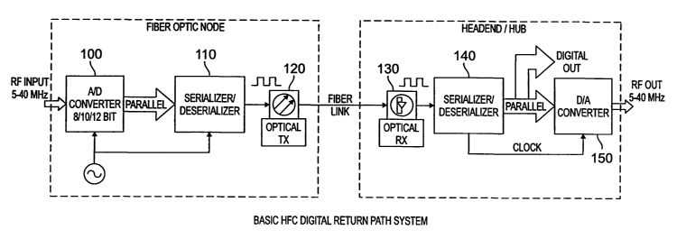
FIGURE 1 shows a block diagram of such a system. The system of
FIGURE 1 is described in detail under separate disclosure as noted above under
Cross-Reference to Related Applications. Essentially, the return path signal
from
the fiber optic node to the headend is represented by encoding it entirely as
ones
and zeroes. Specifically, the composite return path waveform is converted to a
sequence of digital words whose value represent analog signal samples (A/D
100),
the digital words are arranged into a serial stream with appropriate
synchronization
information (Serializer/Deserializer 110), and the electrical digital signal
is
converted into an optical digital signal and transmitted across the optical
fiber
(Optical TX 120). The optical path carries the signals to the headend which
has the
proper components for receiving and processing the optical signals, i.e., the
process
is inverted at the receive side (Optical RX 130, Serializer/Deserializer 140,
D/A
150). The use of this digital optical technology provides many key advantages
compared to traditional analog systems. Among these are longer distance
capability, performance insensitivity to length, environmental robustness,
cost
benefits, and interface flexibility.
The performance of digital return links can be compared favorably to their
analog counterparts. Additionally, the performance can be flexibly traded off
against bandwidth. This occurs by noting that less Analog-to-Digital (A/D)
converter bits of resolution used set the signal-to-noise ratio (SNR) for the
signal
being transported. Less bits to transport means lower SNR, but also a lower
data
-2-
CA 02400150 2002-08-14
WO 01/65732 PCT/USO1/06366
rate. More bits means a higher SNR at 6 dB/bit. As such, it is advantageous to
find
ways to improve the SNR after AlD conversion for lower resolution conversions.
If
the SNR can be increased by signal processing, a lower number of bits of
transport
can be used to meet a given SNR compared to the basic digital return system in
FIGURE 1. Such an approach fits broadly into the category of noise shaping
technology.
Improvement of CATV return path performance using cost effective
technologies is a primary issue in deploying reliable network architectures
for HFC.
In this regard, there is continued progress in the performance and speed of
state-of
the-art analog-to-digital converter (A/D) integrated circuit (IC)
manufacturers.
However, while it is straightforward to obtain a reasonable SNR at the receive
end
with high-speed off the-shelf A/D technology available today, HFC architecture
design involves more complexity than this single point-to-point example. In
practical hub and Headend environments, it is typically the case that received
inputs
from topologically diverse nodes are combined (RF summed) at the Headend. Each
such combine entails a noise penalty of 3 dB, or effectively decreases the
resolution
of the A/D system by one-half of a bit. In essence, a system designed with 10-
bit
A/D converter in the field, and combined four ways at the Headend, has the
theoretical performance of an 8-bit system. Similarly, if it is desired for
the end-of
line performance to have ten bits of resolution after a four way combine, then
the
conversion process must begin with 12 bits of theoretical performance at each
node.
-3-
CA 02400150 2002-08-14
WO 01/65732 PCT/USO1/06366
The present invention is therefore directed to improving the performance of
a CATV HFC baseband digital optical transmission return path using cost
effective
digital solutions.
SUMMARY OF THE INVENTION
A system for improving the performance of the HFC return path according
to the present invention implements a DSP approach to increase the signal-to-
noise
ratio (SNR), thereby improving the performance of the HFC return path without
resorting to higher resolution A/D converters. The approach uses well-known
signal processing architectures applied to an RF system to achieve in-band
quantization noise reduction. The technique is applicable to any HFC return
architecture that uses a baseband digital optical transmission in the reverse
path
implementation.
One exemplary embodiment of the present invention includes a
system and method for increasing the performance of a digital return path in a
hybrid-fiber-coax television system using baseband serial optical transport,
receives
an analog composite return path waveform at a comparator input to a digital
return
transmitter that includes an A/D converter and a first nonlinear processor. A
first
processing function is applied to a signal output from the comparator at the
first
nonlinear processor and the processed signal is forwarded to the A/D converter
which converts the processed signal to generate a quantized output signal of a
sequence of digital words whose value represent analog signal samples. The
quantized digital signal is output to an output of the digital return
transmitter and to
-4-
CA 02400150 2002-08-14
WO 01/65732 PCT/USO1/06366
a feedback loop including a D/A converter, which converts the quantized
digital
signal to an analog feedback signal and forwards the analog feedback signal to
a
second processor. The second processor applies a second processing function to
the
analog feedback signal and outputs the processed analog feedback signal to the
comparator input of the digital return transmitter. The comparator input to
the
digital return transmitter adds the processed analog feedback signal to the
analog
composite return path waveform to create the signal output from the
comparator.
In one embodiment of the invention the method further includes the step of
lowpass filtering the quantized digital signal and in yet a further
embodiment, the
step of downsampling the filtered quantized digital signal.
BRIEF DESCRIPTION OF THE DRAWINGS
The above-mentioned and other objects, features and advantages of the
present invention will become more apparent from the following detailed
description when taken in conjunction with the accompanying drawings, wherein:
FIGURE 1 depicts the basic elements of a hybrid fiber-coax digital return
path transport system.
FIGURE 2 depicts a simplified block diagram of a digital return transmitter
with nonlinear processor.
FIGURE 3 illustrates the quantization noise spectrum of an A/D converter
with noise-like input.
FIGURE 4 illustrates the shaped quantization noise spectrum vs.
unprocessed quantization noise spectrum.
-5-
CA 02400150 2002-08-14
WO 01/65732 PCT/USO1/06366
FIGURE 5 graphs the rms noise vs oversampling ratio and illustrates the
effect of nonlinear feedback on quantization noise performance.
FIGURE 6 depicts a simplified block diagram of a first sigma-delta A/D
converter including a first order modulator and a digital decimator.
DETAILED DESCRIPTION
The basic elements of the proposed system for improved return path
performance for digital communication signals are shown in FIGURE 2 which
shows an example topology of an A/D converter with additional functional block
diagrams which perform digital signal processing (DSP) algorithms designed to
improve the SNR compared to a system that does not perform the processing
functions. Implemented in the DSP is a nonlinear method, used in high-
performance applications such as audio processing, that create this
improvement.
The system shown in FIGURE 2 illustrates a processor and A/D converter in
which
an analog input signal A(s) is input to a comparator 10, the output of which
is
coupled to a nonlinear processor H(s) 20, the output of which is coupled to
A/D
converter 30. In a feedback loop, the output of A/D converter 30 is coupled to
a
D/A converter 40 and processor F(s) 50 in the feedback loop to the input
comparator 10. Essentially, the input to the circuit is fed to the quantizer
via the
nonlinear processor, and the quantized output is fed back through D/A
converter 40
which converts each sample of the digital signal to generate the analog
feedback
signal which is coupled and subtracted from the input, forcing the average
value of
the quantized signal to track the average input.
-6-
CA 02400150 2002-08-14
WO 01/65732 PCT/USO1/06366
Those skilled in the art will appreciate that implementation of this type of
converter is generally based on low-frequency implementations, such as for
high-
fidelity audio. Additionally, the quantization level is typically of lower
resolution
due to the ability to implement DSP more effectively at the low speeds
typically
used. For the CATV application, the implementation of the DSP algorithms is
significantly increased in complexity and design due to the nature of the high
speed
processing necessary.
With reference to FIGURES 3 and 4 , the operation of the processor is
discussed and the nature of the improvement provided by the implementation of
the
converter in the digital return transmitter is graphically shown. The
quantization
noise spectrum of the output of an A/D converter is shown in FIGURE 3. The
reverse path bandwidth is assumed identical to the Nyquist bandwidth at the
A/D
output B"1. As can be seen, the noise spectrum is modeled as flat over the
Nyquist
bandwidth of the converter. FIGURE 3 shows a sampled output spectrum with
typical relationships between the three parameters above. The higher the clock
frequency is relative to the reverse path bandwidth B"1, the lower the
spectral
density becomes, providing a means to lower the noise power in the reverse
bandwidth. FIGURE 3 shows this example where the clock frequency is increased,
going from B"1 to B"2, and lowering the spectral density. In other words, the
same
amount of noise power, determined by the resolution of the A/D, is spread over
a
wider Nyquist bandwidth.
This "oversampling" technique illustrated with reference to FIGURE 3 is an
inefficient way to obtain noise reduction, as the clock rate must be doubled
to
CA 02400150 2002-08-14
WO 01/65732 PCT/USO1/06366
achieve only 3 dB of SNR improvement. Additionally, the digital reverse system
for HFC is already implementing A/D converters that are operated at state of
the art
clock rates. It is not possible in commercial devices to increase the clock
rate
enough for major performance gains without suffering severe degradation or
rendering the part completely nonfunctional.
Instead of relying on oversampling alone to provide the increase in SNR,
FIGURE 2 shows a diagram of a nonlinear processor, H(s) which implements a
transfer function that provides this capability. Also, processor F(s) in the
feedback
loop may provide additional filtering as needed. Both H(s) and F(s) can take
on
many topologies, depending on improvement desired and complexity of
implementation. The nonlinear nature however makes precise analysis difficult,
especially when higher order architectures are used. In many cases behavior
may
only characterized through simulations.
An exemplary resulting noise spectrum from such a processor is shown in
FIGURE 4. In this case, the spectrum, which previously had a uniform density
(white) out to B", is no longer flat. The noise power between the uniform
density
and nonuniform density is the same, but in the latter case, the power is
shifted into
the region of spectrum between B"1 and B"2. That is, the modulator 'shapes'
the
quantization noise so that most of the energy will be above the signal
bandwidth.
Since the reverse system bandwidth is B"I, the region which now contains the
bulk
of the noise power can be filtered with no effect on the desired signal. 'Kith
much
of the noise now shifted into this region, the noise power within the
signaling band
has been reduced. This reduction of noise power is equivalent to the effect of
using
_g_
CA 02400150 2002-08-14
WO 01/65732 PCT/USO1/06366
a higher resolution A/D converter in that region of the sampled spectrum.
Since the
region of the sampled spectrum in which noise reduction occurs is the only one
of
concern, this technique essentially provides an effective bit increase
proportional to
the drop in noise power within B"1. In a representative example of what can be
expected, SNR improvements of 20 dB can be achieved, which corresponds to over
three bits of additional resolution. The exact gain is highly dependent upon
amount
of oversampling and the architecture of the nonlinear processor.
Mathematically, the noise reduction analysis can be expressed, in the most
simplistic case, using FIGURE 2 as a guide. Assume that F(s) = I. For
quantized
output Y(s), quantization noise Q(s), analog input A(s), and lowpass, high
gain,
processing transfer function H(s), the diagram shows the following:
Y(s) _ [A(s) - Y(s)] H(s) + Q(s) (1)
Y(s) + Y(s) H(s) = A(s) H(s) + Q(s) (2)
Y(s) = fA(s) H(s) / [I+H(s)]} + fQ(s) / [1+H(s)]} (3)
Then, assuming over the bandwidth of interest of the input that ~H(s)~ »l,
(3) becomes
Y(s) = A(s) + Q(s)/H(s) (4)
Because ~H(s)~ » l, the last term can be small. The quantization noise
spectral density, Q(s), is reduced by the magnitude of H(s) in the signal
bandwidth.
However, outside the signal bandwidth, the spectral density is increased. Of
course,
this part of the spectrum is of no interest. However, in order to make proper
use of
the shift in spectral energy to the high end of the band, digital filtering is
done after
the quantization process to reduce noise power (i.e. noise enhanced during the
-9-
CA 02400150 2002-08-14
WO 01/65732 PCT/USO1/06366
conversion process can be controlled very effectively). As illustrated in
FIGURE 6,
which shows a first sigma delta A/D converter coupled to a digital decimator,
a
digital lowpass filtering stage (lowpass filter 70) may be implemented to
smooth the
output of the digital modulator, greatly attenuating out-of band quantization
noise,
interference and high frequency components of the signal. Also, if desired,
downsampling (downsampler 80) can be implemented to bring the sampled signal
to the Nyquist rate.
As an example, consider an 8-bit A/D converter. This number is chosen
because it has practical implication in terms of both performance and speed
for the
HFC application. Today, a good off the-shelf 8-bit device samples at roughly
200
MHz, providing roughly a two-times oversampling for HFC return paths. Within
another year, the high-end parts available now that go faster will be
available in
volume and at low cost, suitable for CATV applications. A four-times
oversampling will be easily within reach.
FIGURE 5 plots the in-band noise against the oversampling ratio for
examples of PCM and one, two and three feedback loops. Referring to FIGURE 5,
it can be seen that a four-times oversampling with a second order feedback
system
provides roughly 20 dB of additional in-band quantization noise reduction. At
6
dB/bit, this represents more than three bits of effective resolution, turning
a 7.5-bit
conversion process (an 8-bit non-ideal A/D converter) into nearly eleven bits
of
effective resolution. This represents performance essentially better than any
analog
return technology in widespread use today, such as linear DFB laser
transmitters.
Additionally, unlike the linear optics case, the performance is distant-
independent.
-10-
CA 02400150 2002-08-14
WO 01/65732 PCT/USO1/06366
In terms of implementation, architectures such as those above where F(s)=1,
which represent delta-sigma modulation, are well suited to digital design
technologies, such as FPGA's and custom ASIC design. However, the clock rates
required to achieve the necessary oversampling ratio are relatively high for
commercial FPGA implementation in today's technology. Custom IC
developments have created chips capable of these processing rates. It is
anticipated
that the commercial FPGA hurdle also will be cleared in the near future as
development continues.
The above describes a DSP approach to increasing the performance of the
IO HFC return path without resorting to higher resolution A/D converters. The
approach uses well-known signal processing architectures applied to an RF
system
to achieve in-band quantization noise reduction. The individual components are
known and widely available. The technique is applicable to any HFC return
architecture which uses a baseband digital optical transmission in the reverse
path
implementation.
Although various embodiments are specifically illustrated and described
herein, it will be appreciated that modifications and variations of the
invention are
covered by the above teachings and are within the purview of the appended
claims
without departing from the spirit and intended scope of the invention. For
example,
referring once again to FIGURE 2, processor F(s), like processor H(s), can
take on
any variety of transfer function responses to serve application performance
requirements. Furthermore, this exemplary modification should not be
interpreted
to limit the modifications and variations of the invention covered by the
claims but
-11-
CA 02400150 2002-08-14
WO 01/65732 PCT/USO1/06366
are merely illustrative of possible variations.
-12-