Note: Descriptions are shown in the official language in which they were submitted.
CA 02400294 2002-08-15
WO 01/61400 PCT/USO1/05309
TWO-DIMENSIONAL MICRO-MIRROR ARRAY ENHANCEMENTS
j BACKGROUND OF THE INVENTION
The invention relates to optical networking
devices such as cross-connect switches and, more
particularly, to cross-connect switches that use
micromachined mirror arrays.
The huge bandwidth of optical fibers, in
combination with enormous growth of data and voice
traffic, has led to a significant amount of recent
development activity in the field of optical
communications. Advances have occurred in architectures
and network components, such as optical switches.
One approach to optical switching involves the
use of micro-machined mirror arrays. Prior efforts using
this approach, like those of other approaches, tend to
have certain shortcomings, such as limited scalability
and a relatively low level of integration.
SUMMARY OF THE INVENTION
In an aspect of the invention, a structure
includes a reference member having a raised portion
thereon, a mirror suspended above the raised portion and
driving devices disposed on the raised portion to impart
rotational motion to the mirror in two axes of direction.
In another aspect of the invention, a method of
fabricating micro-mirror structures in a micro-mirror
strip of micro-mirror structures includes forming a
CA 02400294 2002-08-15
WO 01/61400 PCT/USO1/05309
pyramidal structure from a substrate material and
defining electrodes on the pyramidal structure.
In yet another aspect of the invention, a
micro-mirror strip assembly includes a frame, an array of
two-dimensional deflecting mirrors mounted in the frame
and dams disposed between the mirrors to block viscous
interaction between each of the two dimensional
deflecting mirrors and adjacent ones of the two-
dimensional deflecting mirrors in the array.
In still yet another aspect of the invention, a
hinge includes a plurality of parallel hinge sections
provided by vertical slots therein, the slots and
parallel hinge sections being dimensioned to provide
vertical and lateral stiffness to and a minimal torsion
spring constant for the hinge.
Among the advantages of the present invention
are the following. The placement of the electrodes on
raised structures on a substrate provides for increased
electrostatic force, as well as enhanced instability,
thus lowering the required drive voltage and enhancing
the deflection angles of the mirrors. The slotted hinge
has high torsional flexibility and high stiffness (both
vertically and laterally). The dam feature overcomes the
undesirable effects of the interaction of the flow of air
from adjacent mirrors in a micro-mirror strip assembly.
Other features and advantages of the invention
will be apparent from the following detailed description
and from the claims.
BRIEF DESCRIPTION OF THE DRAWINGS
-2-
CA 02400294 2002-08-15
WO 01/61400 PCT/US01/05309
FIG. 1A is a top plan view of a micro-mirror
strip assembly.
FIG. 1B is a side view of the micro-mirror
strip assembly of FIG. 1.
FIG. 2 is a plan view of a single micro-mirror
structure having electrodes arranged on the conical
substrate.
FIGS. 3A and 3C are plan views of the micro-
mirror structure with alternative arrangements of
electrodes.
FIGS. 3B and 3D are schematic diagrams of servo
control arrangements for electrodes of FIGS. 3A and 3C,
respectively.
FIGS. 4A and 4B are schematic diagrams of
select circuits.
FIGS. 5A and 5B are side and plan views,
respectively, of the micro-mirror structure having
electrode structures integrated with mirrors using one
layer of silicon-on-insulator.
FIGS. 6A and 6B are depictions of different
shapes of platform structures.
FIG. 7 is a cross-sectional side view of a
micro-mirror structure fabricated with two layers of
silicon-on-insulator.
FIGS. 8A-8C are different views of s micro-
mirror structures including dam structures (FIGS. 8A-8B)
and added dam structures (FIG. 8C) to cancel viscous
interaction between the various mirrors.
FIG. 9 is top view of a micro-mirror structure
with integrated current sources and amplifiers.
-3-
CA 02400294 2002-08-15
WO 01/61400 PCT/USO1/05309
FIGS. 10A-10B are cross-sectional and top
views, respectively, of a micro-mirror structure having
drive amplifiers.
FIGS. 11A-11B are cross-sectional and top
views, respectively, of a micro-mirror structure having
drive amplifiers integrated with a substrate.
FIG. 12 is a top view of a mirror arrangement
having inner torsion hinges with steep mechanical
returns.
FIGS. 13A-138 are top views of bifold hinges.
FIG. 14A is a graph of torsional constant
versus aspect ratio
FIGS. 14B and 14C are views of a micromachined
hinge having vertical slots to reduce length while
maintaining its torsional constant (FIG. 14B) and a
detailed view of the slots (FIG. 14C), respectively.
FIGS. 15A-15D are illustrations of meander type
hinges with high vertical stiffness.
FIG. 16 is a plan view of a micro-mirror
structure in which the mirrors have one thickness and the
hinges have a different thickness.
FIGS. 17A-17D are top views of shear sensor
implementations.
FIGS. 18A-18C are different views of a portion
of a micro-mirror structure having a sensor shield layer.
FIG. 19 is a depiction of curvature of a mirror
due to electrostatic forces.
FIG. 20 is a cross-sectional side view of an
electrode/substrate structure having a resistive material
to minimize mirror arcing.
FIGS. 21A-21C are illustrations of a dense
-4-
CA 02400294 2002-08-15
WO 01/61400 PCT/LTSO1/05309
deflecting array as used in two-dimensional deflection
schemes and an air channel underneath the mirrors.
FIGS. 22A-22E are illustrations of dams used in
the two dimensional mirror arrays to prevent interaction
between the mirrors.
FIG. 23A-23E are illustrations depicting a
spacer configured to reduce buildup of pressure in an air
channel.
FIGS. 24A-24B are illustrations of the use of
rotated deflection axes to shunt resulting airflow
between adjacent mirrors.
FIG. 25 is a depiction of a substrate with
separated mirror strips to improve temperature matching.
FIGS. 26A and 26B are plan and side views,
respectively, of a micro-mirror strip assembly using a
magnetic drive arrangement for controlling mirror
movement.
FIG. 27 is an illustration of a mirror
arrangement for reducing the distance of collimators to
their target mirrors.
FIG. 28A is a side view of a micro-mirror strip
assembly having plated, conical (or quasi-conical)
electrodes.
FIG. 28B is a top plan view of the micro-mirror
strip assembly of FIG 28A showing a single, plated
electrode structure.
DETAILED DESCRIPTION
With reference to FIGS. lA-1B, a micro-mirror
strip assembly 10 includes a plurality of micro-mirror
-5-
CA 02400294 2002-08-15
WO 01/61400 PCT/LTSO1/05309
structures 12, each of the micro-mirror structures 12
including a mirror arrangement 14 disposed above and
supported over a top surface of a reference member or
substrate 16. As shown in FIG. 1A, each mirror
arrangement 14 includes a mirror 18 coupled to mirror
frame 20 by a first pair of torsion members 22a, 22b. The
mirror arrangement 14 further includes a second pair of
torsion members 24a, 24b, which couple the mirror frame
20 to strips 26.
Referring to FIG. 1B, the substrate 16 includes
a base portion 28, a raised portion 30 on the base
portion 28, and sidewall portions 32 on either side of
the base portion 28. The substrate may be made of
ceramic or other suitable materials. The strips 26 are
located on top of the sidewalls 32. As shown by the
raised portion 30 (FIG. 1A), the raised portion 30 is
conical or quasi-conical in shape.
Electrodes 34 are disposed on the surface of
the raised portion 30 to impart a rotational motion to
the mirror 18 and the mirror frame 20 (shown in FIG. 1A).
The electrodes 34 control the inner rotation of the
mirror arrangement around the torsion members 22a, 22b
("x-axis"), as well as control the outer rotation of the
mirror arrangement around the torsion members 24a, 24b
("y-axis"). Although the raised portion 30 has been thus
described as having a cone or cone-like form, it may take
any shape or structure that allows the electrodes 34 to
be positioned close to the mirror arrangement 14 and
support rotational movement of the mirror arrangement in
the x-y plane.
Preferably, the mirror arrangement 14 and the
-6-
CA 02400294 2002-08-15
WO 01/61400 PCT/CTS01/05309
electrodes 34 are so positioned relative to the cone 30
such that the cone 30 is centered approximately under the
mirror 18. Substrate areas beneath the mirror frame 20
need not be conical, but may be sloped on such an angle
as required to allow the mirror arrangement 14 to rotate
freely through its outer axis of rotation around torsion
members 24a, 24b. These substrate areas can be machined
linearly in the substrate 16, thus simplifying the
fabrication of the substrate 16.
As can be seen in FIG. 1B, a spacer 35 can be
used between each of the strips 26 and the sidewall
portions 32 of the substrate 16 below such strips 26.
Typically, spacers in conventional micro-mirror
structures having planar substrates are on the order of
IS 150 microns. The spacer 35 of the micro-mirror structure
12 cad be as thin as 25 micron or even less, or could
even be eliminated altogether, given the effective
separation between the electrodes and mirror arrangement
as determined by the cone-like shape of the raised
portion 30. Also, because that separation is smaller and
more uniform, the maximum electric field can be reduced,
improving the protection against breakdown. The angles
in the bottom of the substrate 12 are not critical.
Typically, because the substrate 16 is made in sections
of 4.5" x 4.5", the sections are all made together. The
substrate material may be machined in vertical and
horizontal directions to remove material under a desired
angle. The cone or cone-like shape is ground on the top
to complete the substrate structure or can be etched into
the substrate surface. Alternatively, a mold may be made
to cast the substrate material in a green state.
CA 02400294 2002-08-15
WO 01/61400 PCT/USO1/05309
There are alternatives to forming a raised
portion on the substrate. One such alternative is
described later with reference to FIG. 28.
Thus, as introduced above, and shown in FIG. 2,
the electrodes 34, shown here as four electrodes 34a,
34b, 34c, 34d, are disposed on the cone 30 to deflect the
mirror arrangement 14 in both axes. Since the mirror
arrangement 14 is near the substrate 12, enhanced
electrostatic forces allow the use of smaller deflection
plates for the electrodes such that the mirror is easily
deflected in both axes. As will be described, a first
sensor controls the deflection in one axis and second,
another sensor controls the deflection in the other axis.
Thus, with the particular positioning of the electrodes
34, there is a stronger interaction between axes under
the control of the sensors. Additionally, a small DC
bias can be applied to the electrodes to render the
mirror inherently unstable. Since the position of the
mirror is unstable without the application of a servo
signal even when the applied driving signal is zero, a
large deflection with relatively small imposed driving
signals is therefore possible.
Referring to FIG. 3A, the micro-mirror
structure 12 (of FIG. 1A) further includes two torsion
sensors, a first torsion sensor 36 and a second torsion
sensor 38. The first torsion sensor 36 is located in one
of outer torsion members 24, specifically the torsion
member 24a, and detects outer axis rotation in the
direction of arrow 37. The second torsion sensor 38 is
located in one of the inner torsion. members 22,
specifically the torsion member 22a, and detects inner
_g_
CA 02400294 2002-08-15
WO 01/61400 PCT/USO1/05309
axis rotation in the direction of arrow 40).
The torsion members 22, 24 are depicted as
bifold hinges, but may be implemented with other types of
devices, as will be described later. The four deflection
plates or electrodes 34 (not shown) are arranged in
quadrant form, with the letters "A", "B", "C" and "D"
being used to represent the underlying electrodes 34a,
34b, 34c, 34d in corresponding quadrants 42a, 42b, 42c
and 42d (shown in bold). Increasing voltage applied to
both B and C and decreasing the voltage applied to A and
D produces rotation along the outer axis 37. Likewise, a
voltage decrease in both A and B, and a voltage increase
in D and C produces rotation along the inner axis 40.
The sensors 36, 38 produce signals when rotation occurs
along either the outer axis or inner axis. Hence, the
output of torsion sensors 36, 38 may be used to produce
stable electrostatic servo control. It will be
appreciated that, in this particular embodiment, the
organization of or quartering of the electrodes into four
electrodes in four corresponding quadrants is along lines
parallel to the rotation axes 37, 40.
Referring to FIG. 3B, a servo control system 50
includes summing amplifiers 52a, 52b, 52c, 52d connected
to and followed by high voltage amplifiers 54a, 54b, 54c,
54d to drive the deflection plates (indicated by A, B, C,
D), respectively. Preferably, the plates A, B, C, D are
DC biased with a bias voltage near the middle of the
supply range to linearize the drive characteristics so
that the net torque on the mirror is zero when the mirror
is at rest and not angled. If the four deflection plates
are sitting on a cone, the mirror may be made inherently
-9-
CA 02400294 2002-08-15
WO 01/61400 PCT/USO1/05309
unstable along either or both axes. The respective
outputs of the torsion (shear) sensors 36, 38, indicated
as 58 and 60, respectively, are provided to all four
plates (via the amplifiers 52 and 54), but with different
weights for different plates. The amplifier 52a has at
least 3 inputs: an offset voltage 56a that produces the
bias voltage to linearize the servo control, the inverted
output of sensor 36 (input 62) and the inverted input of
sensor 38 (input 64). These sensor feedback voltages may
have different gains applied to them, as indicated by R2
and R3, to account for the effects of different torques
around the different axes 37, 40.
By the same arrangement, the amplifier 52b
receives a DC bias 56b, an input for sensor 36 (input 58)
and the inverted input from sensor 38 (input 64),
adjusted with the appropriate weights to produce the
desired output. The electrodes represented by C and D
are driven in similar fashion. Since the outputs of both
sensors 36, 38 interact with all four plates A, B, C, D,
additional feedback between the control loops of the axis
37 and axis 40 may be required to optimize the control.
The sign of the sensor feedback voltages is adjusted as
necessary to give correct feedback.
The servo control arrangement of FIGS. 3A-3B
can be used with planar electrodes, but is particularly
advantageous when the electrodes are placed on a conical
or quasi-conical substrate like that shown in FIGS. 1A-
1B. The torsion sensors 36, 38 (from FIG. 3A) may be of
the four terminal type, or may be a resistor bridge
arranged to measure shear.
Referring to FIG. 3C, in an alternative
- 10-
CA 02400294 2002-08-15
WO 01/61400 PCT/USO1/05309
arrangement of the micro-mirror structure 12, the
electrodes 34 are divided among the diagonals of the
rotation axes 37 and 40. That is, the organization of or
quartering of the electrodes into four electrodes in four
corresponding quadrants occurs at a 45 degree angle
relative to the rotation axes 37, 40. The sensor 38
predominantly controls the output of plates B and D, and
the sensor 36 predominantly controls the output of plates
A and C. To increase torque along the axis 37, the
plates B and D may also be used, by increasing the
voltage to both plates simultaneously. Increasing the
voltage to both of plates B and D simultaneously serves
to increase the tilt of the plate in the direction in
which it is already tilted. Likewise, increasing the
voltage to both A and C increases the tilt around the
axis 40 in the direction in which it is already tilted,
since the mirror section is closer to the plates. Hence,
when feedback is used from these plates around either
axis, it must be weighted with the sign of the rotation
around that particular axis. This is schematically
illustrated in FIG. 3D.
Referring now to FIG. 3D, in a servo control
system 50' for the alternative arrangement of the
electrodes, the inputs take into account the new
orientation of the plates with respect to the sensors.
For example, plate C has as inputs the bias voltage, the
output from the sensor 36 and the signal from the sensor
38, weighted with the sign of the rotation around the
axis 40, to produce the correct feedback from the sensor
38. Likewise, the plate A is weighted with the same
inputs, but the sign of the sensor 36 is inverted.
CA 02400294 2002-08-15
WO 01/61400 PCT/US01105309
Again, the weights (i.e., the ratios of the resistors)
for different plates may be individually adjusted. Note
that in either of the arrangements of FIGS. 3A and 3C,
the plates A, B, C, D may be arranged to cover the mirror
18, or both the mirror 18 and the surrounding mirror
f rame 2 0 .
It is possible to reduce the number of leads to
each of the torsion sensors 36, 38. Referring to FIG.
4A, a torsion sensor select circuit 70 connects a current
source 72 to one of the sensors 36 or 38 using enabling
lines 74, which carry a voltage of e.g., OV for enable
and +10V for disable. 74, The sensor select circuit 70
couples outputs for the selected one of the sensors 36,
38 to respective forward biased diodes 76, 78, and an
instrumentation amplifier 80. The output signal produced
by the instrumentation amplifier 80 is provided to the
servo control system.
Alternatively, and as shown in FIG. 4B, a
torsion sensor select circuit 70' includes a set of
MOSFET or FET transistor switches 82, 84. In this
arrangement, current sources 72 are always active, but
the outputs of only one of the sensors 36, 38 are
selected by activating the respective switches 82, 84
using a select signal on select line 86. In the
exemplary torsion select circuits 70 and 70' of FIGS. 4A
and 4B, respectively, the diodes or switches and
connections may be integrated with the mirrors on the
silicon substrate.
Referring to FIGS. 5A and 5B, a micro-mirror
structure 90 disposed on a single silicon-on-insulator
(SOI) structure is shown. The structure substrate is
- 12-
CA 02400294 2002-08-15
WO 01/61400 PCT/USO1/05309
comprised of silicon. During fabrication of the
structure, a wafer 92 is etched to various depths to
provide the conical or quasi-conical form of the micro-
mirror structure of FIG. 1A. The different masking steps
94 may be achieved by using either isotropic or
anisotropic etching. After the definition of the
electrode step geometry, the electrodes 96 are defined.
The electrodes 96 may be made by junction isolation, or
may be deposited on top of an insulating oxide or other
insulators. The metal may comprise a suitable high
temperature refractory type metal such as tungsten, or a
metal silicide.
Referring to FIG. 5B, the electrodes 96 (of
which only one is shown) can be arranged in a quad pair
or as sets of separate x and y electrodes. Referring
again to FIG. 5A, after completion of structures 94 and
the placement of electrodes 96 thereon, a second wafer 98
is bonded to the wafer 92 by conventional wafer bonding
techniques, or other suitable techniques. The second
wafer 98 may also be an SOI wafer, preferably with the
device side facing the wafer 92. The second wafer 98 is
lapped down to a desired thickness. The sensors and the
mirror patterns are defined by reactive ion etching.
After the definition of the mirror (and torsion sensors)
100, a layer of a metal e.g., gold is evaporated to
produce the mirror 100. It should be noted that an oxide
layer 102 between the two wafers (layers) 90, 98
separates the mirror 100 from the structures of the
underlying substrate, that is, the wafer 92.
The term "pyramidal steps" as used herein
refers to the steps 94 which give rise to a generally
-13-
CA 02400294 2002-08-15
WO 01/61400 PCT/C1S01/05309
conical formation (which, as earlier noted, allows the
mirror to pivot around two axes, i.e., two-
dimensionally). For example, the steps 94 may be
hexagonal or octagonal, or any shape that approaches a
conical shape, e.g., the steps may be round circles
rather than polygons. The steps (or platforms) 94 having
polygonal shapes are shown in FIGS. 6A and 6B. FIG. 6A
illustrates hexagonal shaped platforms 94. FIG. 6B
illustrates octagonal shaped platforms 94. With such
shapes, the electrodes and the mirror axes are preferably
positioned so that the axes do not coincide with the
vertices of the electrodes, thus minimizing vertex
effects.
The required slope can be achieved by etching a
number of steps of varying depth, providing a pyramidal
arrangement that improves the deflection of the substrate
and lowers the required voltage as described above.
Referring to FIG. 7, an alternative a micro-
mirror structure 110 is constructed using a dual layer
SOI structure. The steps 94 in the structure 110 are
defined in an intermediate layer 112. The intermediate
layer 112 is another SOI layer of a desired thickness.
The electrodes 96 are defined and provided as described
above with respect to FIG. 5A. In the dual layer SOI
structure, there are two layers of oxide, a first oxide
layer 102 and a second oxide layer 114, separating the
various layers of silicon. After the formation of the
steps 94 and the definition of the electrodes 96, the
second wafer 98 is bonded to the intermediate layer 112
and wafer 92, and is then lapped down to the required
mirror thickness, to form a top layer. Implantation and
-14-
CA 02400294 2002-08-15
WO 01/61400 PCT/USO1/05309
definition of the sensors, followed by reactive ion
etching of the mirrors 100 and gold evaporation defines
the mirror and its hinges.
The fabrication techniques of FIGS. 5-7 allow
for the incorporation of dams between adjacent mirrors to
reduce interaction of viscous flow of one mirror with the
adjacent mirrors, as will be described further with
reference to FIGS. 8A-8C. Referring to FIG. 8A, in yet
another depiction of a strip assembly 115 of micro-mirror
structures, etching is performed to produce a single
platform 94, either raised or recessed. A set of
electrodes 96 (either a quad set as shown or separate
sets of x and y electrodes) is diffused in the surface of
that platform 94.
Referring to FIGS. 8A-8C, etching of one or
more steps 94 in a silicon substrate provides a natural
dam for blocking interaction between adjacent mirrors,
either for pyramidal electrodes (as illustrated in FIG.
8B) or for the single cavity (as illustrated in FIG. 8A).
The dam action is can be described with reference to FIG.
8C, which provides a length-wise, cross-sectional view of
the strip assembly 121.
Referring to FIG. 8C, interaction between the
mirrors 100 is almost completely blocked by dams 122.
Additional blocking dams 124 formed above the silicon
substrate (as illustrated in the figure) may be used.
The increased height of the dam resulting from a
combination of the dam 122 and the blocking dam 124 thus
further improves isolation. The blocking dams 124 may be
constructed using dry resist or Vacrel. Moreover, each
blocking dam 124 may be made very narrow by etching with
-15-
CA 02400294 2002-08-15
WO 01/61400 PCT/CTSO1/05309
Reactive Ion Etching (RIE), leaving a high but thin
structure of very high aspect ratio.
It is worth noting that the dams 122 (alone or
in combination with the blocking dams 124) also serve to
strengthen the already existing shield of driving fields
in the electrodes regions as provided by the surrounding
silicon. Thus, the dams 122 provide various types of
isolation, including electrical.
In all of the structures of FIGS. 8A-8C, it is
possible to integrate the driving amplifiers or torsion
sensor amplifiers in one of the silicon layers that are
present. It is also possible to further integrate the
electronics of the micro-mirror structure by integrating
current sources and sense amplifiers in the silicon next
to the sensors, thereby greatly reducing the capacitive
coupling to the driving leads.
Referring to FIG. 9, a micro-mirror structure
with integrated current sources and sense (or
instrumentation) amplifiers 130 is shown. In the
structure 130, a first hinge sensor 132 has an adjacent
sense amplifier and current source 134 attached,
integrated into the substrate, and a second hinge sensor
136 has an sense amplifier and current source 138
attached, also integrated in the substrate.
Alternatively, the sensor amplifier and current source
138 may be positioned closer to the hinge 136 by being
made part of the frame 20 itself, as the frame 20 is made
of single crystal silicon. Consequently, the sensor
leads are much shorter and immediately buffered by the
instrumentation amplifiers, thus greatly reducing the
capacitive coupling.
-16-
CA 02400294 2002-08-15
WO 01/61400 PCT/CJSO1/05309
Similarly, the electrostatic driver amplifiers
for the electrode may be integrated in the top silicon
layer, or in the substrate itself if the substrate is
made from silicon.
Referring the FIGS. 10A and 10B, a mirror
structure having integrated driver amplifiers 135 is
shown. In the mirror structure 135, the mirror 100 in
the top silicon layer 98 is positioned above the
substrate 92, which is also made out of silicon and which
has steps 94 as earlier described. The electrodes 96 (of
which only one is shown) are deposited on the substrate
92, and are driven by driving amplifiers 140 located in
the silicon substrate 92. Spacers 142 separate the top
silicon layer 98 from the substrate 92. Although not
illustrated, the two silicon layers 92, 98 are connected
with flip chip leads that connect the sensors or sense
amplifiers to the underlying substrate 92. Thus, the
sense amplifiers could also be located on the substrate
92.
Alternatively, if the electrode drivers are
integrated in the top silicon wafer, which incorporates
the sensors and the sense amplifiers, the substrate
itself may be made of ceramic. This type of structure is
illustrated in FIGS. 11A and 11B.
Referring to FIG. 12A, the substrate 92 has a
cone or pyramid 142 etched into it. A set of four
electrodes 94 (only one is shown in FIG. 11B) are
deposited on the cone 142. The driving amplifiers and
sensing amplifiers, represented collectively by reference
numeral 144, are now located on the top layer 98, which
is mounted in flip-chip fashion to the underlying
-17-
CA 02400294 2002-08-15
WO 01/61400 PCT/USO1/05309
substrate 92.
With any of these arrangements, the number of
leads needed for connections to external cables is
substantially reduced. However, some of the electronic
components, e.g., may be located on external boards along
with other servo control devices. The location and
partitioning of the various functions is based on the
estimated reliability of each component, and possibly
other factors e.g., cost.
A number of different devices may be used for
the inner and outer torsion members 22a-b, 24a-b,
respectively, from FIGS. 1, 2, 3A and 3C. For example,
and as shown in some of those figures, the device may be
a folded hinge such as a bifold hinge. An exemplary
bifold hinge is described in PCT Application Ser. No. 99
21139 and U.S. Patent Application Ser. No. 09/388,772,
which is incorporated herein by reference.
Returning briefly to FIG. 3A, the torsion
sensors 36 and 38 are positioned on the outside location
of the hinge with which they are associated so that that
hinge's leads do not need to be brought out over thin
portions of the hinge. Such positioning on the inner
hinges leads to a configuration in which the mechanical
return of the hinge to the mirror is located away from
the mirror. The resulting wide notch in the frame with
the mechanical load of the electrostatic attraction tends
to bend the outer frame 20, which is undesirable.
Referring to FIG. 12, a structure 150 using an
alternative bifold hinge 154 that avoids the bending of
the outer frame 20 under the electrostatic forces applied
-18-
CA 02400294 2002-08-15
WO 01/61400 PCT/USO1/05309
to both of the central mirror 18 and the outer frame 20
is shown. The bifold hinge 154 includes a mechanical
return 156 that is formed to be very steep towards the
mirror 18 while at the same time preserving the stiffness
of the hinge. Bending that occurs will occur primarily
in the hinge itself, and bending of the outer frame 20 is
thus minimized.
Mode characteristics of the folded hinge can
also be improved by tying various parts of the folded
hinge together with another hinge having characteristics
that differ from those of the folded hinge, as will be
further described with reference to FIGS. 13A and 13B.
This type of tying arrangement makes it possible to
maintain a torsional constant without incurring a
substantial increase in vertical stiffness.
Referring to FIG. 13A, an assembly 160 includes
a fixed part 162 and a movable member 164, which are
connected to one another by a folded hinge 166. The
folded hinge 166 includes a first flexure 168 and second
flexures 170, coupled by inner member 172 and outer
members 174, which may be completely stiff. Optionally,
the assembly may further include a torsion sensor 176 to
measure the deflection of the rotating hinge. Because
the hinge 166 is folded, it takes up much less space. In
addition, the hinge 166 has virtually the same torsional
constant as it would if members 170 and 176 were linearly
connected (without folding). The vertical stiffness may
be enhanced by as much as a factor of 4 because the
length (as compared to an unfolded hinge) is reduced in
half, which would increase the vertical spring constant
by a factor of 8. At the same time, however, there are
-19-
CA 02400294 2002-08-15
WO 01/61400 PCT/C1S01/05309
two springs in parallel, which provides in total
stiffness improvement of a factor of 4 (and hence a
doubling of the vertical resonance frequency). The hinge
of FIG. 13A as described thus far is similar to that
described in U.S. Patent Application Ser. No. 09/388,772.
It is understood that if points ~~a" and ~~b" are
linked so that they rotate freely, but are constrained
from moving vertically with respect to each other, then
the vertical stiffness would be further improved by a
factor of 2. This would require an ideally flexible
spring, but a good approximation can be obtained by using
a folded flexure hinge in its place. It is, of course,
possible to put a simple flexure in place, but a folded
hinge has better characteristics. It is desirable to
provide a hinge that is very flexible in rotation, but
stiff in vertical bending (the lateral modes are usually
of less importance as they are generally not excited by
the driving mechanisms).
It turns out that the characteristic for
torsion allows such hinges. By making the width of the
hinge narrow, thinner than the thickness, it now becomes
very flexible in torsion. By making it short, it can be
made vertically very stiff even if the width is reduced.
The vertical stiffness decreases as the third power of
the length, whereas the vertical stiffness only decreases
linearly with width. The torsional stiffness, however,
decreases as the third power of the width of the ribbon,
when the width is smaller than the thickness. Hence,
this indicates that the width should be smaller than the
thickness.
Referring to FIG. 13B, an assembly 180 includes
-20-
CA 02400294 2002-08-15
WO 01/61400 PCT/USO1/05309
a folded hinge 182 having points a and b connected with
simple, flexure hinge 184. The flexure hinge 184 may be
very narrow and slender, but quite long, thus giving a
very low torsion constant as well as very good vertical
stiffness. The hinge 184 may extend partially into
supports 172 and 164 for greater length and hence more
flexibility without affecting the operation of the
assembly. Flexure hinge 184 may be replaced by a
composite hinge such as the one illustrated in FIG. 13A.
It is highly desirable to have a micromachined
flexible hinge that is very short but still has very high
torsional flexibility. Also it is extremely desirable to
maintain torsional flexibility while maintaining high
vertical and lateral stiffness of the hinge. Folded
hinges provide one way of achieving this goal. A
different option is discussed below, with reference to
FIGS. 14A-14C.
Referring to FIG. 14A, a graph of the torsional
constant of a torsion bar for varying width to height
aspect ratios is shown. The graph illustrates the
variation of the torsion spring constant with varying
width to height ratios. For a rectangular cross-section
hinge, with a variable aspect ratio as illustrated, the
torsional constant of the hinge increases almost linearly
with the width when the width to aspect ratio is greater
than one and decreases approximately as the third power
of the width below that.
Referring to FIGS. 14B and 14C, consider now a
slotted hinge 190. The slotted hinge 190 includes narrow
verticals slots 191 (three being shown in greater detail
in FIG. 14C), cut in the silicon hinge 190 all the way
-21 -
CA 02400294 2002-08-15
WO 01/61400 PCT/USO1/05309
through as indicated and as shown in the cross-section
194. The net result is to form a set of hinges 192 which
are all in parallel, and each individual hinge 192 having
a much lower torque-constant than the original undivided
hinge. For example, each hinge 190 which has an aspect
ratio w/t of 2 to start with is divided into 8 parts by
slotting, and each of the sub-hinges 192 has an aspect
ratio 1~. The torsional stiffness of each of the sub-
hinges 192 per unit length is reduced by a factor of
almost 100, although 8 of them are placed in parallel.
Thus, a dramatic reduction in hinge stiffness can be
achieved in this manner. Micromachined hinges of this
type may be readily fabricated by deep reactive ion
etching using the Bosch or any other process which is
capable of making very narrow grooves of very high aspect
ratio. Hence, the hinge is masked off with oxide or any
suitable mask, and the vertical slots are simply etched
through the full thickness. Other etching methods may
also be used. The hinge material may be silicon,
polysilicon or any suitable oxide nitride, metal or any
material used in silicon device fabrication. The length
of the slot may be tailored to give the desired torque
characteristic. Of course, it is desirable for the slots
191 to be spaced as close together as possible. Hinges
192 may all be interconnected with a section 196 which as
seen in the cross-section 197 has no slits. The hinge
190 may include a torsion sensor 198 (bridge or four
terminal), could be implemented without the torsion
sensor 198 as well.
Such hinges maintain the vertical and lateral
stiffness that is desired. It is clear by inspection
-22-
CA 02400294 2002-08-15
WO 01/61400 PCT/C1S01/05309
that the vertical bending moment has been nearly fully
maintained since the beams add simply in parallel in that
direction. At the same time, their length has been
drastically reduced, which increases the spring constant
as the inverse third power of their length. The lateral
bending moment has in this case been reduced by a factor
of 64 due to the sectioning, but the reduction in length
compensates greatly for this decrease. Generally, the
lateral stiffness is somewhat less important than the
vertical stiffness, and given the dimensions of the hinge
that are typically involved, it is substantially larger
than the vertical stiffness to start with. Therefore, a
hinge having sections which are very narrow (like hinge
190 of FIG. 14B) may have the same torsional constant as
one that has many times its length, and its vertically
and laterally much stiffer.
Referring now to FIG. 15A, a meander-type hinge
200 includes torsion hinges 201 and 202, which are
connected by bands (springs) 204 and 206. In some
instances, it may be desirable for a micro-machined hinge
to provide design flexibility in a physical direction
that is different from the torsion hinge. The bands 204
and 206 are connected with ends 208 and 210. In such an
arrangement, it is important to keep the ends 208 and 210
tied together vertically to hold the vertical deflections
to a minimum and maximize vertical stiffness.
As illustrated in FIG. 15B, under torsional
load, both springs 204 and 206 deform and their ends are
tilted with respect to each other. If the ends 208 and
210 are tied together by a simple plate, then the
torsional spring constant is increased by almost a factor
- 23 -
CA 02400294 2002-08-15
WO 01/61400 PCT/USO1/05309
of 3. Hence, it is desirable to let the ends of springs
204 and 206 rotate with respect to each other, while
typing them together vertically.
Referring to FIG. 15C, the ends of the springs
204 and 206, shown as ends 212a and 212b, respectively,
are connected by a torsion hinge 214, which is very
flexible rotationally, but vertically stiff. Preferably,
the torsion hinge 214 is of the serrated type, as
illustrated in FIG. 15D and described above with respect
to FIG. 14B, which is very flexible but has high vertical
stiffness.
Alternatively, it may be of the folded hinge
type, as illustrated in FIGS. 13A-B and described in the
above-referenced PCT Application Ser. No. 99 21139 and
U.S. Patent Application Ser. No. 09/388,772. Any hinge
that has good vertical stiffness and good torsional
flexibility may be used for hinge 214.
For large mirrors, it is important that the
mirror be very flat, and hence it should be made of an
SOI silicon plate that is as thick as possible. The
hinges, made from the silicon layer, need to be very
flexible and may be much thinner than the mirror. The
mirror frame should be as sturdy as possible. These
different thickness requirements make it difficult to do
the lithography for sensors on hinges when there are
large depth differences. Thus, it is suggested that up
to three different thicknesses be used to fabricate the
scanner. These thicknesses may all be made by timed
anisotropic etching from the front, leaving the mirror
surface intact. A technique for two different
thicknesses is described in U.S. Patent Application Ser.
-24-
CA 02400294 2002-08-15
WO 01/61400 PCT/C1S01/05309
No. 09/446,540, incorporated herein by reference.
Referring to FIG. 16, in the micro-mirror
assembly 12 (again, shown in partial view for purposes of
simplification) the mirror 18 may be made of one
thickness, e.g., 15 micron; the hinges 22 and 24 can be
made of a different thickness, e.g., 7 micron, which may
produce a large step at the intersections 220 of the
hinges 22, 24 and the mirror plate 18, but no sensor
leads need to be bought out over this step on the inner
hinge 22. The outer frame 20 may be made, e.g., out of
10 micron, such that it has sufficient stiffness. At
location 222, where the leads for the inner sensor 36
need to be brought out, there is only a 3 micron step,
which is relatively easy to bridge. In fact, if the
outer frame 20 is made of the same thickness as the hinge
22, then there is no step at all.
Likewise, a step occurring at location 224 near
the outer hinge 24 is relatively small, and is easily
crossed. At location 226, near the sensor 36, there is
usually a return to the full plate thickness, but the
leads in this area can be far spread out so that only
thick lines have to go across the step.
To reduce the inertia of the mirror 18, it is
possible to make the frame 20, e.g., 15 micron thick,
while making the mirror 18 only 7 micron thick. This is
similar to the etched frame described in U.S. Patent Ser.
No. 5,629,790. All of these structures can be made of
SOI silicon as described above or polysilicon, which has
been etched from the top surface.
Referring to FIG. 17A, a shear sensor 230
- 25 -
CA 02400294 2002-08-15
WO 01/61400 PCT/USO1/05309
integrated in a torsion hinge is shown. A current sent
through current contacts 232 produces a differential
signal on the sensing electrodes 234 in an implant region
236 when shear is applied in the plane of the sensor 230.
The ratio of the width of the current contacts 232 to the
length of the sensor is usually between .8 and 2. A
vertical offset in the mask for the current contacts 232
produces an offset voltage on the electrodes 234. The
offset voltage is defined as the sensor output for a
given current when there is no stress to the transducer.
Referring to FIG. 17B, the current contact 232
is widened and is wider than the current path in the
sensor proper; any vertical or even horizontal
misregistration now has very little effect on the sensor
output and hence on the offset of the sensor. Current
contacts 232 are located inside the recesses 236 of the
implant region 236 that defines the sensor 230. The
widened contact also lowers the required current density
on the electrodes 234, which in turn makes current
density more uniform. Current non-uniformities in the
contacts caused by local effects tend to be evened out
with this arrangement.
With reference to FIG. 17C, to further improve
the shear sensor and its offset, insulating dams 238 are
placed in the implant region 236, as is sometimes done
for Hall effect devices. The insulating dams 238 produce
a restriction of the current (with a subsequent
expansion) and eliminate much of the discontinuities
since the current is now almost fully lithographically
defined. The insulating dams 238 are used to constrict
the current from electrodes 234 in the implant region
-26-
CA 02400294 2002-08-15
WO 01/61400 PCT/IJSO1/05309
236.
The insulating dams mechanism described above
in reference to FIG. 17C is a measure that may be taken
to decrease the offset voltage between the sensor
electrodes 234. However, in some cases, it may be
desirable to produce a unipolar offset which is well
calibrated on top of the random offset that is caused by
the remaining uncontrolled non-uniformities and
lithographic misregistrations.
Referring to FIG. 17D, the electrodes 234 are
deliberately offset in a vertical direction, thus
producing a known offset voltage. Consequently, the
output of the sensor is always biased to one side, a
result that may be desirable for some calibration
procedures. The offset may also be produced by a lateral
displacement of the electrodes 234.
Referring to FIG. 18A, a shielded sensor
structure 240 is shown. The structure 240 includes a
silicon layer 241, an insulating layer 242, a metal layer
243. The structure further includes a sensor implant
resistor 244 in the silicon layer 241 that is coupled to
the metal layer 243 and a shield 245 that is applied over
the sensor implant resistor 244 to stabilize sensor
output and eliminate light sensitivity. While silicon is
normally not sensitive to light in the telecom
transmission region (wavelength > 1.3 micron), during
alignment if visible or near visible light is used, it is
possible to induce small transients in the sensor. These
small transients may give rise to erroneous calibration.
The shield 245, together with the insulating layer 242 (a
layer of oxide, nitride or oxy-nitride), provides a
-27-
CA 02400294 2002-08-15
WO 01/61400 PCT/USO1/05309
substantial protection against drift or source
contamination, and also protects to some degree against
the driving electrostatic field.
FIG. 18B provides a top view of the sensor
structure 240. As shown, the shield 240 may be tied to
ground (e.g., on one end of the current source) or to a
fixed potential. Referring to FIG. 18C, in an
alternative arrangement, the shield 240 can cover the
sensor implant resistor 244 completely. The contacts for
the sensor implant resistor 244 are made through highly
doped implant contact regions 246.
Referring to FIG. 19, mirror curvature as a
function of loading 250 is shown. It is recognized that
thin electrostatic mirrors may bend under the forces of
the electrostatic field that is used, particularly if the
mirrors are very large. A mirror 252 in a rest position
(indicated by line 0 - 0') is capable of bending towards
electrodes 254 under the electrostatic forces. When the
same voltage bias is applied to both of the electrodes
254, the deflection may be moderate, as illustrated by
the curve 1 - 1' (e. g., a fraction of 1/10 micron). When
the mirror gets deflected, the load is increased on one
side and decreased on the other, but the net effect is
that the average bending is increased, as illustrated by
curve 2 - 2'. This curvature of the electrostatic
mirrors, which produces some optical power in the beam,
may be included in the calculation of the optical path
which the beam traverses. By including an average
deflection for the mirror, rather than assuming that the
mirror is flat, the effect of this bending is much
reduced. This bending may occur in one or two
-28-
CA 02400294 2002-08-15
WO 01/61400 PCT/USO1/05309
dimensions. Compensation for the dynamic deflection that
occurs can be substantially improved by assuming an
average mirror deformation, about which the mirror
deforms dynamically in opposite directions depending upon
the amount that the beam is tilted.
Referring to FIG. 20, a structure 255 having
highly resistive electrodes 256 is shown. The structure
255 includes an electrode 256, positioned on top of a
substrate 257, connected through a via 258 to a driver
lead 259. The electrode can be made highly resistive
using a material such as a highly resistive polysilicon
or other suitable materials. An insulating layer 260 is
applied in selected regions at the edges of the electrode
256 to protect the electrode 256 from direct contact with
a scanning mirror 261 (shown in dashed lines), which is
often at ground. Thus, with this implementation, no
other series resistors are needed, as the highly
resistive electrode is serving as a resistor.
Preferably, resistivity should be selected in the range
of 100 Kohm to 50 Kohm/square such that the dielectric
relaxation constant is still small compared to the
switching times involved.
Referring to FIG. 21A, a micro-mirror strip
assembly 270 having a dense array of two-dimensional
scanners 272 is shown. The scanners 272 are mounted in
an outer frame 274 that sits on a substrate 276. Each of
the scanners 272 includes a mirror arrangement such as
the mirror arrangement 14 from FIG. 1. That is, each
scanner 272 includes the mirror 18 and the mirror frame
20 for deflection in two dimensions around the hinges 22
and 24, as earlier described. Each scanner 272 is
-29-
CA 02400294 2002-08-15
WO 01/61400 PCT/USO1/05309
aligned with adjacent scanners along the outer frame 274
for a dense arrangement. When the mirror frame 20 is
deflected fast, it exerts a force on adjacent scanners
272 through viscous interaction with the ambient gas in
which the mirrors reside.
Referring to FIGS. 21B and 21C, the outer frame
274 is spaced a small distance away from the substrate
276 with a precision spacer 278. Since the precision
spacer 278 usually runs the full length of the assembly
270, the air underneath is confined to a small, almost
closed channel 280 in between the outer frame 274 and the
underlying substrate 276. Therefore, there is little
room for a pressure wave generated by the movement of the
frame 20 to escape, and it tends to couple predominantly
to the frames 20 of the adjacent scanners. There is very
little if no interaction by the movement of the mirrors
18 around their inner axes because they are so far apart.
There are various ways in which the interaction
between the frames 20 can be minimized. One way is to
space apart the scanners 272 by a distance at least three
times the height of the spacer 278. Another way to
reduce interaction is by using gases in the operating
environment that have either low viscosity, or low
density such as helium. In a high vacuum, there is no
interaction.
In yet another alternative mechanism, a
blocking dam is placed between the mirrors to prevent
cross-coupling of the mirrors, as illustrated in FIGS.
22A-22E. FIG. 22A depicts the mirror strip 270 along its
length and shows how the air movement of the mirror 20
may couple momentum to the adjacent mirror 20'. It is
-30-
CA 02400294 2002-08-15
WO 01/61400 PCT/LTSO1/05309
seen how the rotation of mirror 20 can affect 20' through
the movement of air in the almost closed channel 280
between the outer frame 274 and the substrate 276.
Likewise, FIG. 21B shows the mirror strip using RIE
etched ribs of the outer frame 274. Cross tie ribs (part
of frame 274) may already be present in the frame 274 to
provide increased structural stiffness. They may be in
the form on anisotropically or near vertically RIE etched
structures. The RIE rib structures generally require
less space.
Referring to FIG. 21C, a dam 282 is introduced
between the mirrors 20 and 20' to block air and minimize
interaction between the mirrors 20 and 20'. The dam 282
is usually made out of the same material as the spacer
and is also of the same height or slightly smaller. As
illustrated in FIG. 21D, a silicon cross tie 284 on the
outer frame 274 may also be in the form of a strip the
thickness of the silicon mirror itself. This arrangement
is advantageous in that the cross-tie can be narrower
while still providing substantial air blockage, but does
not require the same space as a cross-tie that is the
full height of the outer frame 274.
Alternatively, and referring to FIG. 21E, there
may be no cross tie between the mirrors, only an open
space. In this case, the dam is a spacer 286, which may
actually protrude through the structure above the mirror
20 as illustrated. These spacers 286 have typically a
high aspect ratio, and can be made photolithographically
using dry resists such as Vacrel or Riston, or other high
aspect ratio resists such as Epson SU8 or similar
materials well known in the lithographic art.
-31 -
CA 02400294 2002-08-15
WO 01/61400 PCT/USO1/05309
Other mechanisms for reducing the generated
pressure wave may be used, as shown in FIGS. 23A-23F.
Referring to FIGS. 23A-B, the spacer 278 is
applied along the length of the silicon frame 274, while
in FIGS. 23C-23D, the spacer 278 is only applied
selectively in places so as to provide a much more open
structure for the dispersion of the air in the channel
280. Lateral open paths now exist, letting air escape
laterally and thus reducing the build up of the pressure
wave .
Alternatively, as shown in FIGS. 21E-21F, to
increase the area of the spacer, spacer strips 290 may be
made to run transverse to the silicon strip 274. This
scheme prevents bending on the part of the scanner 272.
In still yet another alternative, if contact bumps (not
shown) are made precisely, the spacer 278 can be
dispensed with entirely, as the strip 274 is held in
place by the contacts of the solder or stud bumps to the
silicon channel 280, thereby maximizing the dispersion of
air in the underlying channel 280.
It is also possible to overcome the viscous
interaction effect by directing the momentum of the air
movement produced by one mirror as much as possible away
from its nearest neighbors, as illustrated in FIGS. 24A
and 24B.
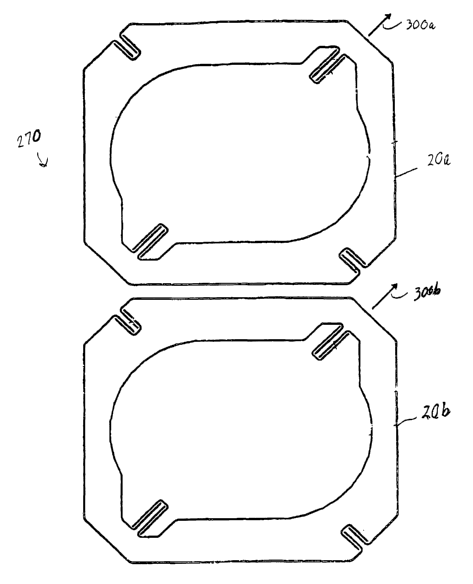
Referring to FIG. 24A, in the mirror strip 270
(only partially shown), when a first mirror 20a is
deflected around its outer axis, the resulting direction
300a of the airflow is close to 45 degrees to the length
of the silicon strip. Hence, the pressure wave tends to
_3?_
CA 02400294 2002-08-15
WO 01/61400 PCT/USO1/05309
dissipate itself towards the side of the strip without
ever interacting strongly with the next neighbor, mirror
20b. Likewise, with the implementation of FIG. 24B,
using elliptically shaped mirrors 20a, 20b rotating about
axes 302a, 302b, respectively, in respective directions
300a, 300b the interaction is even further reduced
because the shape is better aerodynamically. Hence, the
impact of the flow on the adjacent mirror frames 20a, 20b
is substantially less, because the effective interaction
distance between those mirrors is also enlarged.
Referring to FIG. 25, an alternative embodiment
of the micro strip 10 of FIG. 1, is shown as a micro
strip 310, having a substrate 12 coupled to a silicon
strip 314. If material for the substrate 12 is chosen as
aluminum-oxide or any material that does not match the
expansion coefficient of silicon, the length of the
silicon strip 274 is reduced so that the stresses stay
minimal. That is, on contrast to the strip 26 (of FIG.
1), the silicon strip 314 includes several strip sections
316. The sectioning minimizes the longitudinal stresses.
Further, based on the deformation of bimetallic strips,
reducing the length of the strip by four reduces the
overall bending due to thermal mismatch by a factor of
four.
Although the foregoing describes the use of
electrostatic deflection drive, many of the various
techniques and mechanisms described herein are equally
applicable to a micro-mirror structure or arrangement
that uses electromagnetic deflection drive. One such
arrangement is shown in FIGS. 26A-26B.
Referring to FIG. 26A, a strip assembly 320
- 33 -
CA 02400294 2002-08-15
WO 01/61400 PCT/USO1/05309
that uses magnets 321 in conjunction with current loops
322 and 324 is shown. Magnets 321 produce a transverse
magnetic field that is interacted upon by the two coils
322, 324. Referring to FIG. 26B, top silicon portions
326 are formed in grooves 328 in the magnets 321 on top
of a substrate 330, which carries leads for the coils
322, 324. Torsion members 332, 334 coupled to and
supporting mirror plates 336, 338, respectively, interact
with the magnets 321, such interaction causing the
torsion members to rotate about corresponding axes 340,
342, respectively, to position their respective mirror
plates. The torque on the inner mirror plate 336 also
produces a rotation on the outer axis 342 of the inner
mirror plate 336, which may be controlled by an outer
torsion sensor located on or near one the torsion members
334. Since the outer current loop 324 is completely
outside of area of the inner mirror plate 336, the outer
current loop 324 produces no specific rotation on that
plate.
It will be understood that the rotational axes
may be rotated to have the same deflection efficiency if
the incident beam is at an angle relative to the plane of
the mirror. For example, and referring back to FIG. 26A,
the torsion members 332, 334 and corresponding axes 340,
342 are placed at 45 degree angles relative to the x and
y axes in the plane of the mirror plates 334, 38 mirror
to improves deflection efficiency in a balanced manner
when the plane of the mirror in its rest position is at a
45 degree with respect to the incident beam.
Referring to FIG. 27, an optical path scheme
370 in which the separation between mirrors 372, 374 and
-34-
CA 02400294 2002-08-15
WO 01/61400 PCT/USO1/05309
select ones of collimator blocks 376, 377, 378 and 379.
Each mirror block 372, 374 is shaped to have two separate
angled sections or surfaces, 380a, 380b for block 372 and
382a, 382b for block 374. Thus, and by way of example, a
beam 384 received from the collimator block 376 and
hitting the mirror block 372 may be directed to either
surface 382a, 382b of the opposite mirror block 374 by
rays 384' and 384", respectively, for direction towards
their targeted one of the collimator blocks 377 and 378.
Thus, if the beam 384 is intended for the collimator
block 377, it is directed along the path of the ray 384'
to the surface 382a. If, on the other hand, the beam 384
is intended for the collimator block 378, it is directed
along the path of the ray 384" towards the surface 382b.
A folding mirror 386 can also be present in the
arrangement to fold the optical path into a more compact
form, as described in PCT Application Ser. No. 99 21139,
incorporated herein by reference. Thus, the optical path
scheme 370 advantageously provides for reduced
collimator-to-mirror distances.
An alternative embodiment to the arrangement of
electrodes on a conical shaped substrate, an arrangement
of conical shaped electrodes on a substrate, 400, is
shown in FIG. 28. Referring to FIG. 28A, electrodes 401
are constructed to form a raised structure on a flat
substrate 402. Referring to FIG. 28B, the electrodes 401
are plated in steps 404, e.g., circular shaped platforms
(as shown), onto the flat substrate 402. The electrodes
401 are plated in such a manner as to give rise to a form
that is nearly the same as or similar to the form or
shape of the raised portion 30 that is described as part
-35-
CA 02400294 2002-08-15
WO 01/61400 PCT/USO1/05309
of the substrate 16 in FIGS. lA-1B above. Preferably, in
the embodiment illustrated in FIGS. 28A-28B, the
electrodes 401 are made of ceramic.
Other embodiments are within the scope of the
following claims.
What is claimed is:
-36-