Note: Descriptions are shown in the official language in which they were submitted.
CA 02400869 2002-08-20
Multilayer, laminated card with embedded security element
having relief structures
This invention relates to a multilayer card, in particular credit card,
identity card,
bank card or the like, having a security element with diffraction structures,
in particu-
lar holographic relief structures, and to methods for producing the card.
It is commonly known to equip cards, in particular bank, credit or
identification
cards, with security elements in the form of holograms, kinegrams or the like.
The secu-
rity elements have very specific optical effects which are dependent on the
viewing
angle and can be checked visually without aids and whose production requires
consid-
erable technological effort. The presence of such a security element with the
defined
optical effects is evaluated as an authenticity criterion, i.e. the presence
of such a secu-
rity element is taken as an indication of the authenticity of the card.
Security elements having diffraction structures are usually glued on the outer
sur-
face of the cards. If this is done by the so-called hot stamping technique, as
described
in German laid-open print 33 08 831, these security elements cannot be removed
from
the card without destruction after being glued on the card. Transfer of an
authentic se-
curity element from an e.g. expired card to a counterfeit new card can thus be
ex-
cluded. However, it.is disadvantageous that these elements, precisely because
they
have no inherent stability, are extremely thin and thus mechanically very
sensitive.
Such elements usually wear out relatively fast during use of the card, i.e.
abrasion de-
stroys the layer structure so that the specific optical effect resulting from
the diffrac-
tion structures is lost. Although the security value of holograms, kinegrams,
etc., for
cards is rated relatively high, such security elements are thus not very
suitable for
cards with a given long duration, such as personal identification cards,
passports,
driver's licenses, etc.
There have been various attempts to embed security elements with diffraction
structures in the inside of the card in order to avoid mechanical wear.
However, it has
turned out that customary holograms, kinegrams, etc., are either completely
destroyed
by the action of heat and pressure during the laminating process, or so
greatly impaired
CA 02400869 2008-04-09
-2-
in quality that further use is impossible. There are proposals to handle the
card areas where
the diffraction structures arc embedded more gently during the laminating
process than the
areas having no diffraction structures. According to the proposals, these
areas are exposed to
less high temperatures and possibly also lower laminating pressure during
production.
However, such measures, as described e.g. in EP 0 013 557, could hardly reduce
the degree
of damage to the security elements. Instead, the less stressed card areas have
a poorer film
bond, which is visually recognizable and which tends to lead to splitting of
the card layers in
these areas as a result of bending stresses.
The problem of the invention is therefore to propose multilayer, laminated
cards with
embedded relief structures that can be produced inexpensively and by
conventional
laminating methods and that better withstand the stresses in customary use of
the card.
Accordingly, materials with significantly different softening temperatures are
selected for the layer having the relief structure, on the one hand, and the
card layers to be
laminated, on the other hand.
Since the relief structure of the security element is present in a material
(plastic or
lacquer) that either has a comparatively high softening temperature by nature
or is at least
brought into a state with a high softening temperature after production of the
relief structure,
and since the films from which the card is laminated have a lower softening
temperature
relative thereto, it is ensured that the relief structure of the security
element embedded
between the films of the card is not, or at least not appreciably, affected by
the temperatures
and pressures occurring in the laminating process. The materials for the card
films and for
the relief structure must be selected so that the associated softening
temperatures are at a
sufficiently different level during lamination. Materials used for the films
of the laminated
card are thermoplastics, which have a low softening temperature by nature.
Materials used
for the relief structure can be plastics, lacquers or the like with a higher
softening
temperature, in particular thermosetting
CA 02400869 2002-08-20
-3-
particular thermosetting plastics or cured lacquers or the like. In particular
the
crosslinked materials, such as cured lacquers, are especially suitable for the
inventive
use.
When using cover films of polycarbonate (PC), polyester (PET-A: amorphous
polyethylene terephthalate) or polyvinyl chloride (PVC), especially suitable
materials
for the security element have proved to be crosslinked reaction lacquers or
crystalline
polyester.
Suitable crosslinked reaction lacquers are in particular radiation-curable
lacquers
(referred to in the following as "reaction lacquers"). Especially suitable
ones have
proved to be radically and cationically curing, in particular UV-radiation-
curing, lac-
quers and blue-light-curing lacquers.
Fine relief structures can be incorporated into the aforementioned relief
materials
cost-effectively by embossing either into the thermoplastics or into the not
yet
crosslinked or only partly precrosslinked thermosetting plastics and lacquers.
There are diverse possibilities for incorporating the security element with
the re-
lief structures into the card to be laminated.
For example, the relief structure can be cold- or hot-embossed into a
thermoplas-
tic or not yet finally. crosslinked thermosetting plastic layer. The thus
embossed plastic
layer is transferred or glued to a card film with or without a vacuum
metalization.
On the other hand, the relief structure can be embossed into a not yet
crosslinked
lacquer layer that is present on a transfer film or support layer. Said
lacquer layer, after
curing, is transferred to a film of the card to be laminated for example by
the hot
stamping method with or without a transfer film and with or without a metal
layer va-
por-deposited on the relief structure.
It is also possible for the transfer band or support layer for the
crosslinkable lac-
quer to be formed by a film of the card to be laminated itself. In this case
the lacquer
CA 02400869 2008-04-09
-4-
lacquer layer containing the diffraction structure is integrated in the card
structure together
with the support or transfer layer.
The aforementioned methods for embossing the relief into a lacquer layer and
transferring the lacquer layer to a substrate including the previously
mentioned special
reaction lacquers are extensively described in EP 0 684908 B 1. However, EP 0
684 908 B 1
relates to the application of hologram structures to the surface of in
particular paper
substrates, such as bank notes. It has now surprisingly turned out that the
methods and
lacquers described therein are also applicable in corresponding fashion for
the present
purposes of producing multilayer cards with embedded hologram structures.
Tests have shown that the above-described combinations of materials make it
possible to embed the security elements by conventional laminating methods.
Due to the
higher softening temperature of the plastic materials used for the security
elements, in
particular the microrelief thereof remains largely undamaged.
If the films used for the card structure show a stronger tendency to "flow"
during the
laminating process, however, it can happen that the security elements, if they
are being used
as very thin lacquer layers with a thickness smaller than 5 microns, have
mierotears after the
laminating process that can still disturb the general impression. In these
cases it is
recommendable to embed the security elements together with a support film. As
long as the
security element together with the support film has a thickness of at least 10
microns, these
effects (microtears) normally do not occur. As long as the security element
including the
support layer does not essentially exceed a thickness of about 30 microns, it
can be
integrated into the usual card structure without further additional measures.
If, for whatever
reasons, the security element is designed clearly thicker, e.g. with a
thickness of 100 microns
or more including the support layer, the place where the security element is
to be added to
the card structure must be taken into account by corresponding gaps,
depressions, windows
or the like. Such measures are unnecessary, however, if the support layer is
provided as a
whole-area film of the card structure according to a preferred embodiment. In
this ease, the
sup-
CA 02400869 2002-08-20
-5-
support layer can also be designed clearly thicker than 100 microns. The layer
having
the diffraction structures, by contrast, should not exceed a thickness of 10
microns if it
is provided only in partial areas of the support layer.
In a further preferred embodiment, support layer and diffraction structure
layer
are provided over the whole area, whereby either only the areas where the
optical dif-
fraction effects are required are provided with the reflective metal layer, or
the areas
where no diffraction structures are to be present are overprinted or covered
with
opaque ink.
It is clear to the expert that a good bond between security element and the
adjoin-
ing layers of the card structure is necessary for attaining a uniform optical
general im-
pression. This is obtained by carefully coordinating the individual layers
with each
other. If films, lacquers or printing inks are to be combined that bond poorly
with each
other in the laminating compound, additional adhesive layers that bond well
with both
materials should be provided between these layers. Such adhesives are known to
the ex-
pert.
If a whole-area support layer is used, it can also be used as an inlay layer
that
bears the double-sided printed image of the card. If the support layer is of
transparent
design, one can homogeneously print partial areas, on the one hand, and leave
partial
areas free, on the other hand, to achieve the optical appearance of a usual
card wherein
a transparent window is provided in which a security element with optical
diffraction
structures can be recognized. If the security element has a metallic
reflecting layer, it
can be viewed from both sides but it is not possible to see through the
"window" of the
card. If such effects are desired, the metallic reflecting layer can be
completely or
partly left out. If only interruptions in the form of characters, patterns or
the like are
provided in the metal layer, an additional security effect is obtained since
these inter-
ruptions can be checked in transmitted light, whereas the diffraction effects
overlaying
the total window are to be checked at the defined viewing angles.
If a consistently opaque support layer is used, diffraction structures can be
pro-
vided on both sides of the support layer optionally in the same area of the
card, which
can then likewise be checked from both sides. In this case, the optical
diffraction ef-
CA 02400869 2008-04-09
-6-
diffraction effects on both sides can also have different diffraction effects,
e.g. different
holographic information.
If a whole-area diffraction structure layer is provided on the transparent
support layer
and overprinted with differently disposed window areas from both sides, the
diffraction
structure is visible in special areas only from one side and in other areas
only from the other
side. In cases where window areas are provided on both sides, the diffraction
structure is
recognizable at the same place from both sides.
The use of a whole-area support layer has very special advantages since it can
be
processed just like every other layer of the card structure. Regardless of
whether the
diffraction structures are provided on the whole or on part of the area, they
can be glued on
and embossed in placed fashion in the known way as film sheets or as rolls.
The invention thus provides according to an aspect, for a card including a
plurality of
laminated layers between which a security element with a relief structure is
embedded. The
card is characterized in that the relief structure is present in a plastic or
lacquer layer of the
security element that has a higher softening temperature than the laminated
layers of the card
between which the security element is embedded.
According to another aspect, the invention provides for a method for producing
a
multilayer laminated card, including a plurality of laminated layers between
which a security
element with a relief structure is embedded. The method comprises the steps
of: providing a
reaction lacquer layer on a support layer; embossing a relief structure into
the reaction
lacquer layer and activating the crosslinking of the reaction lacquer layer to
produce a stable
relief layer; applying an adhesive layer to the relief layer, optional l y
after at least partial
metalization and covering thereof with a protective lacquer layer; contacting
the adhesive
layer with a first layer of the card to be laminated; and laminating the first
layer with at least
one further layer of the card so that the relief layer and protective lacquer
layer are embedded
between the first and further layers of the card, the laminating temperature
being below the
softening temperature of the relief layer.
CA 02400869 2008-04-09
-6a-
According to yet another aspect, the invention provides for a method for
producing a
multilayer laminated card, including a plurality of laminated layers between
which a security
element with a relief structure is embedded. The method comprises the steps
of: providing a
reaction lacquer layer on a first layer of the card to be laminated; embossing
a relief structure
into the reaction lacquer layer, and activating the crosslinking of the
reaction lacquer to
produce a stable relief layer; applying an adhesive layer to the relief layer,
optionally after at
least partial metalization of the relief surface and covering thereof with a
protective lacquer
layer; and contacting the adhesive layer with a further layer of the card to
be laminated, and
laminating the first and further layers of the card so that the relief layer
is embedded between
the first and further layers, the laminating temperature being below the
softening temperature
of the relief layer.
According to a further aspect, the invention provides for a method for
producing a
multilayer laminated card, including a plurality of laminated layers between
which a security
element with a relief structure is embedded. The method comprises the steps
of: providing a
plastic film; embossing relief structures into the plastic film on both sides;
applying an
adhesive layer to the relief structures, optionally after at least partial
metalization of the relief
surface and covering thereof with protective lacquer layers; contacting the
adhesive layer
with a first layer of the card to be laminated; and laminating the first layer
with at least one
further layer of the card so that the relief layer is embedded between the
first and further
layers, the laminating temperature being below the softening temperature of
the relief layer.
Further advantages and embodiments will be explained with reference to the
figures.
It is pointed out that the figures do not offer a true-to-scale representation
of the invention
but are only for illustration. The term "security element" used in the
following text includes
the lacquer or plastic layer into which the relief is embossed and, if
present, the metal layer
vapor-deposited on the relief, the protective layer, the transfer or support
layer (if it is
embedded in the card as well) and the adhesive layers connecting the security
element with
the adjoining layers of the multilayer card. Diffraction structures include
all structures
having optical diffraction effects, in particular holograms, kinegrams,
moviegrams,
pixelgrams, etc.
CA 02400869 2008-04-09
-6b-
Fig. 1 shows an inventive multilayer, laminated card with an embedded security
element in a plan view,
Figs. 2-5 show sections through different cards with laminated-in security
elements,
Fig. 6 shows a variant of the security element according to Fig. 2, here with
a support
layer,
Fig. 7 shows a variant of the security element according to Fig. 2 wherein the
security
element has been produced directly on a card film,
CA 02400869 2002-08-20
-7-
Fig. 8 shows a variant of the security element according to Fig. 2 with two op-
posing relief structures, and
Fig. 9 shows a variant of the security element according to Fig. 6 with a
support
layer and likewise two opposing relief structures.
Fig. 1 shows a plan view of multilayer laminated card 1, for example a credit
card, in which security element 2 with relief structures, in particular a
hologram, is
embedded. Additionally, the card has a double-sided printed image and
optionally fur-
ther elements and security structures such as a chip, signature stripe and the
like,
which are not shown in Fig. 1. Depending on the requirements, security element
2 can
have the form of a thread or band or be designed as a label-like element
(patch) with
defined outline forms.
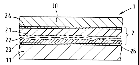
Fig. 2 shows a cross section through card 1 in the area of security element 2
ac-
cording to a first embodiment of the invention. One can see card cover layers
10 and
11 with security element 2 embedded therebetween. Security element 2 comprises
transparent relief layer 21 into which the relief forming the holographic
diffraction
structures is embossed, vapor-deposited metal layer 22 (optional) that
enhances the
optical effect of the diffraction structures, transparent protective lacquer
layer 26 and
the two likewise transparent adhesive layers 23 and 24 firmly connecting
security ele-
ment 2 with cover layers 10 and 11.
Cover layers 10 and 11 are transparent or at least have transparent window
areas
in the area of security element 2 so that the hologram is recognizable from
both sides
of the card. The holographic information is then recognizable mirror-inverted
from the
back, and visual three-dimensional effects are also inverse to each other
depending on
the manner of viewing.
Fig. 2 shows the simplest possible structure of a multilayer laminated card,
in-
cluding only two cover layers 10, 11. Further layers can be provided, in
particular a usu-
ally opaque core layer. If an opaque core layer is provided as an additional
layer, the
hologram is only to be seen from one side, unless the opaque inlay has a
transparent
window area where the hologram is disposed.
CA 02400869 2002-08-20
-cg-
Metal layer 22 vapor-deposited on relief layer 21 enhances the optical effect
of
the diffraction structures. It can also be provided only in a partial area; in
particular it
can have interruptions in the form of characters, patterns, images, logos or
the like.
Security element 2 can also be overprinted with a printed image so that the
holo-
gram is visible only in the gaps of the printed image. The printed image can
be exe-
cuted with any desired inks. If inks are used that change color likewise in
accordance
with the viewing angle (e.g. inks with liquid crystal polymer pigments,
iriodines or
other viewing-angle-dependent inks), this effect can supplement the viewing-
angle-
dependent optical effect of the hologram.
As mentioned at the outset, the choice of material is of particular importance
for
the purposes of the present invention, in particular the choice of material
for relief
layer 21, since this layer must be sufficiently temperature- and pressure-
resistant so as
not to lose the relief structure in the laminating process. Cover layers 10,
11 have a
low softening temperature compared to relief layer 21. Relief layer 21
consists of a
plastic with an accordingly higher softening temperature, in particular of
crosslinked,
i.e. cured, duromer, or a crosslinked lacquer. The lacquers or lacquer systems
are
known from EP 0 684 908 Bl.
Security element 2 shown in Fig. 2 has first lacquer layer 21 in which the
diffrac-
tion structures are embossed, and metal layer 22, protective lacquer layer 26
and adhe-
sive layers 23, 24. Relief layer 21 can be a plastic film into which the
relief was em-
bossed and which was then punched out, optionally after being metalized and
coated
with protective lacquer layer 26 and adhesive layers 23, to be embedded in the
layer
structure of card 1. Adhesive layer 24 is provided on cover film 10. Relief
layer 21 can
also be a crosslinked, in particular radiation-cured, lacquer which is
initially present on
a transfer film in the uncrosslinked or partly precrosslinked state and into
which a re-
lief structure is embossed, to be transferred to cover layer 11 without the
transfer film
by the hot stamping method after the lacquer cures. The transfer films with
security
elements 2 are embossed on endless webs for this purpose, so that security
elements 2
can be applied to cover film 11 and then laminated with further cover film 10
in a con-
CA 02400869 2002-08-20
-9-
cover film 10 in a continuous process involving detachment of the transfer
film. This
;netllod is extensively described in EP 0 684 908 B 1.
In the card structure shown in Fig. 2, security element 2 has a layer
thickness of
about 2 to 5 microns. The overall card structure has a thickness of 760 to 800
microns
in the welded state of the single layers.
In Fig. 3 the card structure described in Fig. 2 is modified to the effect
that two
further films 27, 28 are provided besides security element 2 and cover films
10 and 11.
Said internal card layers 27, 28 enclose security element 2. This card
structure has the
advantage that layers 27 and 28, being internal card layers, can be handled
separately
from the cover films. These layers usually have the printed image, whereby one
of the
two layers can also be of opaque design so that the card inlay is not
transparent, as is
commonly known.
In the card structure shown in Fig. 3, security element 2 is applied directly
to film
layer 27 since lacquer layer 21 was applied over the whole area or partially,
the relief
structure embossed thereinto, as described above, the lacquer cured, metal
layer 22
vapor-deposited and finally the relief structure covered with further lacquer
layer 26.
To permit an intimate bond of the security element area with film 28 in the
later lami-
nating process, adhesive layer 23 can be additionally provided on lacquer
layer 26. If
the materials of lacquer layer 26 and film 28 permit an intimate bond in the
laminating
process, adhesive layer 23 can also be omitted.
In Fig. 4 the card structure stated in Fig. 3 is modified to the effect that
security
element 2 was not produced directly on film 27 but is produced as a separate
element
that is transferred to film 27 by the transfer method. For this reason it can
be expedient
to provide adhesive layers 23 and 24 on both sides of the security element for
the
transfer process, on the one hand, and for the laminating process, on the
other hand.
Fig. 5 shows a further variant of the card structure wherein security element
2 is
applied to the side of the inlay consisting of films 27, 28 that faces a cover
film. In this
case, both films 27 and 28 can be of opaque design. Security element 2 can be
pro-
duced both on the film itself (see Fig. 3) or be transferred as a prepared
transfer ele-
CA 02400869 2002-08-20
-10-
element to the surface of film 27 (see Fig. 4). In the present case, the
security element
is designed as a transfer element and fixed on film 27 with adhesive layer 24.
In Figs. 3, 4 and 5 the card inlay has two films 27 and 28. This has the
advantage
that the card, whose overall thickness is standardized, consists of single
layers having
a thickness that can be processed easily. It is also possible to provide
further layers in
the card structure, thereby permitting the thickness of the single layers to
be reduced
further. This seems expedient in particular when a relatively thick security
element of
for example 100 microns or more is to be used and a gap is to be provided
therefor in
the card structure. In this case, the film in which the gap is incorporated
should have
roughly the thickness of security element 2. Although the inventive card
structure
makes it basically possible to integrate the security element into the card
structure and
process it in the laminating process without any further precautions, it is
still expedient
not to embed security elements of any thickness into the layer structure
during the
laminating process. Practice has shown that the film material, even in the
heated state,
cannot be displaced or compressed in any quantity for embedding additional
elements.
Even if it was possible (e.g. by increasing laminating pressure and laminating
tempera-
ture), the "flowing away" of the film material would cause a change, i.e.
distortion, of
the printed image, thereby reducing the card quality as a whole. By providing
a gap
this can be avoided since the laminating process must then only effect the
intimate
bond of the card layers and no, or little, compression or displacement of film
material
is necessary.
Fig. 6 shows a further embodiment of the invention wherein security element 2
includes layer 21 with a relief structure in a crosslinked lacquer and support
layer 25
for the crosslinked lacquer. Otherwise the structure of card 1 corresponds to
the struc-
ture described in Fig. 2. In the present case, security element 2 consists
substantially of
lacquer layer 21 (with relief structure), metal layer 22, protective lacquer
layer 26 and
support layer 25. The incorporation of security element 2 between cover films
10, 11
can be effected similarly to the incorporation of security element 2 described
with ref-
erence to Fig. 2 when security element 2 is embedded as a label-like element
(patch).
In a preferred embodiment, however, support layer 25 has the format of the
card, i.e.
the support layer is integrated in the card over the whole area. Layers 21,
22, 26 are
CA 02400869 2002-08-20
-11-
21, 22, 26 are directly connected with support layer 25. The thickness of
layers 21, 22,
26 is smaller than 10 microns, preferably about 2 to 5 microns, the overall
thickness of
security element 2 (with support layer 25) is about 30 microns.
The layer structure of card 1 is to be selected, as mentioned above, so that
the in-
dividual layers are interconnected preferably homogeneously at the laminating
tem-
perature coordinated with the layer structure, the associated laminating
pressure and
the defined laminating time, but without destroying the microrelief of the
hologram.
This goal can be reached according to the invention by the combination of very
different materials as long as it is ensured that the layers of the card
structure become
sufficiently "soft" during the laminating process to bond well in the boundary
layers
but the layer bearing the relief remains so stable that the microrelief is not
deformed or
reversed.
The following table compiles the softening temperatures of some film materials
(PET: polyethylene terephthalate; ABS: acrylonitrile-butadiene-styrene):
Film material Softening temperature [ C]
PC 146 -148
Thermoplastic polyester 74 - 76
PVC 65 - 80
ABS 90
Crystalline PET > 200
The lacquer used for layers 21, 26 has a softening temperature greater than
240 C. It is thus clearly more temperature-stable than the film materials
stated in the
table.
The further table now states some combinations of materials, together with the
laminating temperature of the laminating plant, that can be used for producing
cards
with embedded security elements.
CA 02400869 2002-08-20
-12-
Cover film / Inlay Support film Laminating temperature
Polycarbonate Crystalline PET about 175 C
Thermoplastic polyester PC or cryst. PET about 130 C
PVC PC or cryst. PET about 150 C
ABS PC or cryst. PET about 140 C
Fig. 7 shows a further embodiment of the present invention wherein relief
layer
21 is again present as a crosslinked lacquer. In this case, relief layer 21
was not pro-
duced on a transfer band, cured and then transferred, but relief layer 21 was
produced
directly on cover layer 10. That is, cover layer 10 forrned the carrier or
support layer
for lacquer layer 21 during embossing of the relief structure into the not yet
cross-
linked lacquer layer. In this production variant, security element 2 can be
produced on
cover layer 10, provided with metal layer 22 and covered with protective
lacquer layer
26. When metal layer 22 is provided, protective layer 26 preferably consists
of the
same reaction lacquer as relief layer 21.
If metal layer 22 is omitted in the present example or the other embodiments,
protective lacquer layer 26 must consist of a different lacquer from that used
for layer
21. This lacquer must have a refractive index preferably differing from relief
layer 21
so that the optical diffraction effects are still perceptible. This different
lacquer should
likewise have a higher softening temperature than the cover or inlay films.
The continuous method for applying security element 2 to a substrate, here
cover
layer 10, is likewise described in EP 0 684 908 B l, the relevant disclosure
of which is
incorporated herein by reference.
Figs. 8 and 9 show two further embodiments of the invention wherein security
element 2 is equipped with relief structures and optionally metallic coatings
22a, 22b
and protective lacquer layers 26a, 26b on opposing sides. Cover layers 10, 11
and ad-
joining adhesive layers 23, 24 are therefore to be of transparent design at
least in the
area of the relief structures. In the embodiment of Fig. 8, relief layer 21
consists of a
plastic material with a comparatively high softening temperature, preferably
of crystal-
CA 02400869 2002-08-20
-13- crystalline polyester or polycarbonate (PC). Security element 2 has a
thickness of 30
microns for example.
Security element 2 according to the embodiment of Fig. 9 instead includes cen-
tral support layer 25 with a thickness of about 90 microns on both sides of
which lac-
quer layers 21 a, 2 lb with relief structures, metal layers 22a, 22b and
protective lacquer
layers 26a, 26b are applied.
The securi ty element has a thickness of about 100 microns. While a one-sided
re-
lief structure is usually produced by means of one embossing cylinder, the
opposing
relief structures according to Figs. 8 and 9 can be produced for example
simultane-
ously by guiding the material to be embossed through the gap of two opposing
em-
bossing cylinders. Both reliefs are then provided with the metal layers and
covered
with the protective lacquer layers.
Numerous other embodiments are possible for realizing the inventive solution.
The inventive solution makes it possible for the first time to laminate
security elements
with relief structures, in particular holographic diffraction structures, into
a multilayer
card without appreciably impairing the relief structures during lamination of
the card.
The selected materials with different softening temperatures permit the
security ele-
ment to remain inherently stable at the laminating temperatures that occur so
that it
requires no additional protection during the laminating process. Especially
good re-
sults have been achieved with the stated materials and combinations of
materials. The
security element embedded in the multilayer card is not exposed to direct
mechanical
stress and thus not subject to direct wear in later use, so that the life of
the security
element corresponds to the life of the card. .