Note: Descriptions are shown in the official language in which they were submitted.
CA 02401459 2002-08-28
WO 01/66997 PCT/USO1/07247
LIGHTING APPARATUS HAVING QUANTUM DOT LAYER
Field of the Invention
The present invention relates to fluorescence, and more specifically, to
structures comprising material that
fluoresces when exposed to light.
Background of the Invention
Organic fluorescent dyes have been employed in structures comprising a plate
of a material that is
transparent to light. The material has an organic fluorescent dye distributed
within its volume. The plate has a top
surface and is surrounded by edges. The top surface of the transparent plate
is oriented to receive the light. Light
incident on this top surface penetrates into the plate and is absorbed by the
organic fluorescent dye which in turn
emits longer wavelength light having a narrow wavelength distribution. The
light emitted by the fluorescent dye
propagates through the plate to its edges. The plate is preferably thin so as
to provide a large surface area for
collecting light and has narrow edges where the light emitted from the
fluorescent dye exits the plate. Large amounts
of light can therefore be collected and concentrated into a smaller region.
One disadvantage of such organic-based
structures is that they have a short lifetime, lasting typically about 1-4
years. The organic fluorescent dyes contained
within the structure decompose upon extended exposure to ultraviolet (UV)
light, which, for instance, is abundant in
sunlight. Thus, there is a need for a structure for collecting light and
converting it into high intensity narrow band
illumination that is not rendered inoperative by UV light.
Summary of the Invention
In one aspect of the invention, an apparatus comprises a layer of quantum dots
that emits light in response
to exposure to pump radiation and a waveguide which receives and guides light
emitted by the layer of quantum dots.
In another aspect of the invention, a waveguide has a substantial number of
quantum dots which emit light in
response to pump radiation. The quantum dots are disposed in relation to the
waveguide such that light emitted by the
quantum dots is captured by the waveguide and guided therein.
2S In yet another aspect of the invention, a method of illumination comprises
illuminating quantum dots disposed
over a relatively large area with pumping radiation. These quantum dots are
used to emit light in response to the
pumping radiation. Light emitted by the quantum dots is collected and used to
illuminate a relatively small surface
area.
Brief Description of the Drawings
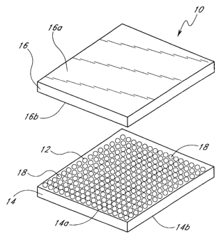
FIGURE 1 A is a perspective view of a fluorescent structure of one embodiment
in the present invention;
FIGURE 1B shows an exploded view of the fluorescent structure depicted in
FIGURE 1A;
FIGURE 2 is a cross-section of the fluorescent structure shown in FIGURES 1 A-
1 B;
FIGURE 3 is a schematic drawing of a single quantum dot that is contained in
the fluorescent structure of
FIGURES 1A-1B and 2;
-1-
CA 02401459 2002-08-28
WO 01/66997 PCT/USO1/07247
FIGURE 4 is a cross-section of the fluorescent structure shown in FIGURES 1A-
1B depicting the path of
several rays of light emitted by a quantum dot;
FIGURE 5 is a perspective view of a fluorescent structure that includes a non-
imaging optical element
mounted on an edge of the structure; and
FIGURE 6 is a fluorescent structure in accordance with the present invention
comprising photovoltaic cells
mounted on edges of the structure.
Detailed Description of the Preferred Embodiment
As depicted in FIGURES 1A-1B and 2, a fluorescent structure 10 comprises a
layer of quantum dots 12
sandwiched between a base layer 14 and a protective layer 16. The dots emit
light at a particular wavelength in
response to exposure to 'light, particularly sunlight. The base layer 14 has a
top and a bottom surface 14a, 14b as
well as edges 14c. The bottom surface 14b of the base layer 14 forms the
bottom of the fluorescent structure 10.
The protective layer 16 also has a top and a bottom surface 16a, 16b as well
as edges 16c. The top surface 16a
forms the top surface of the fluorescent structure 10. In the embodiment
shown, the protective layer 16, and the base
layer 14 are both transmissive to light of the emission wavelength of the
quantum dots. Each layer 14, 16 has an
index of refraction, n, greater than unity at that wavelength (e.g.,
approximately 1.5). The base layer 14 and the
protective layer 16 may be rigid, but are preferably formed of thin, flexible
film so that the fluorescent structure 10
can readily be applied to a curved or irregular surface or bent into a desired
shape. The base layer 14 and the
protective layer 16 may comprise, for example, a polymeric material such as
plastic or silicone. The base layer 14 is
sufficiently thick to support the layer of quantum dots 12 when the protective
layer 16 is in place. The layer of
quantum dots 12 comprises an array of individual quantum dots 18 spread across
the top surface 14a of the base
layer 14. Preferably, the quantum dots 18 are uniformly distributed over this
top surface 14a in a layer sufficiently
thick so as to absorb pump radiation incident thereon. The quantum dots
themselves are preferably between about 2
to 10 nanometers (nm) in size. In the preferred embodiment, the structure 10,
which includes the base layer 14, the
layer of quantum dots 12, and the protective layer 16, is preferably about 500
to 1000 micrometers (gym) thick. The
length and width of the fluorescent structure 10, however, is significantly
larger, for example, the length or width may
be about'h inch (in.) to ten or more feet (ft.).
Quantum dots 18 such as in the layer of quantum dots 12 are well known in the
art and are available from
numerous sources. One kind of quantum dots, for example, is sold under the
tradename Qdot° and is manufactured
and distributed by Quantum Dot Corp. of Palo Alto, California.
As depicted in FIGURE 3, a single quantum dot 18 comprises a small group of
atoms 20 that form an
individual particle 22. These quantum dots 18 may comprise various materials
including semiconductors such as zinc
selenide (ZnSe), cadmium selenide (Gdse), cadmium sulfide (CdS), indium
arsenide (InAs), and indium phosphide (InP).
Another material that may suitably be employed is titanium dioxide (TiOz). The
size of the particle 22, i.e., the
quantum dot 18, may range from about 2 to 10 nm. Since the size of these
particles 22 is so small, quantum physics
-2-
CA 02401459 2002-08-28
WO 01/66997 PCT/USO1/07247
governs many of the electrical and optical properties of the quantum dot 18.
One such result of the application of
quantum mechanics to the quantum dot 18 is that quantum dots absorb a broad
spectrum of optical wavelengths and
re-emit radiation having a wavelength that is longer than the wavelength of
the absorbed light. The wavelength of the
emitted light is governed by the size of the quantum dot 18. For example, CdSe
quantum dots 5.0 nm in diameter emit
radiation having a narrow spectral distribution centered about 625 nm while
quantum dots 18 comprising CdSe 2.2 nm
in size emit light having a center wavelength of about 500 nm. Semiconductor
quantum dots comprising CdSe, InP,
and InAs, can emit radiation having center wavelengths in the range between
400 nm to about 1.5 Vim. Titanium
dioxide TiOz also emits in this range. The linewidth of the emission, i.e.,
full-width half-maximum (FWHM), for these
semiconductor materials may range from about 20 to 30 nm. To produce this
narrowband emission, quantum dots 18
simply need to absorb light having wavelengths shorter than the wavelength of
the light emitted by the dots. For
example, for 5.0 nm diameter CdSa quantum dots light having wavelengths
shorter than about 625 nm is absorbed to
produce emission at about 625 nm while for 2.2 nm quantum dots comprising CdSe
light having wavelengths smaller
than about 500 nm is absorbed and re-emitted at about 500 nm. In practice,
however, the excitation or pump radiation
is at least about 50 nanometers shorter than the emitted radiation. These and
other properties of quantum dots are
well known and are described in by David Rotman in "Quantum Dot Com,"
Technoloey Review, JanuarylFebruary
2000, pp. 50-57.
To construct the fluorescent structure 10 depicted in FIGURES 1 A-1 B and 2,
the layer of quantum dots 12 is
deposited on the top surface 14a of the base layer 14 and the protective layer
16 is formed over the exposed layer of
quantum dots. The protective layer 16, which seals the layer of quantum dots
12 against the base layer 14, acts to
protect the quantum dots 18 that may otherwise be exposed to the outside
environment from damage. The layer of
quantum dots 12 may be deposited on the top surface 14a of the base layer 14
by evaporation of a liquid carrier in
which the quantum dots are dispersed or by providing a polymer matrix in which
the quantum dots are contained on the
surface. Alternatively, quantum dots 12 that can withstand high temperatures
employed in injection molding can be
mixed in a polymeric solution which is injection molded to form a layer of
fluorescent material comprising quantum dots
suspended in plastic. By employing these and other techniques, roils of the
fluorescent structure 10 hundreds of feet
long could be produced for industrial and commercial use.
The fluorescent structure 10 itself may be mounted against a surface where
light can be received by the top
or bottom surface 16a, 14b of the fluorescent structure. Since the fluorescent
structure 10 is flexible, it will conform
to the contours of a curved surface, especially in the case where the
fluorescent structure has a thickness less than
500 ~,m. The fluorescent structure 10 may also be sandwiched between two
plates, wherein at least one of the
plates is optically transmissive to some light absorbed by the quantum dots
18. These plate may comprise a plastic or
polymeric substance such as acrylic material. Preferably, a small air gap
separates each plate from the fluorescent
structure 10 such that light is confined therein. Alternatively, the plates
may have a lower refractive index than that
of the protective layer 16 and the base 14 so as to ensure confinement of the
light within the protective layer andlor
base. If the fluorescent structure 10 is to be mounted in a manner where the
base layer 14 or the protective layer 16
-3-
CA 02401459 2002-08-28
WO 01/66997 PCT/USO1/07247
is supported against a surface having a higher refractive index, a cladding
layer, i.e., a layer of material having a lower
refractive index, needs to be introduced at this location to prevent the base
layer or protective layer from contacting
the material having a higher refractive index to ensure confinement.
In other embodiments, an optically transmissive plate, comprising for example
polymeric material having a
refractive index of approximately 1.5 can be abutted against the base layer 14
andlor the protective layer 16. In this
configuration, the transmissive plate will act as a waveguide as long as the
base andlor protective layer 14, 16 has of
a similar index of refraction. Light from the fluorescent structure 10 will be
coupled into the plate and guided
therethrough to its edges. This plate need only have a higher refractive index
than its ambient medium which might be
air andlor rests on or is in contact with material having a lower refractive
index. In addition, this plate is preferably
optically transmissive to the light emitfied by the quantum dots 18.
Preferably, this plate also transmits light having
suitable wavelength for pumping the quantum dots 18. This plate may comprise,
for example, acrylic material. In one
embodiment, two such plates are employed, one adjacent the base layer 14, and
one adjacent the protective layer 16.
As depicted in FIGURE 4, light, such as sunlight, incident on the fluorescent
structure 10 provides pump
radiation represented by arrows 24. Such pump radiation is transmitted through
the protective layer 16 to the layer of
quantum dots 12. The quantum dots 18 will absorb a portion of the pump
radiation, namely the light having
wavelengths within its absorption band, and will produce optical emission
having wavelengths corresponding to its
emission band. Upon excitation by the pump radiation, the quantum dots 18 will
radiate in different directions as
indicated by arrows 26. Some of the optical emission radiated by the quantum
dots 18 will be directed into the
protective layer 16, some into the base layer 14, and some into the layer of
quantum dots 12. Optical emission
incident on other quantum dots 18 is likely to be absorbed by these other dots
while light directed into the protective
layer 16 or the base layer 14 will either escape through the top or bottom
surfaces 16a, 14b respectively, or will
propagate within the layers toward the edges 16c, 14c where the light can
escape the fluorescent structure 10.
More specifically, optical emission from a quantum dot 18 (represented by a
ray 28 shown in FIGURE 4) that
enters the protective layer 16 and is incident on the top surface 16a thereof
at an angle measured with respect to the
normal to the top surface that is larger than the critical angle will be
totally internally reflected from the top surface
toward the bottom surface 16b of the protective layer where it is again
totally internally reflected if the light incident
with respect to the normal to the bofitom surface is at an angle larger than
the critical angle. As a result of being
totally internally reflected at the top and bottom surfaces 16a, 16b of the
protective layer 16, light emitted from
quantum dots 18 is trapped in this layer and guided toward the edges 16c of
the fluorescent structure 10. Essentially,
the protective layer 16 acts as a waveguide channeling optical emission from
the quantum dots 18 toward the edges
16c of the fluorescent structure 10. Optical emission entering the base layer
14 is also guided in a similar manner
toward the edges 14c. Light not trapped in the layers 14, 16 will either be
absorbed in the quantum dots 18 or will
exit the fluorescent structure 10 at the top or bottom surfaces 16a, 14b.
Preferably, however, greater than half of the
light radiated by the quantum dots 18 will be coupled into the protective and
base layers 16, 14 where it will be guided
to the edges 16c, 14c. Optical omission that is incident on the edges 14c, 16c
at an angle measured with respect to
-4-
CA 02401459 2002-08-28
WO 01/66997 PCT/USO1/07247
the normal to the edges that is smaller than the critical angle will not be
reflected, but rather will exit such edges.
Although FIGURE 4 depicts pump radiation as incident on the top 16a of the
fluorescent structure 10, it will be
understood that, where the base layer 14 is also substantially transparent,
pump radiation incident on the bottom 14b
of the fluorescent structure may similarly pump quantum dots 12 to re-radiate
light.
The structure and composition of the base layer 14 and the protective layer 16
as well as the layer of
quantum dots 12 should preferably facilitate the collection of pump radiation
and the transport of light emitted from
the quantum dots 18 to the edges 14c, 16c of the fluorescent structure 10. For
example, the protective layer 16 and
possibly the base layer 14 are preferably optically transparent to the pump
illumination to allow this light to reach the
layer of quantum dots 12. Also, the protective layer 16 and the base layer 14
are preferably optically transparent to
light emitted by the quantum dots such that this light can be guided through
these layers to the edges 16c, 14c of the
fluorescent structure 10. Additionally, the protective layer 16 and the base
layer 14 each preferably have an index of
refraction, n, that is larger than air such that light emitted by the quantum
dots 18 that enters into the protective layer
and the base layer experiences total internal reflection and is therefore
guided along these two layers to the edge 16c,
14c of a fluorescent structure 10. Furthermore, although the layer of quantum
dots 14 could comprise a plurality of
monolayers, the layer preferably comprises a single monolayer so as to
minimize the occurrence of light emitted by a
quantum dot being absorbed by another quantum dot.
In the case where the spatial extent of the surface 16a, 14b of the
fluorescent structure 10 where the pump
radiation is received is large compared to the light output surfaces 16c, 14c,
a concentrating effect is produced, so
that large amounts of light can be collected and concentrated into a smaller
region. In particular, light collected, for
example, by the top surface 16a of the protective layer 16 having surface area
AT°p IS transmitted to the layer of
quantum dots 12. Resultant optical emission from the quantum dots 18 is
coupled into the protective layer 16a and
radiated out its edges 16c having a surface area, AEOCe- If AT°P > >
AEOGE then intense emission is produced at the
edges 16c, the brightness of optical emission at the edges being larger than
the brightness at a given region on the
layer of quantum dots 12 having surface area equal to AEOSe.
Thus, the fluorescent structure 10 can be employed to create intense color
illumination. Since the quantum
dots 18 emit light having a narrow wavelength distribution, the light exiting
at the edges 16c, 14c of the fluorescent
structure 10 possesses a specific color. This color depends on the type of
quantum dots 18, in particular on the size
of the quantum dots. Accordingly, by employing different types of quantum dots
18, light sources of different colors
can be produced. Furthermore, by stacking a first fluorescent structure 10
that includes a layer of quantum dots 12
emitting light of one color on a second fluorescent structure having a layer
of quantum dots that emit light of another
color, unique colors and(or patterns of colors can be created. The direction
of the colored light emitted from the edges
14c, 16c of the fluorescent structure 10 can also be controlled with an
optical element mounted thereon. As shown in
FIGURE 5, for example, a non-imaging optical element 30 can be affixed to the
edges 14c, 16c of the fluorescent
structure 10 so as to alfier the direction the optical emission exiting the
edges, limiting this emission to a specific range
of angles less than 180°. In addition, highly reflective thin film with
specular reflectivity preferably in excess of 95%
-5-
CA 02401459 2002-08-28
WO 01/66997 PCT/USO1/07247
such as for example, 3M Radiant Mirror Film, Model No. VM2000, available from
3M can be affixed to those edges
from which emission is not desired.
Pump radiation may comprise natural fight, i.e., sunlight, or artificial light
such as from UV or blue light
emitting diodes (LED) or fluorescent lights. The light incident on the
fluorescent structure 10 need only comprise
radiation having wavelengths within the absorption spectrum of the quantum
dots 18 in the layer of quantum dots 12.
Since the absorption spectrum of the quantum dots 18 comprises wavelengths
shorter than the wavelength of
emission from the quantum dots, the pump radiation includes wavelengths
shorter than the emitted wavelengths. For
example, sunlight can be employed to pump a fluorescent structure 10 having a
layer of quantum dots 12 comprising
CdSe particles 5.0 nm in diameter, which emit at an optical wavelength of 625
nm, since the sun radiates light across
a broad spectrum including light having wavelengths at least 50 nm shorter
than 625 nm. Alternatively, such a
fluorescent structure 10 can be pumped with one or more light emitting diodes
(LEDs) that provide light of, for
example, 550 nm. Incandescent lights as well as ultraviolet light sources such
as UV LEDs would also be capable of
exciting the layer of quantum dots 12.
The fluorescent structure 10 described above can be employed in various
applications requiring bright,
narrowband illumination. For example, light sources of colored illumination
are useful in constructing signs, in creating
artistic or architectural designs, and in producing bright regions of color,
including outlines, bands and borders on
products including but not limited to furniture, automobiles, appliances,
electronics, clothes or any other object where
bright color is useful for aesthetic or functional purposes. These fluorescent
structures 10 are advantageously capable
of producing intense colored light illumination during daytime when exposed to
daylight. Thus, sunlight can be
employed to power the fluorescent structure 10 described above. Since, quantum
dots do not degrade with exposure
to UU rays such as produced by the sun, the structure 10 has a long lifetime.
By way of example, the fluorescent
structure 10 can be incorporated in architectural features, such as a border
to highlight a rooftop of a building during
the daytime. Further, as illustrated in FIGURE 6, photovoltaic solar cells 32
can he positioned at the edges 14c, 16c of
the thin fluorescent structure 10 to receive narrow band illumination produced
by the layer of quantum dots 12 upon
exposure to sunlight. The concentrating effect of a fluorescent structure 10
having a large width and length will
enhance the efficiency of generating electricity from sunlight.
Many other applications for the fluorescent structure 10 are considered
possible, the relevant applications
not being limited to those specifically recited above. Also, the present
invention may be embodied in other specific
forms without departing from the essential characteristics as described
herein. The embodiments described above are
to be considered in all respects as illustrative only and not restrictive in
any manner.
-6-