Note: Descriptions are shown in the official language in which they were submitted.
CA 02401767 2002-08-29
WO 01/65629 PCT/USO1/05074
DESCRIPTION
H~i h Temperature Superconductor Tunable Filter
Related Application
This application relates to U.S. Ser. No. 09/268,786, filed March 16, 1999.
Field of the Invention
This invention relates to a high temperature superconductor (HTS) tunable
filter.
More particularly, this invention relates to an HTS filter tunable by
actuating a magnetic
driver.
Background of the Invention
The need for a high-quality factor (Q), low insertion loss tunable filter
pervades a
wide range of microwave and RF applications, in both the military, e.g.,
RADAR,
communications and ELINT, and the commercial fields such as in various
communications applications, including cellular. Placing a sharply defined
bandpass filter
1 S directly at the receiver antenna input will often eliminate various
adverse effects resulting
from strong interfering signals at frequencies near the desired signal
frequency in such
applications. Because of the location of the filter at the receiver antenna
input, the
insertion loss must be very low to not degrade the noise figure. In most
filter technologies,
achieving a low insertion loss requires a corresponding compromise in filter
steepness or
selectivity. In the present invention, the extremely low loss property of high-
temperature
superconductor (HTS) filter elements provides an attractive solution,
achieving a very low
insertion loss yet simultaneously allowing a high selectivity/steepness
bandpass definition.
In many applications, particularly where frequency hopping is used, a receiver
filter must be tunable to either select a desired frequency or to trap an
interfering signal
frequency. The vast majority of lumped element tunable filters have used
varactor diodes.
Such a design amounts to using a tunable capacitor because varactor diodes, by
changing
the reverse bias voltage, vary the depletion thickness and hence the P-N
junction
capacitance. While varactors are simple and robust, they have limited Q's, and
suffer from
the problem that the linear process that tunes them extends all of the way to
the signal
frequency, so that high-amplitude signals create, through the resulting
nonlinearities,
undesirable intermodulation products and other problems.
Consider the case of a conventional varactor diode. In a varactor, the motion
of
electrons accomplishes the tuning itself. As the reverse bias voltage (Vr) on
the junction of
the varactor is changed, then in accordance with Poisson's Equation, the width
of the P-N
junction depletion region changes, which alters the junction capacitance (C~).
Because the
CA 02401767 2002-08-29
WO 01/65629 PCT/USO1/05074
2
tuning mechanism of varactors is electronic, the tuning speed is extremely
fast.
Unfortunately, this also leads to a serious associated disadvantage: limited
dynamic range.
Because the C~ (V~) relationship is nearly instantaneous in response,
extending to changes
in V~ at the signal frequency itself, and the input signal (frequently in a
resonantly
magnified form) appears as a component of the junction bias voltage Vr, the
input signal
itself parametrically modulates the junction capacitance. If the signal
amplitude across the
varactor is very small in comparison to the do bias, the effect is not too
serious.
Unfortunately, for high signal amplitudes, this parametric modulation of the
capacitance
can produce severe cross-modulation (IM) effects between different signals, as
well as
harmonic generation and other undesirable effects. While these signal-
frequency varactor
capacitance variations are the basis of useful devices such as parametric
amplifiers,
subharmonic oscillators, frequency multipliers, and many other useful
microwave circuits,
in the signal paths of conventional receivers they are an anathema. This
inherent
intermodulation or dynamic range problem will presumably extend to "tunable
materials",
such as ferroelectrics or other materials in which the change of dielectric
constant (E~) with
applied electric field (E) is exploited to tune a circuit. As long as the ~~
(E) relationship
applies out to the signal frequency, then the presence of the signal as a
component of E
will lead to the same intermodulation problems that the varactors have.
In addition to the intermodulation/dynamic range problems of varactors, these
conventional tuning devices also have serious limitations in Q, or tuning
selectivity.
Because the varactors operate by varying the depletion region width of a P-N
junction, at
lower reverse bias voltages (higher capacitances), there is a substantial
amount of
undepleted moderately-doped semiconductor material between the contacts and
the P-N
junction that offers significant series resistance (Ra~) to ac current flow.
Since the Q of a
varactor having junction capacitance C~ and series resistance Ra~ at an input
signal
frequency f is given by Q = 1/(2 f G R~~), the varactor Q values are limited,
particularly at
higher frequencies. For example, a typical commercial varactor might have C~ =
2.35 pF
with Ra~ =1.0 S2 at Vr =-4V, or C~ = 1.70pF with Ra~ =0.82 S2 at V~ =-l OV,
corresponding to
Q values at f = 1.0 GHz of Q = 68 at VT = -4V or Q= 114 at V~ _ -lOV (or f =
10.0 GHz
values of Q = 6.8 and Q = 11.4, respectively). Considering that an interesting
X-band (f =
10 GHz) RADAR application might want a bandwidth of Of = 20MHz (FWHM),
corresponding to a Q = f/Of = 500 quality factor, we see that available
varactors have
inadequate Q (too much loss) to meet such requirements. While the mechanisms
are
different, this will very likely apply to the use of ferroelectrics or other
"tunable materials."
A general characteristic of materials which exhibit the field-dependent
dielectric constant
nonlinearities (that makes them tunable) is that they exhibit substantial
values of the
imaginary part of the dielectric constant (or equivalently, loss tangent).
This makes it
CA 02401767 2002-08-29
WO 01/65629 PCT/USO1/05074
3
unlikely that, as in varactors, these "tunable materials" will be capable of
achieving high
Q's, particularly at high signal frequencies.
An additional problem with both varactors and "tunable materials" for circuits
with
high values of Q is that these are basically two-terminal devices; that is,
the do tuning
voltage must be applied between the same two electrodes to which the signal
voltage is
applied. The standard technique is to apply the do tuning bias through a "bias
tee"-like
circuit designed to represent a high reactive impedance to the signal
frequency to prevent
loss of signal power out the bias port (as this loss would effectively reduce
the Q).
However, while the design of bias circuits that limit the loss of energy to a
percent, or a
fraction of a percent of the resonator energy is not difficult, even losses of
a fraction of a
percent are not nearly good enough for very high Q circuits (e.g., Q's in the
103 to >105
range, as achievable with HTS resonators). It would be much easier to design
such very
high Q circuits using three-terminal, or preferably 4-terminal (two-port)
variable
capacitors in which the tuning voltage is applied to a completely different
pair of
electrodes from those across which the input signal voltage is applied (with
an inherent
high degree of isolation between the signal and bias ports).
One new form of variable capacitor that avoids the intermodulation/dynamic
range
problems of varactors or "tunable materials" approaches is the
microelectromechanical
(MEMS) variable capacitor. A number of MEMS variable capacitor device
structures
have been proposed, including elaborate lateral-motion interdigitated
electrode capacitor
structures. In the simple vertical motion, parallel plate form of this device,
a thin layer of
dielectric separating normal metal plates (or a normal metal plate from very
heavily doped
silicon) is etched out in processing to leave a very narrow gap between the
plates. The
thin top plate is suspended on four highly compliant thin beams which
terminate on posts
(regions under which the spacer dielectric has not been removed). The device
is ordinarily
operated in an evacuated package to allow substantial voltages to be applied
across the
narrow gap between plates without air breakdown (and to eliminate air effects
on the
motion of the plate and noise). When a do tuning voltage is applied between
the plates, the
small electrostatic attractive force, due to the high compliance of the
support beams,
causes substantial deflection of the movable plate toward the fixed plate or
substrate,
increasing the capacitance.
Because the change of capacitance, at least in the metal-to-metal plate
version of
the MEMS variable capacitor, is due entirely to mechanical motion of the plate
(as
opposed to "instantaneous" electronic motion effects as in varactors or
"tunable
materials"), the frequency response is limited by the plate mass to far below
signal
frequencies of interest. Consequently, these MEMS devices will be free of
measurable
intermodulation or harmonic distortion effects, or other dynamic range
problems (up to the
CA 02401767 2002-08-29
WO 01/65629 PCT/USO1/05074
4
point where the combination of bias plus signal voltage across the narrow gap
between
plates begins to lead to nonlinear current leakage or breakdown effects).
In addition to their freedom from intermodulation/dynamic range problems,
normal
metal plate MEMS variable capacitor structures offer the potential for
substantially lower
losses and higher Q's. While the simple parallel plate MEMS structure has a Q
problem
due to the skin effect resistance, Ra~, of the long narrow metal leads down
the compliant
beams supporting the movable plate, an alternative structure is possible which
avoids this
problem. If the top (movable) plate is made electrically "floating" (from a
signal
standpoint, it would still have a do bias lead on it), and the fixed bottom
plate split into
two equal parts, these two split plates can be used as the signal leads to the
MEMS
variable capacitor. (The capacitance value is halved, of course, but the
tuning range is
preserved.) In this "floating plate" configuration, passage of ac current
through the long
narrow beam leads is avoided, allowing fairly high values of Q to be achieved,
even with
normal metal plates.
While this conventional MEMS variable capacitor structure is capable of
improved
Q's and avoids the intermodulation problems of varactors and "tunable
materials", it has
some potential problems of its own. For example, the electrostatic force
attracting the two
plates is quite weak, except at extremely short range. The electrostatic force
Fe between
two parallel plates each of area A with a voltage difference V and a gap
separation z is
given by
Fe - -( ~o A/2) (V/z)Z (Eq. 1 )
where Eo = 8.854 x 10-'z Farad/Meter (F/m) is the permittivity of a vacuum.
The
extremely rapid falloff of force as the separation gap is increased (as 1/z2)
makes the useful
tuning range of electrostatic drivers quite small. In this parallel-plate MEMS
capacitor
configuration, if a linear spring provides the restoring force between the
plates, when the
bias voltage is increased such that the gap separation has dropped to 1/3 of
the separation
at zero bias, the plate motion becomes unstable and the plates snap together.
This limits
the useful tuning range to less than 3:1 in capacitance, or less than 1.732:1
in frequency.
Further, the short-range nature of the electrostatic force makes its use in
variable-
inductance tuning even more problematic because of the requirement for very
narrow gaps
(to give reasonable levels of force at reasonable drive voltages), since much
larger gaps
(e.g., hundreds of microns) are desirable in devices having such variable-
inductance
tuning.
The short-range nature of the electrostatic force is illustrated by the
following
example. In a parallel-plate capacitor having a voltage of 100 volts (which is
actually an
unreasonably high voltage level given the trends toward low voltage
electronics) and a gap
separation of 1.0 p meter (~,m), the electrostatic force (divided by the area
of the plates) is
4.514 grams/centimeterz, a reasonable force. Increasing the gap to 10 ~m at
the same
CA 02401767 2002-08-29
WO 01/65629 PCT/USO1/05074
voltage produces the minuscule attractive force of 0.04514 grams/centimeterz.
On the
other hand, decreasing the gap to 0.1 ~.m at the same voltage produces the
robust attractive
force of 451.43 grams/centimeterz, corresponding to an electric field strength
of 10' V/cm.
Although coating the plates with a thin dielectric and allowing progressive
contact of thin
5 curved (stress-bent) layers with a fixed electrode as voltage is increased
may counteract
the short-range effect of this electrostatic force (and with proper drive
plate shaping,
extend the tuning range in capacitance beyond 3:1), triboelectric and charge
transfer
effects under the high field condition tend to give significant hysteresis in
the capacitance-
voltage (C-V) characteristics of these "window shade" MEMS devices.
In addition, there are other potential problems in conventional MEMS devices.
For
example, in many system applications for tunable filters, requirements for
precise phase
make it essential that the selected frequency be very stable and reproducible.
Consider a
resonator or narrowband filter having a center frequency Fo and a -3dB
bandwidth ~F
given from its (loaded) quality factor Qo by the equation
OF = Fo / Qo (Eq. 2)
Note that as the frequency is changed from (Fo - OF /2) through Fo to (Fo + ~F
/2), the
phase changes quite dramatically from +45° to 0° to ~S°.
For a signal frequency f near
Fo, the phase in a single resonator may be approximated by
Phase (°) = 2 Qo (180°/~)[1- (f/ Fo)] (Eq. 3)
(for a single resonator, or N~ times this value for a filter having N~
resonators at Fo).
Hence, if the allowable phase uncertainty at a given frequency f is denoted by
OPhase (°),
then the allowable error in the resonator center frequency ,OF'o, near
resonance will be
OFo / f = OPhase (°) /[2 Qo (180°/n)] _ (0.0087266/ Qo)
OPhase (°) (Eq. 4)
For example, for a 1.0° degree phase error with a loaded Qo = 500, the
resonator frequency
repeatability, OFo /f, must be less than or equal to 0.00175 % (for a single
resonator, or 1/
Nr times this value for a number N~ of resonators). This means that for such
phase
sensitive applications, the tunable elements must achieve levels of
repeatability, hysteresis
and continuity that appear difficult to achieve in ferroelectric piezoelectric
actuators, let
alone "window shade" electrostatic MEMS devices.
Therefore, there is a need in the art for new driver structures for varying
the
properties of MEMS-like HTS capacitors or inductors, or more complex
distributed
resonator structures having transmission line-like qualities. The resulting
variable
capacitors, inductors, or other tunable elements may be incorporated into
tunable filters or
other circuits.
Summar~of the Invention
In one innovative aspect, the present invention comprises a circuit wherein
the
electronic properties of the circuit are varied by altering the current
through a magnetic
CA 02401767 2002-08-29
WO 01/65629 PCT/USO1/05074
6
actuator. The circuit includes a fixed substrate and a movable substrate
wherein the
magnetic actuator alters the position of the movable substrate with respect to
the fixed
substrate. The magnetic actuator comprises a magnetic driver having a
continuous strip of
HTS material on an upper surface of the fixed substrate. Note that as used
herein, a
"continuous strip of HTS material" will include within its scope a strip of
HTS material
that may be interrupted by segments of non-HTS materials such as normal metals
used in
overcrossings. A lower surface of the movable substrate opposes the upper
surface of the
fixed substrate. On the lower surface, the magnetic actuator includes an HTS
reaction
plate substantially overlapping the magnetic driver whereby a tuning current
flowing
through the continuous strip of HTS material produces a repulsive force
between the
magnetic driver and the HTS reaction plate.
In one embodiment, the circuit includes a split-plate variable capacitor. The
variable capacitor comprises a first capacitor plate and a second capacitor
plate on the
upper surface of the fixed substrate and a floating capacitor plate on the
lower surface of
the movable substrate that substantially overlaps the first and second
capacitor plates
wherein the first and second capacitor plates opposing the floating capacitor
plate define a
gap of the variable capacitor. As current flows through the magnetic driver,
the repulsive
force induced between fhe magnetic driver and the HTS reaction plate changes
the
capacitor gap, thereby varying the capacitance of the variable capacitor.
In another embodiment of the invention, the circuit includes a variable
inductor.
The variable inductor comprises an HTS inductor on the upper surface of the
fixed
substrate and an HTS inductance suppression plate on the lower surface of the
movable
substrate that substantially overlaps the HTS inductor.
A restoring force that opposes the force produced by the magnetic actuator may
be
provided by a first and a second membrane attached to a first and second end
of the
movable substrate, respectively. The first membrane connects the first end of
the movable
substrate to a first post on the upper surface of the fixed substrate, the
first post being
laterally disposed to the first end of the movable substrate. Similarly, the
second
membrane connects the second end of the movable substrate to a second post on
the upper
surface of the fixed substrate, the second post being laterally disposed to
the second end of
the movable substrate.
The force generated by the magnetic actuator that moves the movable substrate
with respect to the fixed substrate may be either a "push" (repulsion only) or
a "push-
pull" (repulsion/attraction) type force. In embodiments of the invention in
which the HTS
reaction plate has neither any trapped magnetic flux nor any permanent
magnets, the
magnetic actuator is a push magnetic actuator. HTS reaction plates for a push
magnetic
actuator are preferably solid plates. In a push-pull magnetic actuator, the
actuator may
include trapped circulating supercurrents within the HTS reaction plate to
generate an
CA 02401767 2002-08-29
WO 01/65629 PCT/USO1/05074
7
attractive magnetic force that interact with the driver current in such a way
as to produce,
for one direction of driver current, an enhanced repulsive force, while for
driver currents
within a certain range of magnitude in the opposite direction, an attractive
force is created
between the driver and this "poled" reaction plate. This attractive magnetic
force would, if
otherwise unopposed by application of spring-like mechanical restoring force,
tend to
draw the movable substrate towards the fixed substrate. Suitable HTS reaction
plates for a
push-pull magnetic actuator preferably comprise at least one concentric closed
loop of
HTS material and may conveniently be referred to as a "poled" HTS reaction
plate, in
analogy with terminology used for ferromagnetic or ferroelectric devices.
Circulating
supercurrents that are held within the "poled" HTS reaction plate generate a
magnetic flux
that has a component parallel to the plate. This field component may produce
an attractive
"pull" force between the reaction plate and the driver coil if the driver
current is in the
correct polarity and magnitude, thus providing the "pull" within a push-pull
magnetic
actuator. Alternatively, conventional permanent magnet material poled to
attract the
magnetic driver could be incorporated into the movable substrate adjacent the
HTS
reaction plate to provide a push-pull magnetic actuator.
The present invention also includes methods of inducing the circulating
supercurrents within a "poled" HTS reaction plate of a push-pull magnetic
actuator. In
one method, the magnetic driver is cooled below its critical temperature while
the HTS
reaction plate is above its critical temperature and the HTS reaction plate
and the magnetic
driver are in close proximity. A drive current is then induced in the magnetic
driver while
the HTS reaction plate is cooled below its critical temperature, thereby
inducing the
circulating supercurrents within the continuous strip of HST material to
"pole" the
"poled" HTS reaction plate. To assist cooling the magnetic driver below its
critical
temperature while the magnetic driver is in close proximity to a HTS reaction
plate above
its critical temperature, the magnetic driver may be constructed from HTS
material that
has a higher critical temperature than the HTS material used to construct the
HTS reaction
plate. Alternatively, both the magnetic driver and the HTS reaction plate may
be brought
below their critical temperatures. Then, a heat source above an upper surface
of the
movable substrate may generate radiant energy to briefly raise the HTS
reaction plate
above its critical temperature without raising the magnetic driver above its
critical
temperature while a drive current is applied to the magnetic driver coil.
An alternative method does not require the application of a drive current
through
the magnetic driver. Instead, both the magnetic driver and the HTS reaction
plate are
cooled below their critical temperatures. Then, a high intensity pulsed
magnetic field
aligned normally to the lower surface of the movable substrate would be
applied to induce
the circulating supercurrents within the continuous strip of HTS material to
(" pole" ) the
"poled" push-pull driver reaction plate.
CA 02401767 2002-08-29
WO 01/65629 PCT/USO1/05074
8
In an another embodiment of the invention, opposing push magnetic actuators
are
used to provide a "push-pull" operation despite the absence of a push-pull
magnetic
actuator. In one embodiment, the movable substrate lies between opposing
surfaces of the
fixed substrate wherein the opposing surfaces of the fixed substrate are
spaced apart a
S distance greater than the thickness of the movable substrate, thereby
allowing translational
movement of the movable substrate between the opposing surfaces. A first
magnetic
actuator comprises a magnetic driver on one of the opposing surfaces of the
fixed
substrate. A first HTS reaction plate on the surface of the movable substrate
opposing the
first magnetic driver substantially overlaps the first magnetic driver. A
second magnetic
actuator comprises a magnetic driver on the other of the opposing surfaces of
the fixed
substrate. A second HTS reaction plate on the surface of the movable substrate
opposing
the second magnetic driver substantially overlaps the second magnetic driver,
whereby the
second and first magnetic actuators produce opposing forces on the movable
substrate.
Alternatively, a single HTS reaction plate on one of the sides of the movable
substrate may
be used to generate the repulsive reaction forces from both the first magnetic
driver and
the second magnetic driver.
In an another embodiment, the movable substrate is suspended on a torsionally
compliant fiber or band. The torsion fiber attaches to and extends across the
upper surface
of the movable substrate. Preferably, the torsion fiber is positioned on a
centerline of the
movable substrate such that, absent additional forces, the lower surface of
the suspended
movable substrate is parallel to the upper surface of the fixed substrate. The
torsion fiber
may be attached to posts on the fixed substrate that are laterally disposed to
the movable
substrate. A first and a second magnetic actuator are located on opposite
sides of the
torsion fiber. Rotational motion of the torsionally suspended movable
substrate is induced
in one direction when current is passed through the driver coil on one side of
the torsion
fiber axis, and in the opposite direction when the current is passed through
the opposing
driver on the other side of the rotational axis. In a preferred embodiment, to
allow a greater
tuning range, the movable substrate comprises a first and a second planar
portion attached
to each other in a dihedral configuration, the torsion fiber axis being
located near the apex
of the dihedral angle. This dihedral angle allows the rotational axis of the
movable
substrate to be placed very close to the fixed substrate, while still
permitting rotation of the
movable substrate by an angle slightly greater than the dihedral angle without
either of the
sides of the movable substrate striking the fixed substrate. The dihedral
configuration
allows a planar portion of the movable substrate to go from a tuning position
parallel to,
and in very close proximity to, the fixed substrate, to a rotated position in
which the end of
the planar portion is a comparatively large distance from the fixed substrate
(and angled
away from it by the dihedral angle). This enables a very large tuning range to
be achieved
in either capacitive or inductive tuning (or combinations of these in complex
resonator
CA 02401767 2002-08-29
WO 01/65629 PCT/USO1/05074
9
structures). In an alternate embodiment, the movable substrate comprises a
first planar
portion and a second planar portion wherein the first and second planar
portions are joined
with a lap joint. The torsion fiber would attach to the movable substrate
adjacent the lap
joint.
While the use of a rotationally compliant torsion fiber or band suspension has
been
described here, a number of different mechanical means to constrain the
position of the
axis of rotation of the movable substrate to obtain very low friction and
backlash
(hysteresis), and nearly-pure rotational motion of the movable substrate could
be utilized
in this embodiment of the invention. These include a fulcrum or knife edge on
the
movable substrate working against a flat surface, or a groove or other
suitable positioning
structure on the fixed substrate, a fulcrum or knife edge on the fixed
substrate working
against a flat surface, or a groove or other suitable positioning structure on
the movable
substrate, or the combination of one of these with a torsion fiber or band to
assist in
maintaining proper positioning of the movable substrate and its rotational
axis.
Description of the Drawings
Fig. la is a cross-sectional view of a parallel split-plate capacitor tuned by
a pair of
magnetic actuators having single-pole magnetic drivers according to one
embodiment of
the invention.
Fig 1b. is a plan view of the parallel split-plate capacitor of Fig. la,
partially cut-
away.
Fig. 1 c is a cross-sectional view of the parallel split-plate capacitor of
Fig. 1 a,
illustrating a pair of posts for supporting the first and second membranes.
Fig. 2 is a graph comparing the stored energy (electrostatic or magnetic) vs.
gap
characteristics of prior art parallel plate electrostatic drivers and a
magnetic driver of the
present invention having constant field strength over the gap.
Fig. 3 is a graph comparing the force vs. gap characteristics of a single pole
magnetic driver having various pitch values according to one embodiment of the
invention.
Fig. 4 is a plan view, partially cut-away, of a parallel split-plate capacitor
tuned by
a pair of magnetic actuators having mufti-pole magnetic drivers according to
one
embodiment of the invention.
Fig. 5 is a graph comparing the force vs. gap characteristics of a mufti-pole
magnetic driver having various pole dimension values according to one
embodiment of the
invention.
Fig. 6 is a plan view of the planar driver coil and reaction plate for a
"push"
magnetic actuator and a "push-pull" magnetic actuator.
CA 02401767 2002-08-29
WO 01/65629 PCT/USO1/05074
Fig. 7a is a graph of magnetic force versus magnetic driver tuning current for
a
"push" magnetic driver.
Fig. 7b is a graph of magnetic force versus magnetic driver tuning current for
a
"push-pull" magnetic driver.
5 Fig. 8 is a cross-sectional view of the membrane-supported vertical
translation
geometry of a HTS tunable filter having a push magnetic actuator according to
one
embodiment of the invention.
Fig. 9 is a cross-sectional view of a pair of push magnetic actuators mounted
on
either side of the movable substrate to effect a "push-pull" operation.
10 ~ Fig.10a. is a cross-sectional view of a tunable filter having a
torsionally-suspended
movable substrate with a dihedral configuration, in three rotational tuning
positions,
wherein repulsive "push" magnetic drivers are located on opposing sides of a
rotational
axis of the movable substrate, thereby providing a "push-pull" operation.
Fig. l Ob is a plan view of the tunable filter of Fig. 10a.
Fig. lOc is an isometric view of a tunable filter similar to that of Fig. 10b,
the
difference being that the movable substrate of Fig. l Oc comprises a single
planar element.
Figure l la is plan view of a spiral inductor.
Figure l 1b is a plan view of a low-capacitance HTS inductance suppression
plate.
Detailed Description of the Invention
The present invention provides a magnetic actuator for varying the electrical
characteristics of variable capacitors or inductors. The magnetic actuator of
the present
invention has a dramatically greater tuning range than the electrostatic
drivers of
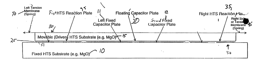
conventional prior art MEMS variable capacitors. Turning now to Figures 1 a
through 1 c,
a variable parallel split-plate capacitor tuned by a pair of magnetic
actuators with a
movable substrate 15 having a membrane-suspended vertical translational
geometry is
illustrated. The variable capacitor comprises a fixed substrate 10 suitable
for carrying an
HTS layer. Suitable materials for the fixed substrate 10 include MgO. On the
upper
surface of the fixed substrate 10, a first fixed capacitor plate 11 and a
second fixed
capacitor plate 12 are formed using thin-film HTS material. Such epitaxial
superconductive thin films are now routinely formed and commercially
available. See,
e.g., R. B. Hammond, et al., "Epitaxial TlzCa,BazCu208 Thin Films With Low 9.6
GHz
Surface Resistance at High Power and Above 77K", Appl. Phy. Lett., Vol. 57,
pp. 825-27,
1990. Adjacent to the fixed substrate 10 is a movable substrate 15 (drawn
transparent in
the plan view of Figure 1b) wherein the movable substrate 15 also comprises a
material
such as Mg0 suitable for deposition of an HTS layer. The variable capacitor
structure is
completed by the addition of a floating capacitor plate 20 on the lower
surface of the
floating plate 15 using thin-film HTS material. Floating plate 20 is spaced
apart and
CA 02401767 2002-08-29
WO 01/65629 PCT/USO1/05074
11
substantially parallel to the first and second fixed plates 11 and 12 and may
completely
cover the fixed plates 11 and 12 (thus forming a parallel split-plate
capacitor structure).
As a result, the HTS variable capacitor structure actually comprises two
variable
capacitors in series, which halves the capacitance per unit are over that of a
normal parallel
plate capacitor structure. The advantage is that no conductive contact to the
floating
capacitor plate 20 is required, a feature that greatly simplifies
(particularly for an HTS
implementation) the achievement of very low series resistance contact to the
capacitor,
thereby producing a higher Q. In such an embodiment, an input signal need be
coupled
only to the first and second fixed capacitor plates 11 and 12 through a pair
of signal leads
17 and 18.
A pair of magnetic actuators 30 varies the capacitance of the variable
capacitor by
increasing or decreasing a gap 25 between the floating capacitor plate 20 and
the first and
second fixed capacitor plates 11 and 12. The magnetic actuators 30 of the
present
invention utilize the property that a superconducting material cannot support
either an
electric or magnetic field within the bulk of the HTS material. If, for
example, an electric
field were impressed within a superconducting material, Ohm's law would demand
an
infinite current because the superconductor has no resistance. Conductors
subject to an
impressed magnetic field experience an induced electric field strength
proportional to the
rate of change of the magnetic field strength in the material, which generates
a transient
current in the material whose magnitude and duration depend on the
conductivity. In a
superconductive material, the do conductivity is infinite so that the duration
of this
transient current is infinite (" persistent" current). Because no magnetic
flux can penetrate
deeply into the superconductor, the persistent induced currents in the HTS
material will
flow in such a pattern as to ensure that this is the case. Thus,
superconducting materials
subject to an impressed field will generate "mirror" currents producing a
mirror field such
that the impressed field is opposed by the mirror field within the
superconductor material,
thereby avoiding the unnatural result of an infinite current. The magnetic
actuators 30
exploit this property by generating a magnetic flux which causes a magnetic
pressure to be
exerted on HTS reaction plates 35 on the lower surface of the movable
substrate 15. This
magnetic pressure or force may be opposed by a restoring spring force
generated by a first
and a second membrane 40 and 45 attached to either end of the movable
substrate 15 (the
weight of the movable substrate 15, assuming a vertical geometry, would also
provide a
restoring force) that would otherwise keep the gap 25 at a minimum value.
To generate the magnetic force, each magnetic actuator 30 has a magnetic
driver 50
comprising a continuous strip 51 of HTS material deposited on the upper
surface of the
fixed substrate 10. As illustrated in Figure 1b, the continuous strip 51 of
HTS material is
preferably arranged in a spiral drive coil. Note that as used herein, a
"continuous strip of
HTS material" will include within its scope a strip of HTS material that may
be
CA 02401767 2002-08-29
WO 01/65629 PCT/USO1/05074
12
interrupted by segments of non-HTS materials such as normal metals used in
overcrossings. In fact, the functionality of the invention would be the same
whether this
drive coil is a continuous superconductor, superconductor segments
interspersed with
normal metal segments (such as the overcrossing 54 from the center of the coil
to the
outside in Figure 1b), or entirely fabricated from normal metal. However, the
substantial
drive current power from a drive coil fabricated entirely from normal metal
could, in most
applications, cause a heat load sufficient to raise the device temperature and
cause the HTS
materials in the reaction plates and signal elements to be degraded, or to "go
normal"
entirely. This power dissipation problem is eliminated by having the drive
coils)
fabricated principally (or entirely) of HTS material.
An applied DC tuning current through the drive coil or continuous HTS strip 51
generates the repulsive magnetic force between the magnetic driver 50 and the
HTS
reaction plate 35. This repulsive magnetic force causes the gap 25 to increase
by an
amount determined by the applied tuning current, Id, the effective restoring
spring constant
produced by the first and second tension membranes 40 and 45, and the details
of the
magnetic field produced by the applied tuning current through the continuous
strip 51.
The details of the magnetic field will depend upon the arrangement of the
continuous strip
51. In a preferred embodiment, the strip 51 will be arranged into a planar
spiral drive coil
or other arrangements possessing a line of symmetry. As used herein, the
magnetic driver
50 is denoted a single pole driver, if on one side of the line of symmetry,
the current
through the sections of the strip 51 all flow in the same direction. In each
magnetic driver
50 of Figure 1b, the continuous strip 51 forms a single pole planar
rectangular "spiral"
coil using a single layer of HTS material. The rectangular spiral coil is
excited through
leads 52 and 53. Because the rectangular spiral coil is planar, the inner end
of the coil
must couple to lead 53 through an overcrossing (or possibly undercrossing) 54
formed in a
second conductor layer on the fixed substrate 10. As noted above, this second
conducting
layer from which the overcrossing 54 is fabricated can be of normal metal if
desired.
As illustrated in Figure 1 a, the continuous strip 51 is formed from a single
HTS
layer. The use of multiple (two or more) HTS layers in the magnetic driver 50
would
increase the force/cuirent sensitivity of the drivers if these benefits were
judged to offset
the added HTS technological complexity. It is to be noted that in the
embodiment
illustrated in Figures la and 1b, the reaction plates 35 may be solid plates
similar to the
plates used for the capacitor plates 11, 12, and 20. Such reaction plates will
only oppose
the magnetic flux created by the drive coils 50. Thus, the magnetic actuators
30 may be
denoted as "push" magnetic actuators. In other embodiments of the invention
discussed
herein, the solid reaction plates 35 are altered whereby magnetic flux trapped
in the
reaction plate allows either a repulsive force or an attractive force to be
created between
CA 02401767 2002-08-29
WO 01/65629 PCT/USO1/05074
13
the reaction plate and the drive coil - such embodiments of the magnetic
actuators may be
denoted "push-pull" actuators.
In the membrane-suspended geometry for the HTS tunable filter device
structures
of Figures la through lc having push-type magnetic actuators 30, any generated
magnetic
pressure is, in steady state, counterbalanced by the sum of the gravitational
force on the
movable substrate 15 (unless the plane of the movable substrate is exactly
vertical, in
which position this force is zero) plus the restoring spring force which is
provided by the
first and second tension membranes 40 and 45 extending from either end of the
movable
substrate 15 to posts 60 and 65 mounted on the fixed substrate (illustrated in
Figure 1 c).
To ensure that the tension membranes 40 and 45 return the movable substrate 15
to the
fixed substrate 10 in the absence of any tuning current in the magnetic driver
50, the posts
60 and 65 may be made slightly shorter than the thickness of the movable
substrate 15,
thereby achieving adequate response times, even in inverted operation such
that gravity
would tend to pull the movable substrate 1 S apart from the fixed substrate
10. Applying
current through the magnetic drivers (which would ordinarily be connected in
series as
illustrated in Figure 10b) creates a repulsive force which, if of adequate
magnitude, will
overcome the "spring" tension of the first and second tension membranes 40 and
45 and
the weight of the movable substrate 15, thereby increasing the gap 25 to a
given length z.
The striking differences between the forces produces by conventional
electrostatic
drivers for a MEMS capacitor versus those produced by the magnetic actuators
of the
present invention may be illustrated with reference to Figure 2. Figure 2
represents the
energy stored (per square centimeter of capacitor plate area) in both a
conventional
electrostatic MEMS driver and the magnetic actuator of the present invention
with respect
to the gap distance z defined between the capacitor plates. For an
electrostatic,driver
consisting of two parallel conductive plates separated by a gap, z, the stored
electric field
energy, Ee, (ignoring fringing) per unit area A between the plates having a
voltage
difference, V, will be given by
Ee /A = (E~/2) Ez z = (~~/2) (V/z)Z z = (E/2) VZ/z (Eq. 5)
where Eo = 8.854 x 10-'z Farad/meter (F/m) is the permittivity of a vacuum and
E = V/z is
the field strength. Note that the total electrostatic stored energy Ee falls
off as 1/z as the
gap size z is increased. The normal (z-direction) force per unit area, Fe /A,
between the
plates is just the derivative of Ee /A with respect to the gap z, or
Fe /A = d(Ee /A)/dz = -(E~/2)(V/z)Z (Eq. 6)
where the negative sign (from d(1/z)/dz = -1/z2) corresponds to an attractive
force between
the capacitor plates.
The extremely rapid fall off (as 1/z2) of electrostatic force vs. the gap
length z
contrasts dramatically with the force profile of the present invention.
Consider the
magnetic drivers 50 of Figure 1b each comprised of a continuous strip of HTS
material 51
CA 02401767 2002-08-29
WO 01/65629 PCT/USO1/05074
14
forming a closely spaced rectangular "spiral" coil. Within the coil, each
section of the
continuous strip 51 carries an identical current, Id, spaced by a gap z from
the HTS
reaction plates 35. The HTS continuous strip 51 is coiled according to a
pitch, P, which is
defined as the center-to-center distance between the sections of the coil. For
a gap z larger
than half of the conductor pitch P (i.e., for z >P/2), the magnetic field B in
the gap 25 will
be approximately parallel to the (planar) magnetic driver 50. Effectively,
with this
limitation on the pitch, the rectangular spiral coil within the magnetic
driver 50 acts as a
closed-loop uniform current sheet. When the lateral dimensions of the magnetic
driver 50
are much larger than the gap 25, the magnetic field strength, B, in the gap 25
is essentially
uniform and hence the (per unit volume) energy density (B~H/2) gives a per
unit area
magnetic energy density, En,/A, of
Em/A = (B~H /2) z = (1/2.0) BZ z (Eq. 7)
where ~o = 4n x 10-' H/m. Note that the total energy stored in the magnetic
field per unit
area E",/A increases in proportion to z as the gap size is increased. The
normal (z-
direction) force per unit area, Fm/A, between the planar coil in the magnetic
driver 50 and
the HTS reaction plate 35 is just the derivative of E",/A with respect to the
gap length z, or
F~,/A = d(Em/A)/dz = (1/2po) BZ (Eq. 8)
which means that the repulsive force is independent of the gap z (ignoring
fringing, which
will be true for gaps z substantially smaller than the lateral dimensions
(e.g., radius) of the
planar coil and HTS reaction plate 35). Thus, the magnetic driver of the
present invention
will provide a uniform force over a large range of gap displacements.
The energy approach just discussed gives a very good estimate for the magnetic
repulsive force for gap values greater than the pitch P, but substantially
smaller than the
overall lateral dimensions of the magnetic drivers and HTS reaction plates.
For a magnetic
driver having a single-layer planar coil, the wire pitch P (which is defined
as the center-to-
center distance between adjacent sections of the continuous strip of HTS
material) will be
the sum of the HTS section width, w, plus the spacing dimension, s, between
adjacent
sections. For example, P = 4.0 ~,m for w = 2.0 ~,m and s = 2.0 p.m. Since
typical
thickness values, tin, for commercially grown HTS layers are tn, =1.0 p.m, a
continuous
strip of HTS material with a w = 2.0 ~.m and an s =2.0 ~m represents a
lithographically
reasonable objective for fineline fabrication. These dimensions result in
conductor
sections having a cross-sectional area, A~, = 2 p,m x lam = 2 x 10-'2 m2 = 2 x
10~$ cm2. If
the maximum allowable current density, Jn,aX, in the HTS material is J",aX = 5
x106 a / cm2,
then the maximum conductor current would be (Id)maX 100 milliamperes (ma). If
a much
more conservative Jmax = 1.25 x10⁶ a / cm2 value were assumed, then the
maximum
conductor current would be assumed to be (I~maX 25 ma.
Application of a current Id to each conductor section in an array of N
parallel
conductors (with all currents in the same direction) having a conductor pitch
P and hence
CA 02401767 2002-08-29
WO 01/65629 PCT/USO1/05074
an array width W = NP, gives an effective current sheet of linear current
density, Id /W,
given by
Id /W = N Id /W = N Id /NP = Id /P [amperes per meter] (Eq. 9)
In turn, the transverse magnetic field, Hr, near an isolated array of
conductors or a current
5 sheet will have a magnitude (in amperes/meter or ampere-turns/meter) of
HT = (ampere turns [MMF])/(flux path length) = N I~ /2W = Id /(2P) (Eq. 10)
(since the shortest flux path length around a sheet of width W is 2W). The
notation H~ is
used for this transverse magnetic field, since is perpendicular to the axial
HZ field that is
usually of interest in coils (e.g., for calculating solenoid inductance,
etc.). In usual
10 practice, such a parallel array of conductors is bent around back on itself
in the plane of the
conductors to form a planar coil such as a planar spiral inductor when bent
into a circle. In
. this way the current from one turn is reused in the next, etc., so the
terminal current
required to produce N Id ampere turns of MMF is only Id amperes.
In the example of Figure la- lc, and the other embodiments illustrated herein,
this
15 "bending" is accomplished with four 90° corners to make a
rectangular or square planar
"spiral inductor", the behavior of which is very similar to that of a true
circular spiral of
the same area. The invention includes within its scope, however, any
configuration of the
continuous strip within the magnetic driver that produces a sufficient
magnetic force
between the driver and the reaction plate such that the movable substrate
moves with
respect to the fixed substrate. A magnetic driver having one planar coil
structure of this
spiral type (i.e., one in which all of the conductor sections on one side of a
plane of
symmetry through the coil carry current in the same direction) will be
referred to herein as
a single-pole driver. The planar coil of the magnetic driver is near the plane
of the HTS
reaction plate. The effect of the current flow (supercurrent) rejecting flux
penetration
through this HTS plane can be viewed as creating a mirrored image of the coil
on the other
side of the HTS plane. That is, if the planar coil is carrying current N Id
with the HTS
reaction plate a distance z from the coil, then the effect is the same as if
another coil
spaced a distance 2z from the coil were carrying a current -N Id. The magnetic
fields H
from these two coils add, making the magnetic field, Hr~ap, in the gap between
the coil and
the HTS reaction plate to be given by
Heap = H~ + H'T = N Id /W = Id /P (Eq. 11 )
where the " prime" on H'~ is to denote the magnetic field contribution from
the "mirrored"
coil on the other side of the HTS reaction plate (i.e., that due to the
supercurrent flowing in
the HTS reaction plate). The magnetic flux density, B=B~, generated in the gap
between
the planar coil and the HTS reaction plate will be given (for a relative
permeability of ~.~
=1)
Brgap = I~o H~ _ ~o Ia ~ (Eq. 12)
CA 02401767 2002-08-29
WO 01/65629 PCT/USO1/05074
16
which leads to, for gaps z greater than P/2, a repulsive force per unit area,
F",/A, between a
single pole coil and the HTS reaction plate of
Fm/A = (1/2.1,0) Brgap Z = (~..~.o /2) Id2/PZ (Eq. 13)
It is instructive to look at the magnitude of these magnetic flux densities
and forces in
practical cases of interest for HTS magnetic actuators. Table 1 illustrates
typical design
parameters under two sets of design rules; one "conservative," and the other
"more
aggressive" with respect to the coil current density JmaX, conductor section
spacing s, and
the thickness of the movable substrate, tms.
Table 1. Examples of HTS Driver Design Parameters
Current Density & Lithographic Design ConservativeMore
Rules:
Aggressive
Conductor Current Density, J~"~X (amps/cm2)1.25 x 106 5.0 x
106
Conductor Layer Thickness, tm (~.m) = 1.0 1.0
Conductor Width, w (gym) = 2.0 2.0
Conductor Spacing, s (p,m) = 2.0 1.0
Conductor Pitch, P (p,m) = 4.0 3.0
Maximum Conductor Current, ImaX(a) - Jt"aX 25 ma 100 ma
ws =
Flux Density in Gap at I = Imax, B~g (Gauss)78.5 Gauss 419 Gauss
=
Drive Force per Unit Area, Fn,/A (newtons/m2)24.54 N/m2 698 N/m2
=
Drive Force per Unit Area, F",/A (grams/cm2)0.25 g/cm2 7.12 g/cmz
=
Resulting Movable Substrate Kinetics:
Thickness of Movable Substrate, tms (p.m) 100 25
Mass per sq. cm (at Mg0 density of 3.5837g/cm')0.0358 g/cm28.96 mg/cmz
Max Acceleration of Movable Substrate, a 7.0 g's 795 g's
=
Minimum Time to Move ~z = 10 ~m (Rest 764 ~,s 71.6 ~,s
to Rest), ~t~ =
From Table 1, it may be observed that a (very) conservative Id = 25 ma drive
current with a P = 4pm conductor pitch gives a force, F",/A = 0.25g/cm2, for a
maximum
acceleration of a = 7.0 g's (68.45m/s2) of a tms = 4 mil (100~m) thick Mg0
substrate
(ignoring any membrane "spring" or gravitational forces). Using a more
aggressive Id =
100ma drive current with a P =3~.m conductor pitch gives a Fm/A = 7.12g/ cm2,
for a
maximum acceleration of a = 795 g's with a thinner, t"~ = 1 mil (25p,m) thick
Mg0
substrate.
The magnetic energy density approach to the calculation of the force
achievable
with an HTS magnetic driver used above has the simple elegance of energy
difference
calculations, along with their disadvantage of offering very little insight as
to just how the
force arises. Fortunately, it is not much more difficult to go back to
Ampere's law, which
CA 02401767 2002-08-29
WO 01/65629 PCT/USO1/05074
17
relates the (using bold face for the vector quantities) force F on a conductor
of length, l,
carrying a current of magnitude, I (in the direction of the length vector, 1),
in a magnetic
field B as
F = Il X B (Eq. 14)
Consider such a conductor running in the X-direction, spaced by a height, Z =
z
above a superconducting plane. The action of the superconductor in the Z = 0
plane will
be to support a current distribution such that no magnetic flux penetrates
this plane, which
is to say, BZ = 0 at Z = 0 (i.e., everywhere on the HTS plane). While the
supercurrent
distribution in the HTS plane to achieve this may be complicated, it is easy
to see that its
effect is exactly the same as if there were no HTS plane, but a conductor of
the same
length were placed an equal distance on the other side of the Z = 0 plane,
"mirroring" the
original conductor, but carrying current in the opposite direction (-I). (If
this is not
immediately obvious, draw a mental cross-section picture looking in the X-
direction,
showing identical conductor centers at Y = 0, Z= +/-z, with clockwise circular
field lines
around one and equal but counterclockwise field lines around the other
conductor. Where
these intersect on the Z = 0 plane, the transverse, By, field components add,
but the
vertical, BZ, components are equal but opposite, and hence cancel everywhere
on the Z = 0
plane.) This means that we can replace the HTS plane at Z = 0 with an
identical conductor,
carrying -I, at the mirror image position, Z = -z, and have the same effect on
forces, fields,
inductances, etc. as the HTS plane has. This applies, by extension, to any
number of
conductors in any orientation, such as loops, coils, etc.
Consider the case of a planar array of conductors of length, 1 =lX, carrying
identical
currents, I, having a pitch P at a height Z = z above the HTS plane (Z =0).
While there is a
Y-component of force causing the conductors to attract one another (we assume
they are
firmly mounted to the fixed substrate so no motion results from Fy), absent
the nearby
HTS plane, there would be no transverse component of magnetic field in the
plane of the
conductors (i.e., Hr = HX = HY = 0 at Z = z without the HTS plane), which
would mean (due
to the cross-product in Eq. 14) that there could be no Z-component of force on
the
conductors. The Hy transverse field component from all of these conductor
currents does
exist above and below the Z = z plane of the conductors, and in fact is just
that given
earlier in the equation for Hr. While the HY (or Hr for radial) component in
the Z = z plane
containing the conductor array is zero because of symmetry (HY is changing
sign from
+I/(2P) to -I/(2p) right at Z = z), this is not the case when the symmetry is
broken by the
addition of the HTS plane at Z = 0. The magnetic field from the conductor
array mirrored
at Z = -z indeed has a strong transverse, Hy, component, as described above.
As a result,
with the HTS plane present, there is a transverse, BY, flux density at the Z =
+z plane of
conductors, given by
BY = ELo Hy = p.o NI/(2W)= (11o /2)~' (Eq. 15)
CA 02401767 2002-08-29
WO 01/65629 PCT/USO1/05074
18
From Eq. 14, the result of the B = By magnetic flux density acting on a X-
oriented wire of
length 1= 1X carrying a current I will be a z-direction force, FZ, (per wire)
given by
FZ (per wire) _ (I 1X) BY = (I 1X) (~.o /2) I/P = (~.o /2) lx IZ/p (Eq. 16)
The total repulsive force between the N conductor array (whose width in the Y-
direction is
S Wy= NP) and the HTS plane will be N times this, or
F = FZ = N (!-to /2) 1X IZ/P = (W~/P) (I-Lo /2) 1X Iz/P = (N-o /2) (WY 1X)
IZn'2 (Eq. 17)
The quantity Wy 1X is, of course, just the area A of the driver array, so the
force per unit
area, F~/A, on the "coil" is given by
F~/A = (~,o /2) Iz/Pz (For z>P/2 and D»z) (Eq. 18)
where D is the lateral dimension of the array. This is the same expression for
force per
unit area as derived using the field energy approach in Eq. 13.
More detailed analyses of the z-dependence of the single-pole force, as well
as
Fm(z) for multi-pole driver "coils" (such as meander lines) in which not all
of the
conductor currents flow in the same direction can be based on the detailed
conductor-to-
conductor force relationship, and then summing these over all the conductors
in the array.
From Eq. 14, it can be shown that if two circular cross-section parallel wires
of length 1
separated by a distance r carry currents I, and Iz then the force per unit
length, F,2, between
them (using "-" sign for attractive force) is given by
F,2/1= -(p.o /27L) (I, IZ)/r = -2x 10-' (I, IZ)/r (Eq. 19)
As noted previously, in a single-pole planar driver coil in a magnetic driver
of the type
illustrated in Figure 1b, the currents in adjacent turns are equal and in the
same direction,
resulting in substantial attractive forces between the turns. But these
attractive forces are
only in the plane of the coil (transverse, or "radial" direction of a spiral),
not in the vertical,
Z-direction. On the other hand, the currents in the conductors "mirrored" at Z
= -z on the
opposite side of the HTS plane are in the opposite direction, IZ = - I" so the
force will be
repulsive, and, since the "mirrored" coil and the drive coil are not in the
same plane, there
will be a Z-component of this F,Z /1 force. For a planar array of conductors
in the coil
carrying identical currents I at a pitch P, the Z-component of force on a
conductor, i, is
obtained from Eq. 18 by summing all of the contributions from each of the
array
conductors, j', "mirrored" in the HTS plane. For example, the force
contribution to
conductor i from its own image at Z =-z (or r = 2z away from the conductor)
will be purely
vertical, repulsive, and given by
FZ;;JI = (~o /2~) Iz/ (2z) = 2 x 10-' Iz/ (2z) (Eq. 20)
The total Z-component of force on conductor i is obtained by summing the
vertical
components of force due to all of the mirrored conductors j' (including
itself; the simple
j'=i' case given in Eq. 20). This summed total force on conductor i is given
by
Fz;/1= ~Iz (N.o 12nx2z~l ~2z~ +~~j'-i~P~ Eq. 21
J,
CA 02401767 2002-08-29
WO 01/65629 PCT/USO1/05074
19
All of the terms of this sum over j' are positive (repulsive force) if all of
the currents in the
conductor array are in the same direction (single pole magnetic driver). This
type of sum
calculation is easily carned out in a spreadsheet calculation (Microsoft Excel
was used for
most of the results shown here). Figure 3 shows the force (per meter of wire
length) on the
center wire (the center section of the continuous strip of HTS material
forming the planar
spiral coil) in a field of 201 wires, all carrying unit current (I = 1.0
ampere) in the same
direction, versus the height, z, of this planar "coil" above the HTS plane,
for various values
of the wire pitch, P. This force is essentially constant for z>P/2, and in
this "flat" region is
inversely proportional to P with magnitude as given by Eq. 16 (with I=1 ampere
and lx =1
meter).
For a multi-pole driver in which the current directions are reversed
periodically,
Eq. 21 is used, but it is necessary to keep track of the alternating signs of
the terms in the
sum. Turning now to Figure 4, a pair of mufti-pole magnetic drivers 70 is
illustrated.
With the exception of the configuration of the continuous strip 51 within the
magnetic
driver 70, the embodiment illustrated in Figure 4 is identical to that
illustrated in Figure
lb. As used herein, if the continuous strip of a magnetic driver is arranged
in a
configuration having a line of symmetry and the current through parallel
sections of the
continuous strip on the same side of the line of symmetry travel in different
directions, the
magnetic driver is denoted a "mufti-pole" driver. In the extreme mufti-pole
case of a
meander line mufti-pole magnetic driver, such as illustrated in Figure 4,
adjacent sections
of the continuous strip of HTS material carry current traveling in opposite
directions,
which means that the j' = i term (Eq. 20) and all of the other terms for which
(j'-i) is even
are positive, but all of the terms in Eq. 21 for which (j'-i) is odd are
negative. Figure 5
shows a force vs. z plot similar to that of the single-pole case of Figure 3,
except that the
currents are reversed in groups of wires in a mufti-pole pattern. In all cases
in Figure 5, a
basic wire pitch of P=2.0 ~m is assumed, so that if all the currents were in
the same
direction, the FZ(z) force would be the same as the top curve in Figure 3,
flattening off at a
(per wire) value of 0.314 newtons/meter/amperez. The various curves in Figure
5
correspond to different magnetic pole dimensions , Pm, where Pm is the
distance across the
parallel conductors in the array before the current reverses sign. For
example, in the
simplest case of a meander line, as seen in Figure 4, the current reverses
every conductor,
so for the P = 2.O~m wire pitch case illustrated, the magnetic pole pitch of a
meander line
is Pm = 2.O~.m. Correspondingly, the Pm =6p,m curve in Figure 5 is for a
repeating pattern
of three wires with +I followed by three wires with -I, etc., on to 1 S wires
with +I and 15
wires with -I for the Pm = 30~m curve. Of note is the fact that, other than
for the Pm _
2.Op.m case, all of the curves fall to about the same (per wire) force value
(FZ 0.0175
newtons/meter/ampere2 ) at a "coil" height, z, above the HTS plane equal to
half the
magnetic pole dimensions Pn, (i.e., at z= Pm /2).
CA 02401767 2002-08-29
WO 01/65629 PCT/USO1/05074
The rapid FZ(z) fall-off of repulsive force with height, which is controllable
by
selecting the magnetic pole size Pm could prove of substantial value in some
driver
applications, such as open-loop operation over a carefully controlled height
range. (As
used herein, open-loop operation refers to the use of a variable tuning
current, Id, through
5 the planar driver coil to produce the desired gap, z, without the use of a
height sensor
element on the movable substrate to control z by means of a feedback control
system.) For
many applications, however, principal interest would be in achieving the
greatest force
over a large z motion range, for which simple single-pole drivers (spiral
inductor-type
coils) coils excel. For the remaining tunable filter element examples
discussed below,
10 single-pole magnetic drivers will be illustrated, but that is not to imply
that the use of
mufti-pole driver configurations might not be more suitable in some
applications.
It is important to point out one artifact in the FZ(z) curves in Figures 3 and
5. The
very rapid, 1/z, rise in FZ(z) for z<0.5 ~,m is an artifact of the assumption
of infinitesimal,
or very small circular cross-section to the conductor wires in the planar
coil. In this
15 assumption, the magnetic field strength, Be(r), at radius r from the center
of an isolated
conductor carrying a current I is given by
Be(r) _ ~o I/(2~r) (for r > conductor radius) (Eq. 22)
For an HTS magnetic driver, at very small gaps z, each conductor becomes very
close to
its own mirror image r = 2z away, and hence sees a very large magnetic field
By = Be(2z)
20 from Eq. 22, leading to the 1/2z singularity of force, FZ;;./I, in Eq. 19
as z approaches zero.
In practice, the sections of the continuous HTS strip forming the planar coil
in the
magnetic driver may be lithographically patterned from deposited planar
conductor layers,
and hence tend to be of rectangular cross section, typically (as shown in
Table 1) with a
width w substantially greater than the thickness tm. For an isolated
rectangular conductor
carrying a current I, the average magnetic field strength around the periphery
of the
conductor will be
BAvg ~ ~o I/(2w+2t",) (near surface of rectangular conductor) Eq. 23
While at large distances, r » w, from the center of the rectangular conductor,
Eq. 22 will
approximate the field, for small gaps z, the field strength, and hence the
repulsive force,
does not increase as 1/(2z) as in Eqs. 22 and 20, but rather saturates toward
a constant
value.
The previous examples and performance analyses of all-HTS magnetic actuators
for the implementation of variable reactive elements for tunable filters and
other
applications were based on the magnetic repulsion between a planar driver coil
and a
superconducting plate. However, it would be possible to implement such
configurations
using normal metal conductors, as long as ac drive currents, Ia, were used of
a sufficiently
high frequency that the skin depth in the reaction plate is substantially less
than its
thickness. If, however, a configuration using normal metal conductors was
implemented
CA 02401767 2002-08-29
WO 01/65629 PCT/USO1/05074
21
using the "more aggressive" actuator design rules column from Table 1 with t",
= 2.Op.m
thick copper at a room temperature resistivity of 1.70 p.S2-cm, the power
dissipation in the
coil, at I = 100ma would exceed 14 watts per square millimeter (actually well
above this
due to increased ac skin-effect conductor losses). The ac eddy current losses
in the
reaction plate would be only slightly less than this, and there is virtually
no thermal
conduction path away from the movable substrate to get rid of this heat. The
previous
examples and performance analysis of all-HTS magnetic actuators for the
implementation
of variable reactive elements for tunable filters and other applications were
based on the
magnetic repulsion between a planar driver coil and a superconducting plate.
However, it
would be possible to implement such configurations using normal metal
conductors, as
long as ac drive currents, Id, were used of a sufficiently high frequency that
the skin depth
in the reaction plate is substantially less than its thickness. If, however, a
configuration
using normal metal conductors was implemented using the "more aggressive"
actuator
design rules column from Table 1 with tm = 2.Op,m thick copper at a room
temperature
1 S resistivity of 1.70 p.S2-cm, the power dissipation in the coil, at I =
100ma would exceed 14
watts per square millimeter (actually well above this due to increased ac skin-
effect
conductor losses). The ac eddy current losses in the reaction plate would be
only slightly
less than this, and there is virtually no thermal conduction path away from
the movable
substrate to get rid of this heat. Hence, the use of normal metal conductors
for the drive
coils and reaction plates, while theoretically possible for a repulsive
driver, is thermally
impractical.
A desirable characteristic for actuators would be a push-pull actuator
technology.
In a push-pull driver application, very little mechanical "spring" restoring
force would be
required, and it would be possible to pass substantial levels of drive current
Id only when
the position of the movable substrate is to be changed. (With minimal spring
restoring
force, closed-loop feedback stabilization of the position z of the movable
substrate would
be utilized. In such a configuration, higher levels of drive current would be
dictated by the
feedback control system only when substantial errors between the actual sensed
position
and the desired position of the movable substrate were sensed.) This approach
would offer
very low power dissipation in the control electronics (the power dissipation
in the HTS
drive coils and reaction plates being extremely small anyway), and potentially
substantially less noise or fluctuations in movable substrate position, z, due
to noise in the
current drive electronics (fluctuations in z could translate into phase noise
on signals). As
will be discussed herein, it is possible to implement the effect of a push-
pull driver
mechanically, by means, for example, of locating drive coils on opposite sides
of the HTS
reaction plate on the movable substrate. Another embodiment of the invention
utilizes a
rotational approach, preferably implemented with a torsion suspension fiber or
band
suspending the movable substrate above the fixed substrate in a "teeter-
totter" type of
CA 02401767 2002-08-29
WO 01/65629 PCT/USO1/05074
22
geometry, with a repulsion "push" driver under each end of the movable
substrate on
opposite sides of the suspension band. This type of "push-push" configuration
may
emulate the effect of a true repulsive-attractive "push-pull" driver, but
requires additional
mechanical and fabricational complexity.
Because of the unique characteristic of superconductors to sustain a
supercurrent
after the source that excited the supercurrent is removed, it is possible to
reconfigure the
reaction plate to enable a true "push-pull" repulsive-attractive HTS driver to
be realized. If
a superconducting loop contains an initial amount of magnetic flux, ~P, such
as flux
present in the loop when it entered the superconducting state, the action of
the
superconductor will be to maintain the amount of enclosed flux constant at ~P
thereafter.
A "push-pull" HTS driver approach utilizing this characteristic of
superconductors
to achieve a true repulsive-attractive magnetic force driver is illustrated in
Figure 6.
Illustrated at the top of Figure 6 is a "push" (repulsive) magnetic driver 50
with its solid
HTS reaction plate 35. Since it starts, presumably, with no trapped flux, ~p =
0, the
application of a given level of current, Id, to the magnetic driver 50 in
close proximity, Z =
z, to the solid HTS reaction plate 35 generates an equivalent opposite
("mirror")
supercurrent, Im - Id in the HTS plane (wherein Im is defined as the
equivalent current in
the "mirror image" coil at Z = -z that produces the magnetic flux densities
and FZ(z) forces
previously discussed). To implement a "push-pull" driver, the present
invention requires
a reaction plate that is not only capable of supporting the Im - Id "mirror"
currents, but is
also capable of supporting stored flux levels, gyp, as well. Shown at the
bottom of Figure 6
is an example of an HTS reaction plate 75 capable of doing this. This HTS
reaction plate
75 is comprised of a series of concentric HTS loops 80 that generally match
the patterm
(i.e., general shape, not necessarily detailed pitch, etc.) of the loops in
the matching drive
coil. Because the conductor pattern in the HTS reaction plate 75 follows the
direction of
the sections of the HTS continuous strip 51 in the magnetic driver 50, it
should efficiently
support the Im - Id "mirror" current when a current, Ia, is passed through the
magnetic
driver 50. In addition, because the reaction plate is comprised of a plurality
of concentric
HTS loops 80 , each one of which is capable of storing magnetic flux, gyp, the
reaction
plate 75 should be capable of storing flux as desired for the " push-pull"
driver.
Just as the easiest way to understand the behavior of the repulsive "push"
magnetic
driver is to replace the HTS reaction plate by the "mirror" coil at Z = -z
from the planar
coil in the magnetic driver at Z = +z, the "mirror" coil behavior is the
easiest way to look
at this "push-pull" driver. The key difference in the "'push-pull" case is
that the "mirror"
current, Im is not simply the opposite of the drive coil current, Im = -Id, as
it is in the "push",
solid HTS reaction plate, case. Rather, in the presence of stored flux in the
reaction plate,
the "mirror" current Im will be given by
Im = Ip - Ia (with stored flux in HTS plate) (Eq. 24)
CA 02401767 2002-08-29
WO 01/65629 PCT/USO1/05074
23
What Eq. 24 indicates is that in the absence of any driver current, Id, there
is still an
equivalent current, Im = Ip in the "mirror" coil at -z. This quantity, Ip, is,
of course, the
effective value of the supercurrent required to maintain the magnetic flux
trapped in the
HTS reaction plate constant at its ~p initial value. It is useful to refer to
Ip as "poled
S current" in the HTS reaction plate, and the process of storing the magnetic
flux, ~P, in the
plate as "poling", in analogy to the poling process of applying a strong
electric
field/temperature to a ferroelectric material to make it piezoelectric (as
opposed to just
electrostrictive). The poling process is used in a ferroelectric to break down
the electric
field directional symmetry. When the positive and negative electric field
directions are
indistinguishable, the elongation can only vary as the square of the electric
field,
analogous to the IZ behavior of force for the "push" magnetic driver (e.g.,
Eq. 18). By
creating a preferred direction of electric field, so that positive and
negative field directions
are discernable, the ferroelectric material may become piezoelectric; that is,
it may have a
first-order (linear) term in its elongation vs. voltage curve. The magnetic
"poling" process
has the same effect in this "push-pull" driver configuration. With no trapped
flux in the
reaction plate, there is no difference between +Ia and -Id drive currents, and
hence the FZ(z)
force must vary as Id2 (or higher even power terms). With the reaction plate
"poled", the
polarity of IP establishes a difference between +Id and -Id drive current
directions, and
hence the FZ(z) force can have linear (FZ(z) ~ I~ or higher odd-order terms
(in addition to
even-order terms). This can be most easily seen by writing the proportionality
between the
force, F, the drive coil current, Id, and the "mirror" coil current, Im, and
then substituting in
Im = Ip - Id (Eq. 24) as
FZ = k Id Im = k Id (IP - Id) (with poled current, IP) Eq. 25
Turning now to Figures 7a and 7b, a comparison of the generated magnetic force
for a given current through the magnetic driver for both push and push-pull
magnetic
actuators can be made. The FZ(I~ curve for Ip = 0 in Figure 7a shows the usual
"push",
pure-repulsive FZ proportional to Id2 force relationship (parabola centered at
Id = 0). When
the HTS reaction plate is "poled" with an equivalent "mirror" current, Ip, as
in Figure 7b,
the parabola is shifted to Ia = IP /2, with zero force points, FZ = 0, at both
Id = 0 and Id = Ip,
with attractive force between these points, 0 < Id < Ip, and repulsive force
outside of this
region.
Repulsive force Id operation range: Id < 0
Attractive force drive current range: 0 < Id < Ip
Repulsive force "overdrive" Id range: Id > IP
Normal "Push-Pull" Operation Range - IP < Id < IP /2 Eq. 26
There is indeed a first-order dependence of FZ (I~ near Id = 0 with
substantial levels of
attractive force available. In addition to achieving "push-pull" driver
operation, "poling"
the HTS reaction plate can substantially increase the driver current
sensitivity. For
CA 02401767 2002-08-29
WO 01/65629 PCT/USO1/05074
24
example, in the illustration of Figure 7b, in the IP = 0 driver curve, a
driver current in either
direction of 1 division gives a repulsive force of 0.25 divisions, whereas in
the Ip = +3
divisions curve, a driver current of Id = -1 division gives a repulsive force
of 1 division,
while an Id = +1 division driver current gives an attractive force of 0.5
divisions. The more
heavily the HTS reaction plate is poled (i.e., the greater the magnitude of
Ip, the greater the
current sensitivity, (FZ /Id), and the greater the magnitude of attractive
force which can be
realized in the "push-pull" driver.
Of great practical interest is the issue of how best to accomplish the
magnetic
"poling" of the patterned HTS reaction plates in an array of tunable elements
using these
push-pull drivers. One method of poling the HTS reaction plate, would be to
apply a drive
coil current, Id = Ip while the HTS reaction plate is cooling down through its
critical
temperature (with the coil and plate in close proximity, of course). Applying
a high level
of drive current requires, of course, that the HTS drive coil be well below
its critical
superconducting temperature. On the other hand, at the start of the poling
process, the HTS
reaction plate must be above its critical temperature, T~. This could, in
principal be
achieved by using, for example, TBCCO ("Thallium"), with T~ = 92° K,
for the coils, and
"YBCO" with a T° about 10° K lower for the reaction plates.
However, it is preferable that
the coil temperature be as low as practical during the poling process to make
the poled
current, Ip, as high as possible. Also, it would be much more convenient to
use the same
HTS material for the entire device structure.
In an embodiment of the invention using the same HTS material in the magnetic
driver and the reaction plate, it would be necessary to have a transient
temperature
difference between the HTS reaction plates and the HTS magnetic drivers during
this
poling process. Because the HTS planar coils of the magnetic drivers are on
the fixed
substrates which should have a good thermal path to the cryo-cooler head,
while the HTS
reaction plates (being on the movable substrate) have a relatively poor
thermal path
(relatively high thermal resistance) down to the fixed substrate, the present
invention may
exploit these thermal path differences. An extremely simple, exploitation of
this would be
to carry out the poling during the initial cooldown process; due to the better
thermal path
to the fixed substrate, the drive coils should become superconducting well
before the HTS
reaction plates on the movable substrates do. A more practical, but still very
simple,
approach would be to enclose a filament heater in a vacuum enclosure above the
HTS
substrate (with the movable substrate side facing the heater). After the both
substrates are
cooled down fully, the poling process would be initiated by briefly flooding
the movable
substrate with radiant energy from the heater. Because of the large thermal
mass and high
thermal conductivity path of the fixed substrate, the temperature rise in the
HTS driver
coils would be negligible. On the other hand, because of the low thermal mass
and high
thermal resistance of the movable substrates, they would quickly rise in
temperature to
CA 02401767 2002-08-29
WO 01/65629 PCT/USO1/05074
above the T~ of the HTS material, at which point the heater would be turned
off. The
poling of all of the "push-pull" driver reaction plates would be accomplished
by applying
the desired poling current, Ip, (usually using the largest coil current
practicable) during the
period when the movable substrates are cooling back down from their T> T~
transient
5 temperature to their original T« T~ temperature. An alternative to this
"general radiant
flood" approach for simultaneously poling all of the drivers on the substrate
(and
temporarily disabling the rf functionality of all of the tunable devices on
the substrate)
would be to selectively apply transient radiant heating pulses to individual
devices from
one or more directed source(s), such as lasers or light-emitting diodes. An
additional
10 thermal poling approach, which could be applied selectively, would be to
apply current
through a resistive element (heater) on each individual movable substrate.
This could in
fact be quite simple to implement. For example, a number of the mechanical
designs of
interest feature a rotational geometry, which would typically use a torsional
suspension. If
a thin carbon fiber, fine metallic wire, or metallized polymer membrane were
used to
15 implement this suspension, then simply passing a suitable level of current
through this
suspension wire could be used to heat the movable substrates above T~. This
same
approach could be used with the vertical translational geometry illustrated in
Figure 1 a by
metallizing all or part of the suspension membrane.
In these transient temperature approaches to the magnetic poling of the HTS
20 reaction plates, the time required for the poling operation will be
determined by the
transient cooldown time of the movable substrates in the environment where the
fixed
substrate and rest of the enclosure is fully cooled. Because of the small
thermal mass of
the thin movable substrates, this time should not be too long, but the poor
thermal
conduction path from the movable substrates to the fixed substrate and the
reduced
25 effectiveness of radiant heat transfer at cryogenic temperatures will make
this cooldown
longer in some cases. This would particularly be true if it proved necessary
to re-pole the
HTS reaction plates fairly frequently, as might be the case if the storage of
very high flux
levels were attempted.
In some applications where the time required to re-tune the HTS tunable filter
elements is critical, achieving the maximum possible force levels out of the
HTS drivers
would be sought. In such cases, it would be desirable, for purposes of
achieving
maximum current sensitivity, (F~/Id), and magnitude of attractive force, that
the poling
current, IP, or flux, ~P, level be as high as possible. At high flux levels in
HTS materials it
is possible for flux to slowly escape from superconducting loops ("flux
creep"), which
could necessitate re-poling the HTS reaction plates at some interval to
maintain the value
of Ip at the desired level. While the somewhat limited levels of poled
current, Ip, which it
would be safe and practical to induce in the HTS reaction plates by passing a
current, Id =
Ip through the drive coils during the poling operation may not be sufficient
to make flux
CA 02401767 2002-08-29
WO 01/65629 PCT/USO1/05074
26
leakage a significant problem, it would be preferable to be able to achieve
much higher Ip
levels, and in that case fairly frequent "recharging" (re-poling) of the
reaction plates might
be needed.
A potential method for achieving very high flux levels in the HTS reaction
plates
for "push-pull" drivers, as well as the capability for very rapid re-poling,
would be the
application of a high-intensity pulsed magnetic field to the entire HTS
structure. If a more
or less uniform external magnetic field, H~" is applied to the entire array of
tunable HTS
devices at a peak transient magnetic field intensity well above the critical
field, H~, of the
HTS superconductor material, then in effect the HTS loops in the "push-pull"
HTS
reaction plates will be momentarily be driven normal, with high levels of flux
driven into
the loops, even though they remain at a temperature well below T~. As the
transient
external pulsed field dies out, however, the flux levels within the loops will
very rapidly
die out to a level sustainable given the H~ of the HTS material. The stored
flux, ~P, or
equivalent poling current, Ip, levels achievable using pulsed external field
poling should be
considerably greater than achievable by thermal transient poling through the
drive coils. It
should be noted that the use of a large external magnetic field, H~, » H~,
oriented in the
axial (Z) direction would not necessarily end up with the same distribution of
currents
among the concentric loops in the HTS reaction plates as poling through the
drive coils
does. The empirical definition of the equivalent "mirror" poling current, IP,
in this case
would be by reference to the "push-pull" force expression, Eq. 24, in which
FZ(I~ is
parabolic, with the attractive force region bounded by zero force points at Id
= 0 and Id = Ip.
It is notable that the purpose of the "poling" process in the "push-pull"
driver is to
turn the HTS reaction plate into a type of permanent magnet. In an alternate
embodiment
of the invention, the HTS reaction plate may incorporate a permanent magnet
material
instead of captured circulating supercurrent. While this embodiment of the
invention
avoids the need for poling the HTS reaction plate, it introduces the
complication of
bringing a mixture of different technologies into play. In addition to the HTS
materials
technology, an efficient cryogenic temperature ferromagnetic material
fabricationally
compatible with the HTS material would be required. Another difficulty is that
the
magnetic poling pattern required for best performance with such a
ferromagnetic reaction
plate is rather complicated. To match the rectangular spiral planar coil
configuration of
Figure 6, four wedge-shaped permanent magnet segments poled parallel to the
surface and
radially toward the center of the planar coil would be optimal.
The absolute force relationships for the all-HTS "push-pull" driver can be
obtained
by extension from the earlier pure-repulsive ("push") driver analysis. Note
that with no
current poled into the HTS reaction plate, the "push-pull" case of Eq. 25
reduces to the
same FZ = -k Id2 relationship determined previously (e.g., Eqs. 13 and 18) for
the "push"
only drivers. Since the force constant, k, must be independent of Ip,
comparing Eq. 25
CA 02401767 2002-08-29
WO 01/65629 PCT/USO1/05074
27
with IP = 0, [FZ = -k Idz], to Eqs. 13 or 18, [FZ = A(~,o /2) Id2 !P2] gives k
= - A(~o /2) / Pz for
the constant (where the "-" sign is from our convention of a repulsive force
being taken as
positive). This gives for the "push-pull" driver force
FZ /A = [-(po /2) PZ] Id (Id - Ip) (For z >P/2 and D»z) Eq. 27
Regardless of whether the magnetic actuator of the present invention is of the
"push" or "push-pull" type, a mechanical means may be used to restore the
movable
substrate into position with respect to the fixed substrate after an
adjustment by the
magnetic actuator. As discussed with respect to the vertical translational
configuration of
Figures 1 a and 1 c, a restoring force may be provided by a first and a second
membrane 40
and 45 attached to either end of the movable substrate 15. The mechanical
aspects of this
design are further illustrated in Figure 8 wherein the heights of the two
membrane support
posts 60 and 65 are equal to the thickness of the movable substrate 15 (i.e.,
zo~.se, - 0 where
zorrset denotes the rest gap length between the fixed and movable substrates
when no tuning
current flows through the magnetic actuators (FZ = 0)). Should the post
heights, tpos" be
greater than the thickness of the movable substrate, tmsub~ then the rest
position of the
substrate with no magnetic driver force, FZ, applied (ignoring the
gravitational force on the
moving substrate) will be at a gap
z = zo~.se~ = tpos~ - tmsub (rest position for FZ = 0 for zo,.fse, >_ 0) Eq.
28
In embodiments of the invention in which the posts are shorter than the
movable substrate,
zo~.se~ is negative and the actual rest position will be at z = 0 due to
contact between the
movable substrate and the fixed substrate, but as long as FZ is such that z >
0, the "spring"
force expressions are all valid for negative values of zo~.se,. (In fact, if
pure repulsive
drivers were used, particularly with feedback positional control, then
negative zo,~Se~ values
would typically be utilized to insure the availability of adequate restoring
force at small
values of z to allow for fast response.) The principal "spring" restoring
force in this
embodiment comes from the initial tension, Tn" in the membrane (where Tm is
the force
per unit width in the direction between the movable substrate and posts in
units of newtons
per meter). For a width, Wm, of the membrane, the tensile force in the
membrane support,
FS, will be given by
FS = Wm Tm (newtons) Eq. 29
At a substrate position (gap), z, the angle, ~, of the membrane support will
be given from z
and the length of the membrane between post and movable substrate, 15, by
~ = ArcTan [(z - zo~.se~/ 15] (membrane angle) Eq. 30
This places a downward force on the movable substrate, FS Sin(), that opposes
the upward
(repulsive) force from the magnetic driver, FZ. The balance condition between
these two
forces will be
FZ = FS Sin() = FS Sin {[ArcTan [(z - zo,~se~/ 1s)]} ~ FS [(z - zo~.se~/ 15]
Eq. 31
CA 02401767 2002-08-29
WO 01/65629 PCT/USO1/05074
28
The latter approximation is valid for small angles, ~, where Sin() = Tan() _
~, in which
range the membrane tension, Tm, and force, FS, are virtually independent of z.
The steady-
state movable substrate deflection, z - zo~.se" achievable with a drive force,
FZ, will be given
by
(z - zo~.se~- (1s/ FS) FZ (steady-state deflection) Eq. 32
The open-loop dynamics of this type of translational movable substrate depend
on
the type of magnetic driver used. If a mufti-pole driver of the type shown in
Figures 4 and
5, which itself has a steep FZ (z) curve, the effective spring constant for
oscillation will be
dominated, at least for strong drive currents, Id, by the FZ (z) of the
driver. For single-pole
magnetic drivers, however, the FZ (z) curves, as illustrated in Figure 3, tend
to be quite flat
(FZ = independent of z) over most of the range of interest. In that case, the
effective spring
constant, Kz, operating on half of the mass of the moving substrate, Mms /2,
(half, because
of the choice in Figure 8 and Eqs. 28 to 30 to treat the driver and suspension
forces on one
side [e.g., left side driver and membrane forces] only) will be given by
ICz = dF/dz = FS / is (for compliant driver FZ (z)) Eq. 33
The open-loop mechanical oscillation frequency, Fos~, for the M",s /2 mass
with this support
spring constant, KZ, will be given by
Fos~ _ (1/2~) Sqrt[Kz /( Mn,s /2)] _ (1/2~) Sqrt(2 FS / is Mms) Eq. 34
The quantity FS / is is a design parameter of the support membrane set
principally, from Eq.
31, by the desired maximum deflection range, OzmaX and maximum available
driver force,
(FZ)maX bY FS / is = ((FZ)max / ~Zmax ~ so that Eq. 34 may also be written as
Fos~ _ (1/2~) Sqrt [2 (FZ)max /(~ZmaxMms)] Eq. 35
Using the (FZ)maX values from Table 1, and assuming a Ozmax =10~m deflection
range is
desired gives, for the "conservative" design rules an open-loop mechanical
resonant
frequency of Fos~ = 416 Hz, while for the "more aggressive" design rules, a
higher, Fos~ _
4.44 kHz, resonant frequency would be realized.
It is possible to operate a device of this membrane suspended vertical
translational
geometry with "push" magnetic drivers in an open-loop mode, in which the
tuning is
selected by simply forcing a given drive current, Id, through the drive coils,
generating a
magnetic drive force, FI"Z(Id,z), and waiting for the motion of the movable
substrate to
bring the sum of the gravitational and spring restoring forces into balance
with Fm(Id,z).
Unfortunately, the settling time after Id tuning changes in such open-loop
operation can be
quite substantial, particularly if the mechanical Q of the translational
oscillation of the
movable substrate is high (which is equivalent to saying its mechanical
damping factor is
low). To achieve a final tuning precision corresponding to a small fraction of
the tuning
change, the settling time required is much greater than the product of the
mechanical Q
times the period of mechanical oscillation (or Tsett,~~g » Qm/Fos~). Open-loop
operation is
also very susceptible to tuning frequency shifts induced by changes in
gravitational
CA 02401767 2002-08-29
WO 01/65629 PCT/USO1/05074
29
orientation or external acceleration (vibration or "microphonic") effects.
Hence, open-
loop tuning would not be optimal for applications in which very rapid tuning,
and freedom
from detuning in the presence of gravitational or other acceleration changes
is desirable
during operation. In closed-loop operation, with high loop gain, it is
possible to approach
pure acceleration-limited positional transition times, T, (rest-to-rest) as
given for equal
maximum +z and -z accelerations, aZ+ = aZ_ = aZ for a displacement distance,
0z, as
T = Sqrt (4 ~z / aZ) (acceleration limited) Eq. 36
Table 1 includes typical values for T for the driver embodiments discussed
therein. Note
that with a "push-pull" driver, the mechanical design strategies for best
performance in
feedback operation is to use the most compliant practical suspension (lowest
value of FS /
1s), which will give a very low natural frequency, Fo~~, but also the lowest
level of "wasted"
forces driving the suspension "spring". The closed-loop operating frequencies
will be far
beyond Fo~~, dictated principally by the acceleration-limited time, T. In the
case of a pure-
repulsive driver, the -z force must be provided by the suspension. If equal
positive and
negative accelerations were to be achieved, half of the maximum repulsive
driver force
would be used to offset the suspension spring force, so the available
acceleration in Eq. 35
would be reduced by a factor of two. Again, however, it is desirable to have
maximum
spring compliance (for minimum change in this spring force over the travel
range), so that
typically a negative value of zo~.se~ would be used for this type of closed-
loop operation
with "push" only (repulsion) drivers.
In an alternate embodiment, a "push-pull" operation may be achieved with the
translational geometry just discussed by placing repulsive drivers, i.e.,
mounting HTS
drive coils, above and below the HTS reaction plates on the movable substrate.
Figure 9
illustrates this geometry. The movable substrate 15 lies between opposing
surfaces of the
fixed substrate 10. HTS reaction plates 35 are deposited on both the lower and
upper
surface of the movable substrate. Note that if the range of the Fm(Id,z)
magnetic driver
force extends well beyond the thickness of the movable substrate (as for
single-pole driver
coils), with the proper positioning of the drivers, only one HTS reaction
plate is required.
Opposing each of these reaction plates 35 are the magnetic drivers 30 each
having a
continuous strip 51 of HTS material forming a planar spiral coil. In this way,
applying a
current through the coils on the fixed substrate plane below the movable
substrate 15
would produce a force in the +z direction, while activating the coils mounted
on the fixed
substrate plane above the movable substrate 1 S would produce a -z force.
In a preferred embodiment of the invention, a mechanical push-pull structure
can
be realized with all of the drive coils fabricated on the same surface of the
fixed substrate
by using a rotational design such as illustrated in Figures l0a-c. In this
embodiment, the
movable substrate 15 is suspended on a torsion fiber 80. The movable substrate
may be
planar as illustrated in Figure l Oc, or for a much wider tuning range, the
movable substrate
CA 02401767 2002-08-29
WO 01/65629 PCT/USO1/05074
may have a dihedral configuration wherein a first planar portion 81 and a
second planar
portion 82 form the dihedral as illustrated in Figure 10a. The torsion fiber
80 attaches to
suspension posts 90 of equal thickness tb positioned on the fixed substrate 10
such that the
movable substrate 15 is suspended between the suspension posts 90. Preferably,
the
5 torsion fiber 80 is positioned on a centerline of the upper surface of the
movable substrate
15 such that, absent additional forces, the lower surface of the suspended
movable
substrate 15 is parallel, in the case of a planar substrate, or at equal
angles (un-rotated
position in Figure 10a), in the case of a movable substrate having a dihedral
configuration,
to the upper surface of the fixed substrate 10. One or more magnetic actuators
30 are
10 located on either side of the torsion fiber 80. As discussed with respect
to Figures 1 a - 1 c,
each magnetic actuator 30 comprises an HTS reaction plate 35 on the lower
surface of the
movable substrate 15 (the reaction plates 35 and the movable substrate 15 are
drawn
transparent in Figure 10b) that substantially overlaps a magnetic driver 50 on
the upper
surface of the fixed substrate 10, wherein the magnetic driver 50 includes a
continuous
15 strip S1 of HTS material that is preferably formed into a rectangular
"spiral" coil. As
shown in Figure 10b, the magnetic actuators 30 may be denoted as being on the
left or the
right side of the torsion fiber 80. The movable substrate 15 thus behaves like
a "teeter-
totter", rotating to the right when the left-hand repulsive drive coils) are
activated, and to
the left when drive current is applied to the right-hand drive coil(s).
20 To keep the rotational restoring forces and natural rotational oscillation
frequency
low for optimal closed-loop operation, the diameter, d, of the torsion fiber
80 is kept small.
If the lengths of the unsupported torsion fiber segments between the
suspension posts 90
and the movable substrate 1 S is h, and the shear modulus of the fiber
material is GS, the
combined torsional (rotational) spring constant, k,~, including both ends of
the torsion fiber
25 80, for a circular fiber diameter, d, with cross sectional area moment of
inertia, J=(~/32)d4,
will be given by
k,~ = 2JGS/1, _ (~/16)d4Gs/1~ Eq. 37
To achieve a high degree of rotational compliance (very low k,~), the torsion
fiber diameter
d is kept as small as possible (because of the d4 term in Eq. 32), and its
shear modulus is
30 kept as low as possible. While increasing the unsupported fiber (gap)
lengths, 1" between
the support posts and the movable substrate would also reduce k,~, this would
be at the
expense of making the movable substrate susceptible to undesired vertical
translational
mechanical oscillations. Since it is preferable to utilize feedback control of
the rotational
position, cp, of the movable substrate in order to increase tuning speed and
maintain precise
tuning in the presence of external accelerations, vibration, etc., high
feedback gain is
required. The use of high feedback gain is possible as long as the motion of
the movable
substrate is essentially purely rotational, as a rigid body. The presence of
either rigid body
vibrational modes (such as the vertical translational motion noted above) due
to the
CA 02401767 2002-08-29
WO 01/65629 PCT/USO1/05074
31
translational "springiness" of the suspension fiber, or flexural vibrational
modes of the
movable substrate itself, or combinations of these, limits the usable feedback
gain before
parasitic oscillations of the feedback control system will result. The higher
in mechanical
resonant frequency these parasitic translational or flexural vibrations can be
pushed by
increasing the "stiffness" of the system to these modes, the higher is the
feedback gain that
can be used in the control system, and hence the better the tuning performance
that can be
realized. As noted in Eq. 34, if the tensile force in the torsion fiber is FS,
and the mass of
the movable substrate is Mms (Mm5 pstsbh, where ps is the movable substrate
density, is its
thickness, b its length and h its width, as shown in Figure l Oc), the rigid-
body translational
resonant frequency, Fos~, of the suspended substrate is given by Fos~- (1/2n)
Sqrt(2 FS / 1~
Mms). This shows that the desired increase in translational resonant frequency
is
accomplished by minimizing substrate mass, M",S, and gap length, 1~, but
principally by
increasing the tensile force, F5, in the suspension fiber. Note from Eq. 37
that while
reducing 1~, which raises FoS~, also raises the rotational spring constant,
k,~ (which is
undesired), increasing the tensile force, FS, in the suspension fiber to raise
Fos~ has no
adverse effect on k~. This suggests that in order to maximize the parasitic
translational
vibrational frequency, Fos~, while maintaining a very low rotational spring
constant, k~, the
use of a suspension fiber material having stiff, strong tensile properties
(high tensile or
longitudinal modulus and tensile strength) but a low shear modulus would be
ideal. In that
regard, carbon fiber material appears ideal, since it has a longitudinal
modulus to shear
modulus ratio of 359Gpa/14.4Gpa = 25 (as compared to steel with a ratio of
205Gpa/84Gpa = 2.44).
The rotational resonant frequency of the movable substrate in Figures l0a-c is
determined from the rotational (torsional) spring constant, k,~, from Eq. 37,
by
F~ _ (1/2n) Sqrt(k~/IXX) (Rotational Resonant Frequency) Eq. 38
where IXx is the movable substrate mass moment of inertia, given for a thin
rectangular
plate with rotational axis through its centroid as in Figure lOc by
IXx = pstsbh3/12 (Mass Moment of Inertia) Eq. 39
While Eq. 39 is derived for a flat plate as in Figure 10c, it will closely
approximate IXx for
a dihedral ("V"-shaped cross section) movable substrate as in Figure 10a, as
long as the
dihedral angle is low ("V" very shallow).
The tuning speed in this torsionally-suspended feedback-controlled all-HTS
tunable filter configuration of Figures l0a-c is also determined by this mass
moment of
inertia, I,~, from Eq.39, and the applied torque from the HTS magnetic
actuators. The
equation of motion for pure rotation of the movable substrate with an applied
actuator
torque, Ta, is
I,~ (d2cp/dt2) = Ta - k~cp (Equation of Motion) Eq. 40
CA 02401767 2002-08-29
WO 01/65629 PCT/USO1/05074
32
where cp is measured from the position where there is no torque from the
torsion fiber (this
is normally the rest position with no applied torque, unless the torsion fiber
is installed
"twisted", such that one of the edges of the movable substrate contacts the
fixed substrate
in the rest position). Solving Eq. 40 with Ta 0 gives the rotational resonant
frequency of
S Eq. 38. The steady-state movable substrate position (rotational angle) is
given by setting
dZCp/dt2 = dcp/dt = 0, giving
cp = Ta/k,~ (Steady-State Rotational Angle) Eq. 41
From the standpoint of tuning stability (ultra-low OFo in Eq. 4, or minimum
phase
noise contamination of filtered signals), it is best that the applied torque,
Ta in Eq. 41, be
as small as possible, which is achieved by having k,~ very small. This
"inertial
stabilization" mode of operation makes IXX(dZCp/dt2) the dominant torque term
in the
equation of motion (Eq. 40), and this term tends to reduce the variations of
cp or OF'o to
zero. On the other hand, if this IXX(dZCp/dt2) inertial term were zero, any
noise or
fluctuations in the drive current, Id, would appear as fluctuations of Ta, and
hence would
immediately translate into fluctuations of cp, or ~F'o tuning variations, that
will induce
phase noise on the filtered signals (Eq. 4). Hence this "inertial
stabilization" mode of
operation is a way of achieving very low phase noise without placing
unrealistic
requirements on the purity of the supply for the tuning current, Id. (In
conventional
varactor-tuned systems, which have no I,~(d2cp/dt2) inertial term to help
them,
implementing sufficiently pure/stable tuning supplies is always a problem,
and, as
indicated in Eq. 4, this problem would be much worse with HTS because of the
much
higher Qo values attainable in HTS resonators.)
The effectiveness of this "inertial stabilization" mode of operation achieved
by
having k,~ very small is enhanced by the square-law, Tm « Ia2, nature of the
repulsive
("push") HTS drivers. Consider the case of symmetrically disposed single pole
drive
coils, as illustrated in Figures lOb and 10c, each having an area, Ad (where
Ad ~ bh/9 is
illustrated) and located with their centers at a radial distance, Rd, from the
rotational axis
(where Rd = h/3). The torque, Tn" produced by passing a drive current, Id,
through one of
these drive coils will be given from the magnetic pressure, Fm/A, from Eq. 13
or 18, given
a coil conductor pitch, P, by
Tn, _ + F", Rd = + (x,0/2) Rd Ad Id2/P2 (Magnetic Driver Torque) Eq. 42
where the sign of the torque depends on which of the two opposing drivers is
excited with
the current, Ia. This square-law behavior means that the fluctuations in
torque, OTm,
produced by fluctuations in drive current, DId, will be given (in terms of the
constant, C,; _
(~0/2) Rd Ad/P2, from Tm = ~ C,; Id2) bY
OTm/DId = 2 C~ Id = 2 Sqrt(T",/Cri) = 2 Sqrt(k~cp/C~;) Eq. 43
Eq. 43 shows that if the rotational spring constant, k~, is made very small,
then (from Eq.
41) the steady-state torque, Tm, will be small, and the torque fluctuations
induced by
CA 02401767 2002-08-29
WO 01/65629 PCT/USO1/05074
33
fluctuations in Id will be very small because OTm/DId falls off as
Tm°.s. This also illustrates
the advantage of having the movable substrate well balanced for operation with
the
rotational axis in the horizontal position, as illustrated in Figures 10a
through 10c, since
any static imbalance torque would have to be offset by a magnetic driver
torque, Tm, which
would increase OTm/DIa.
With a small value of the rotational spring constant, k~, or correspondingly,
a low
value of the rotational resonant frequency, F~ (from Eq. 38), the tuning
dynamics, with
proper feedback (or feed-forward/feedback) control system design, will be
dominated by
the inertia, with the k,~cp term negligible, so that Eq. 40 simply becomes IxX
(dZCp/dtz) . Ta.
Ignoring k,~, rest-to-rest rotation of the movable substrate by an angle, Ocp,
can be
accomplished fastest (for a given maximum driver torque, Tm, by applying a
torque of +Tm
for a period of Ot,/2, followed by a torque of -Tm for an equal period of
Ot,/2. In this case,
the total rest-to-rest tuning time, Ot, will be given by
Ot, = 2 Sqrt(IXx Ocp/Tm) (Rest-to-Rest Tuning Time) Eq. 44
For a given tuning angle, Ocp, the tuning time, Ot" can be reduced by either
increasing the
torque, Tm, which as noted in conjunction with Eqs. 8 and 9 and Table I, is
ultimately
limited by the Jmax and thickness, tm, of the superconducting films, or by
reducing IxX.
Assuming that the length, b, and width, h, of the movable substrate are set by
the
requirements of the HTS resonator or other tunable filter elements being
implemented in
the HTS tunable filter circuit, IXX can only be reduced by choosing a material
with low
density, ps, for the movable substrate, or making its thickness, ts, very
small. There is a
limit, however, to how thin the movable substrate can be made before it
becomes subject
to flexural vibration problems that would tend to destabilize the positional
feedback
control system, limiting the amount of feedback gain that could be used
without danger of
oscillation. A measure of the potential severity of this problem can be
attained by
considering the vibrational modes of a thin free square plate of sides b = h =
a, and
thickness, t5, made of a material having density, density, ps, and elastic
modulus, Ee (e.g.,
for MgO, ps 3.5837 g/cm3 and Ee 250GPa). The flexural rigidity, Df, of the
plate will be,
assuming a Poisson's ratio of about v=0.26 for the material,
Df = Ee t53/12(1 - v2) - Ee ts3/11.19 (Flexural Rigidity) Eq. 45
The free-plate vibrational resonant frequencies, Fb; (see, for example, Mark's
Standard
Handbook for Mechanical Engineers, Eighth Edition, pp. 5-74 and 5-75), for the
i=1, 2 and
3 flexural (bending) modes are given by
Fb; _ [a;/(2~ a2)] Sqrt(D;/ps t5) (Flexural Resonances) Eq. 46
where a,=14.10, ocz=20.56, and oc3 23.91. Letting b = h = a = 1.5 cm Mg0
substrate, is =
SOpm thick, in the example of Figure 10c, the first three flexural vibration
(bending mode)
frequencies (Eq. 46) are at Fb; = 1.25 kHz, 1.82 kHz, and 2.11 kHz, in
comparison to the
CA 02401767 2002-08-29
WO 01/65629 PCT/USO1/05074
34
desired rotational (torsional) resonant frequency (Eq. 38) of Fr = 3.078 Hz,
and the
parasitic (rigid body translational) vibration (Eq. 34) at Fos~ - 958 Hz.
While there is outstanding frequency separation between the desired rotational
mode (FT 3.078 Hz) and the undesired suspension translational vibration mode
(Fos~ 958
Hz, or probably slightly less due to substrate bending), and the substrate
bending modes
(1.25 kHz, etc.) are also well separated from 3.078 Hz, it is desirable to
tune the device at
as high a rate as possible (Eq. 44), consistent with the magnetic pressure
achievable in the
actuators. Applying short (e.g., few milliseconds or less), maximum-force
tuning pulses to
accelerate and stop the armature rotation in minimum time has the potential to
excite
significant vibrational energy in undesired translational or flexural
vibrational modes of
the armature. For example, ideally, the rapid tuning torque would be applied
as a pure
laterally-displaced opposing-force couple (i.e., attractive force applied on
one driver and
an equal repulsive force applied to the driver on the opposite side of the
rotational axis).
The application of such a pure equal but opposite force couple would impart no
net
vertical translational force to the armature, and hence would, assuming a
rigid armature,
result in only pure rotational motion, with no translational component.
In actual practice, however, because of the greater difficulty of fabricating
"push-
pull" drivers, generally this torsionally-suspended all-HTS tunable filter
would be
implemented using "push-only" repulsive HTS actuators. The effect of "push-
pull"
operation is achieved by activating only one of the opposing repulsive drivers
at a time,
with their location on the opposing sides of the rotational axis giving the
two opposing
torque directions. The force couple producing the torque is comprised of the
upward
(repulsive) magnetic pressure produced by whichever actuator coil is
activated, balanced
by the downward vertical translational restoring force produced by the torsion
suspension
fiber resisting its upward motion of the rotational axis. Hence, in such
operation, the
repulsive magnetic pressure from the drivers will in general result in a
combination of the
desired armature rotation plus some measure of undesired vertical
translational
(vibrational) motion. The magnitude of the vibrational motion depends on both
the
translational spring constant, KZ (Eq. 33), and translational resonant
frequency, Fos~
(Eq.34), and details of the applied driver current pulse shape (e.g.,
risetime, pulsewidth,
etc.).
One way to increase KZ to minimize the excitation of vertical translational
vibrations would be (Eq. 31) to increase the tension force, FS, in the
suspension fiber, or to
reduce the gap, h, between the suspension post and armature (this gap, h, is
denoted is in
Eq. 31). Reducing It would directly increase the rotational spring constant,
k,~ (Eq 37), as
would increasing FS if this necessitated increasing the fiber diameter, d. In
this way, both
the rotational and translational resonant frequencies, Fr and Fos~, can be
increased, which
will tend to result, on average, in less translational motion being excited
through the
CA 02401767 2002-08-29
WO 01/65629 PCT/USO1/05074
application of "push" tuning force pulses of a given width and amplitude.
However,
increasing k,~ has the undesirable effect of increasing the static tuning
currents required to
maintain a given rotational angle, ~, and to make the tuning more sensitive to
small
variations in drive current, Id. Another, more sophisticated, approach to
minimizing the
5 vertical translational vibrations induced by the application of short, high-
amplitude Id
current pulses to the magnetic actuator drive coils is to optimize the shape
and/or
pulsewidth of the Id(t) drive current pulses used to rapidly rotate and stop
the armature. If
the magnitude of the Fourier transform of the FZ(t) (where FZ(t) is generally
proportional to
[Id(t)]2) magnetic driver pulse waveform, Mag[FZ(f)], is made to be zero at
the armature
10 vertical translational resonant frequency, Fos~, then virtually no energy
will be coupled into
translational vibrations. For example, one simple way to do this is to use
constant-
amplitude drive current pulses, but to make the duration of the drive current
pulses an
exact integer multiple of the translational oscillation period, Tos~ 1/Fos~.
(This has the
effect of placing one of the nodes [zero crossings] of the well-known sin(x)/x
Fourier
15 transform of a rectangular pulse at Fos~.) With a discrete set of Id(t)
pulsewidths to work
with, continuous selection of the magnitude, 0~, of the rapid tuning position
change could
be made by altering the magnitude of the accelerating and decelerating current
pulses, or
by introducing a variable amount of time spacing between fixed-amplitude
accelerating
and decelerating current pulses (i.e., variable "coasting" time at maximum
angular
20 velocity before tuning rotation of the armature is stopped).
Note that while the excitation of the parasitic vertical translational (rigid
body
vibrational) mode can be suppressed in rapid tuning operations by careful
optimization of
magnetic actuator current drive waveforms, the many possible flexural modes
makes it
impractical to handle all of these with pulsewidth optimization. It is
advantageous to
25 optimally locate the center of magnetic pressure from the HTS actuator
drive coils over
vibrational nodes of the lowest frequency flexural vibration modes of the
movable
substrate (armature), but that is practical for only a small number of the
lowest frequency
flexural modes. Beyond that, it may be necessary to make the substrate
sufficiently thick
(or add stiffeners or "mode spoilers") to ensure that the resonant frequencies
of these
30 flexural modes are high enough to not cause a problem in fast tuning or
reduce the amount
of feedback gain useable in closed-loop feedback control without instability
problems. The
calculated free-plate resonances at 1.25 KHz, 1.82 KHz, 2.11 KHz, etc., are
only just
barely as low as necessary for compatibility with high gain, so further
thinning of this
sized substrate beyond is = SO~,m to speed tuning (Eq. 44) would probably be
35 counterproductive with this movable substrate size (b=h=a=1.5 cm). In fact,
with careful
placement of the magnetic drivers at vibrational nodes, excitation of one or
two of the
lowest frequency (" softest" ) flexural modes might be minimized. Further, a
dihedral
(shallow "V"-shaped) movable substrate will resist bending along the axis of
the
CA 02401767 2002-08-29
WO 01/65629 PCT/USO1/05074
36
suspension fiber, which will discourage combined translation and bending that
could
otherwise lower the Fos~ = 958 Hz vertical translational resonant frequency
and increase
tuning shift due to gravitational "sagging" of the torsional suspension fiber
as the
gravitational orientation is changed (or external accelerations are applied).
It may also be
possible to add stiffening members to the movable substrate to increase the
flexural
rigidity to increase the Fb; bending resonances without unduly increasing the
mass and IXx.
As illustrated in Figure 10b, the rotational tuning provided by placing a
magnetic
actuator 30 on either side of a torsion fiber 80 supporting the movable
substrate 15 may be
used to tune the frequency responses of a spiral HTS resonator 102. As the
movable
substrate 15 rotates with respect to the fixed substrate 10, an HTS inductance
suppression
plate 101 is brought closer or farther with respect to the resonator 102,
affecting its
frequency response. The resonator 102 is of a distributed coplanar spiral
resonator type in
which coplanar transmission line distributed capacitance and inductance, as
well as turn-
to-turn mutual inductances, can play a role, in varying its frequency
responses. Other
variable elements such as the split electrode capacitor structure shown in
Figure 1b could
be used in place of the resonator 101 (typically in conjunction with a fixed
HTS inductor
to--form a resonator), or a variable inductor of the type described herein
with respect to
Figures l la and llb could be used (again, typically in conjunction with a
fixed capacitor
to form a resonator, in order to facilitate frequency readout of position by
inclusion in a
reference oscillator circuit).
As shown in Figure 10b, a reference resonator 100 may be used in a closed loop
positional feedback network to control the amount of tuning current applied
through drive
coils of the magnetic actuators 30. The reference resonator 100 would
typically be
included as part of a reference oscillator, such that the tuning position of
the movable
substrate 15 can be very accurately read out through the reference oscillator
frequency.
Because of the very rapid change of phase vs. frequency in a very high Q HTS
resonator
(Eqs. 3 and 4), the frequency of the reference oscillator (assuming the very
high Q is not
spoiled by oscillator loading or overcoupling) will be an extremely stable
reflection of the
resonant frequency of the signal resonator. While the FT~S(z) resonant
frequency vs. gap
curves for the signal resonator and reference oscillator could differ
substantially both in
scale (which would generally be the case so as to not operate the reference
oscillator near
the signal frequency to avoid signal contamination) and in the Fres(z)
functional shape,
there would always be a 1:1 correspondence which could be stored in a
frequency control
lookup table by which the correct reference oscillator frequency needed for
the feedback
control system to give exactly the desired signal resonator frequency can be
determined.
Turning now to Figure lla -llb, a variable inductor 120 whose electrical
properties may be varied by the magnetic actuator of the present invention is
illustrated.
The variable inductor 120 comprises a spiral HTS inductor 125 formed on the
upper
CA 02401767 2002-08-29
WO 01/65629 PCT/USO1/05074
37
surface of a fixed substrate. An HTS inductance suppression plate 130 on the
lower
surface of a movable substrate substantially overlaps the spiral HTS inductor
125. To
reduce parasitic capacitive effects, the HTS inductance suppression plate 130
preferably
comprises a plurality of concentric loops of HTS material arranged at a pitch
that
substantially matches the pitch of the spiral HTS inductor 125. It is to be
noted that this
embodiment of a variable inductor may replace the variable capacitor used in
other
embodiments of the invention discussed herein.
As revealed by the following discussion, the inductance of a variable inductor
has a
linear relationship with respect to the gap distance between the movable and
fixed
substrates (up to a gap of lmm depending upon the coil diameter within the
variable
inductor.) The magnetic energy, Em, stored in an inductor of inductance, L(z),
carrying
current, I, is given by
Em _ (1/2) L(z) I2 (Energy Stored in Inductor) Eq. 47
Note that in terms of fields (Eq. 7), E~,/A = (1/2.0) BZ z. From Eq. 12, B is
proportional to
I, which suggests that the inductance L(z) should be proportional to z (at
least for narrow
gaps, z). In fact, in analogy with the reason (Figure 2) the force versus
distance of a single-
pole magnetic drive coil tends to be nearly constant out to gaps, z,
approaching the radius
of the coil, the inductance of a spiral inductor should tend to increase
linearly from an
inductance of L=0 at z=0 up to an inductance approaching the "free space" (no
inductance
suppressor plate) inductance as the gap, z, becomes comparable with the outer
radius of
the spiral. This general energy-based argument was checked by a careful
analysis of a
lmm outer radius 6-loop planar spiral inductor with 0.05 mm loop pitch,
including all of
the self inductances of the 6-loops in the spiral (the L;; terms) and the
mutual inductances
from each loop to all of the other loops in the spiral (the +2M;~ terms),
minus the mutual
inductances to all of the "mirror" loops on the other side of the HTS
suppressor plate plane
(the -2M;;, and -2M;~, terms). The result showed that the inductance of the
spiral increased
nearly linearly from L=O.InH at gap z=O.l~m (where z is the gap between the
top surface
of the HTS spiral conductors and the bottom surface of the parallel HTS
inductance
suppression plate on the movable substrate), up to L=0.9nH at z=1.0~,m, up to
L=6.9nH at
z=10~.m, up to L=43nH at z=100~m, up to nearly its free-space value of 100nH
at
z=l.Omm (L=95nH). This illustrates the fact that unlike parallel plate
variable capacitors
which have a highly nonlinear C(z) ~ 1/z relationship (in which capacitances
fall off to
extremely small values for gaps beyond 10~m or so), variable inductors tend to
have a
very linear, L(z) ~ z relationship out to gaps of z=lmm or more (depending on
the coil
diameter). The selection of where to place the reference resonator element 100
(distributed coplanar spiral resonator as shown in Figure 10b, or another type
of sensing
element variable capacitor or inductor), depends, in addition to non-
rotational motion
concerns, to the behavior of the reactive sense elements themselves. The
relationship
CA 02401767 2002-08-29
WO 01/65629 PCT/USO1/05074
38
between the rotational position of the movable substrate versus the
capacitance between
plates on the fixed and movable substrate is quite nonlinear and the tuning
frequency
increases with increasing gap, z. In contrast, the relationship between the
inductance of a
variable inductor and the rotational position of the movable substrate is
nearly linear, and
the tuning frequency decreases with increasing gap, z. Interestingly, if a
resonator were
formed of a variable inductor, such as shown in Figure 11 a, on one side of
the rotational
axis in Figures l0a-c, in parallel with a variable capacitor of the type shown
in Figure 1b
located on the opposite side of the axis, since the change in gap, z, with
angle, cp, in
Figure 10a is opposite on opposing sides of the rotation axis, both the L and
C elements
would tune in the same direction as the movable substrate is rotated. This
could allow for
the achievement of a much wider tuning range in the tunable HTS resonator.
Ordinarily,
with a tunable L and fixed C, or with a tunable C and a fixed L, the tuning
range of the
parallel L-C resonant frequency, FLT, where
FLT _ (1/2~)/Sqrt(LC) (L-C Resonant Frequency) Eq. 48
is the square root of the tuning range of the variable element (L or C). In
contrast, in the
suggested tunable resonator configuration implemented with variable C and
variable L
elements on opposite sides of the rotational axis in Figures l0a-c, the
simultaneous tuning
of L and C in the same direction would lead to a resonant frequency tuning
range equal to
the geometric mean of the individual variable inductor and variable capacitor
tuning
ranges. For example, if a variable inductor with a 16:1 inductance range were
used with a
fixed capacitance, the frequency tuning range would be 4:1, but if it were
used in this
opposing configuration with a variable capacitor having a 16:1 tuning range,
the resonant
frequency tuning range would be 16:1.
In the context of tuning range, it is important to note the exceptional value
of the
use of the dihedral (shallow "V"-shaped) movable substrate of Figure 10a in
preference
over the flat movable substrate shown in Figure 10c. Referring to the
dimension notation
in Figure 10c, the standoff height of the substrate in parallel position,
which is the gap
height, z~, at the center (axis of rotation), is given by the difference
between the thickness
of the support blocks and the movable substrate,
z~ = tb - is (Gap, z, at Center of Substrate) Eq. 49
The rotation of the substrate is limited by collision of the edges of the flat
movable
substrate and the fixed substrate to an angular range, cp, given by
-Arcsin(2z~/h) <_ cp <_ Arcsin(2z~/h) (Flat Substrate Rotational Range) Eq. 50
While increasing z~ increases the rotational range, it has the disadvantage
that at the small
gap end of the tuning range, the surfaces are not parallel, and hence very low
inductance
values (or very high capacitance values) cannot be reached. In fact, in the
flat substrate
example of Figure lOc where the inductance suppression plates are shown
occupying the
area from r=h/6 to r=h/2 from the rotational axis, the inductance tuning range
could not
CA 02401767 2002-08-29
WO 01/65629 PCT/USO1/05074
39
exceed 4:1, which is not at all bad, except in comparison to the tuning range
achievable
with the dihedral substrate of Figure 10a.
As is clear from Figure 10a, in the dihedral (shallow "V"-shaped) movable
substrate configuration, the cp rotational range exceeds that given for a flat
plate in Eq. 49
by the amount of the dihedral angle. Simply by selecting the appropriate
dihedral angle,
any desired cp rotational range may be obtained (as ~ half the dihedral angle)
without any
need to increase the standoff height (gap at center), z~. In fact, z~ may be
made as small as
manufacturing tolerances allow without degrading the cp range , and when the
dihedral
substrate is rotated to the smallest gap position (illustrated in the lower of
the three
positions shown in Figure 10a, the " lowest inductance (highest frequency)
position" ) the
lower surface of the inductance suppression plate on the movable substrate is
essentially
parallel to the upper surface of the inductor coil on the fixed substrate, so
that the gap
volume, and hence the minimum inductance, are extremely small. Consequently,
this
dihedral substrate tuning range should exceed 100:1 in inductance or 10:1 in
frequency,
even when resonated with a fixed capacitor.
It is to be noted that many alternate embodiments of the present invention may
be
constructed using the magnetic actuator disclosed herein. For example, two
independently
tunable elements of the present invention (either variable capacitors or
inductors tuned by
the action of the magnetic actuators) may be coupled together to achieve a
more complex
filter. Thus, although specific embodiments of the present invention have been
described,
other features, modifications, and improvements are considered part of this
invention, the
scope of which is to be determined by the following claims: