Note: Descriptions are shown in the official language in which they were submitted.
CA 02402050 2002-09-10
TITLE OF THE INVENTION
ELECTRICAL CONNECTOR
BACKGROUND OF THE INVENTION
[0001] The present invention relates generally to an insulated
connector, and more particularly to insulated connectors for use with
switches. The
connector may be used with sub-miniature switches, and more particularly, with
push
button sub-miniature switches.
[0002] Switches are well known and can be used in various electro-
mechanial devices, such as video games, vending machines, and control
apparatuses.
Push button switches are one type of switch that can incorporate normally
open,
normally closed and common terminals. Push button switches are often used in
vending machines, video games, slot machines and the like. These switches can
be
used to allow a user to operate a computer animated figure in a video game, to
order a
refreshment beverage in a vending machine, or to play a 'hand' in a slot
machine.
[0003] Many of these devices have a limited amount of space for
switch placement, and the switches are generally part of an electrical circuit
that
requires external conductors to remain in electric contact with the switch
terminals.
Typically, the conductors are soldered onto the terminals of the switches, and
the ends
of the conductors are terminated at the terminals. It is imperative that the
conductors
are soldered onto the appropriate switch terminals to allow for proper switch
functionality. Because space within the devices is limited, this process is
very tedious
and can result in manual error during installation.
[0004] To protect the switch or adjacent components from early burn
out, a circuit element, such as a diode, is often placed across two of the
switch
terminals. Typically, circuit element leads are soldered onto the switch
terminals. It
is crucial that the circuit element leads are connected onto the appropriate
switch
terminals for proper switch functionality. Again, because space within the
devices is
limited, this process is tedious and can result in manual error.
(0005] 1n addition, the switches often times work in conjunction with
another electrical device, such as a lamp as part of an electrical assembly.
Often, the
lamp is positioned vertically above or below the switch and has two terminals
protruding therefrom. Like the switch, the lamp requires external conductors
to
CA 02402050 2002-09-10
remain in electric contact with the lamp terminals. Sorne circuits require the
lamp to
be connected to the circuit via an electrical circuit element and an external
conductor.
The conductors and/or circuit element leads are typically soldered onto the
lamp
terminals and then terminated. Similar to the switch, the conductors and/or
circuit
element leads must be connected to the appropriate lamp terminals for proper
functionality of the lamp in the electrical circuit. This process is also very
tedious and
can result in manual error during installation.
[0006] In the past, external conductors and/or circuit element leads
_ were manually soldered onto the appropriate switch and electrical device
terminals,
increasing manual error and Iabor manufacturing costs.
[0007] Accordingly, there continues to be a need for an insulated
electrical connector that eases the process of connecting a switch to a
circuit within an
apparatus. Preferably, such a connector eliminates most, if not ail of the
circuit
element soldering otherwise required for these devices. Further, such a
connector also
avoids the need for multiple, individual connectors for each switch or lamp
terminal.
SUMMARY OF THE INVENTION
[0008] Tlie present invention relates generally to insulated connectors.
A first embodiment of a connector of the invention is configured for use with
an
associated switch. The switch includes three protruding co-planar switch
terminals
parallel and spaced from one another. The connector comprises first, second,
and
third contacts. Each contact includes a terminal receiving portion configured
to
cooperate with one of the associated three switch terminals and an external
conductor
receiving portion configured to cooperate with an external conductor.
[0009] The first embodiment of the connector also includes an
insulating housing having at least three cavities parallel to one another and
defining a
cavity plane. Each cavity includes a terminal receiving portion and a first
conductor
opening formed therein.
[0010] Each contact is positioned within the housing so that the
terminal receiving portions of each contact and cavity axe substantially
aligned. The
conductor receiving portion and the conductor openings of the contacts and
cavities
2
CA 02402050 2002-09-10
are substantially aligned and configured to receive an external conductor
transverse
to the cavity plane.
[0011] A second embodiment of the invention is an insulated
connector for use with an associated electrical assembly that has upper and
lower
terminals vertically spaced from one another. The insulated connector
comprises at
least one upper contact, at least one lower terminal contact, arid at least
one lower
circuit element contact. The second embodiment also includes an insulated
housing
that has at least one upper cavity, at least one lower terminal cavity, and at
least one
lower circuit element cavity. The second embodiment also includes at least one
circuit element that has first and second leads.
[0012] 'The upper contacts, lower terminal contacts, and lower circuit
element contacts are positioned within the upper cavities, lower terminal
cavities, and
lower circuit element cavities of the housing so that the connector is
configured to
receive upper and lower terminals of the associated electrical assembly, and
external
conductors. The first and second leads of the circuit element are interposed
within the
contacts so that the upper contacts and lower circuit element contacts are in
electrical
contact with one another.
[0013] Other features and advantages of the present invention will be
apparent from the following detailed description, the accompanying drawings,
and the
appended claims.
BRIEF DESCRIPTION OF THE FIGURES
[0014] The benefits and advantages of the present invention will
become more readily apparent to those of ordinary skill in the relevant art
after
reviewing the following detailed description and accompanying drawings,
wherein:
[0015] FIG. 1 depicts a first embodiment of an electrical connector
pursuant to aspects of the invention in cooperation with a three position
switch; and
further depicts an end member, a circuit element, and an external conductor in
cooperation with the connector;
[OOI6] FIG. Z illustrates a contact design and a contact configuration
incorporated in the first embodiment of FIG_ 1 in cooperation with a three
position
CA 02402050 2002-09-10
switch having three terminals, and is shown with an external conductor and a
circuit
element in cooperation therewith;
[0017] FIG. 3 depicts a housing incorporated in the first embodiment
with five cavities and a circuit element receiving recess formed therein;
[0018] FIG. 4 is a partial enlarged view of a preferred circuit element
receiving portion and a preferred terminal receiving portion configured for
incorporation in contacts of first and second embodiments of the invention;
[0019] FIG. 5 is an exploded view of a second embodiment of a
connector pursuant to aspects of the invention in cooperation with a switch
having
three terminals, and showing external conductors, a circuit element, and an
end
member in cooperation with the connector;
[0020] FIG. 6 illustrates an end member incorporated in the frst
embodiment of the connector including five upper and lower apertures formed
therein;
(0021] FIG. 7 is an exploded view of a second embodiment of a
connector pursuant to aspects of the invention in cooperation with an
electrical
assembly having upper and lower terminals, and showing external conductors,
circuit
elements, and an end member in cooperation with the connector;
[0022] FIG. 8 illustrates a preferred contact design and preferred
contact configuration incorporated in the second embodiment with circuit
elements
and external conductors in cooperation therewith; and
[0023] FIG. 9 depicts a second embodiment of the connector
incorporating a housing with a top portion integral with a bottom portion in
cooperation with an electrical assembly, and depicts external conductors, and
depicts
an end member and circuit elements in cooperation therewith.
4
CA 02402050 2002-09-10
DETAILED DESCRIPTION OF THE INVENTION
[0024] While the present invention is susceptible of embodiment in
various forms, there is shown in the drawings and will hereinafter be
described a
specific embodiment with the understanding that the present disclosure is to
be
considered an exemplification of the invention and is not intended to limit
the
invention to the specific embodiment illustrated.
(0025] It should be further understood that the title of this section of
this specifically, normally, "Detailed Description of the Invention," relates
to a
requirement of the United States Patent and Trademark Office, and does not
imply,
nor should be referred to limit the subject matter disclosed and claimed
herein.
(0026] The present insulated connectors 10, 200 axe configured for use
with switches 12 and electrical assemblies 14. Connectors 14, 200
incorporating
aspects of the invention provide for a compact connector and reliable
electrical
contact between a switch 12 or electrical assembly 14, which may include
circuit
elements 16, and external conductors 18.
(0027] Connectors 10, 200 of the invention include a housing 20, 208
with cavities 22, 210, 212, 214 formed therein, and contacts 24, 202, 204, 206
positioned within the cavities 22, 210, 212, 214.
[0028] FIG. 1 depicts a first embodiment 10 of a connector
incorporating aspects of the invention in connection with a three position
switch 12
having three terminals 26 (FIGS. 2 and 5). The connector 10 includes at least
one
contact, and is shown in FIGS. 2 and S incorporating three contacts 24. The
connector
also includes a housing 20 (FIGS. 3 and 5) having at least three cavities 22
formed
therein. The connector preferably includes five cavities formed therein, as
shown in
FIGS. 1-3, and 5. It should be noted that connectors 10, 200 can also function
with
other switches 12 that incorporate a different number of terminals and that
also have a
different number of positions. A different number of terminals would require a
different number of connector cavities and contacts, and a different number of
switch
positions would dictate the number of external conductors to be connected to
the
connector.
(0029] FIG. 2 shows contacts 24 having a terminal receiving portion
28 configured to cooperate with the terminals 26 of the switch 12, and an
external
conductor receiving portion 30 configured to cooperate with an external
conductor 18.
5
CA 02402050 2002-09-10
Preferably, the contacts 24 are formed having first (top) 32 and second
(bottom) 34
surfaces parallel to one another, and a third (lateral) 36 surface
substantially
orthogonal to arid extending between the first and second surfaces 32, 34. In
a
preferred embodiment, a loaded beam 38, which can include a dimple 40 (FIGS. 2
and
4) formed thereon, can be formed on the contact third surface 36. A portion 42
of the
second surface 34 can also be cut away.
[0030) The terminal receiving portions 28 of the contacts 24 cooperate
with the switch terminals 26 by receiving the terminals 26 within the space
defined by
first, second, and third surfaces 32, 34, 36 of the contacts 24. Specifically,
when the
connector 10 is connected to the switch 12, the loaded beam 38 abuts against a
lateral
side 44 of the terminal 26, and the dimple 40 of the loaded beam 38 cooperates
with
an aperture 46 formed within the terminal 26. Further, a bottom end 48 of the
terminal 26 is guided and locked into place by the cut away portion 42 of the
second
surface 34. Each terminal 26 thus "clicks" into the connector 10 and is in
constant
electrical contact with its respective contact 24.
[003i) The housing 20 should have at least three cavities 22 formed
therein, and is shown in FIG. 3 with five cavities 22 formed therein. The
cavities 22
can be parallel to one another and define a cavity plane CP (FIG. 3). A
terminal
receiving portion 50 of each cavity 22 is configured to cooperate with the
switch
terminals 26 (FIG. 5). The contacts 24 are positioned within the cavities 22
so that the
terminal receiving portions 28, SO of the contacts 24 and cavities 22 are
substantially
aligned. Thus, the terminal receiving portion SO of each cavity 22 also
receives a
corresponding switch terminal 26 when the switch 12 is connected to the
connector
10. The cavities 22 of the housing 20 insulate the contacts 24 from one
another so
that the contacts 24 are not in electrical contact with one another.
[0032] The embodiment of FIG. 2 shows the external conductor
receiving portions 30 of the contacts 24 including first and second insulation
displacement connector grooves 52, 54. The insulation displacement connector
grooves 52, 54 are formed within the first and second surfaces 32, 34 of the
contacts
24. As shown in FIG. 2, the external conductor receiving portions 30 of the
contacts
24 cooperate with the external conductors 18 by receiving the conductors I8
within
the first and second insulation displacement connector grooves 52, 54. It
should be
6
CA 02402050 2002-09-10
noted that in other embodiments, not shown, the external conductor receiving
portion 30 can include only one insulation displacement connector groove
formed on
the first or second surface 32, 34.
[0033] FIGS. 3 and S shows first and second conductor openings S6,
58 formed within the cavities 22 of the housing 20. The first and second
conductor
openings S6, SS are substantially aligned with the first and second grooves
S2, S4 of
the contacts 24. As shown in FIGS. 1 and S, this allows for the external
conductors I 8
to be received in the conductor openings S6, S8 and insulation displacement
connector
grooves S2, 54 transverse, and preferably substantially orthogonal, to the
cavity plane
CP.
[Otl34j Preferably, as shown in FIGS. 2-3, the external conductor
receiving portions 30 of the contacts 24 and external conductor openings S6,
S8 of the
housing are formed at respective distal ends 64, 66 of the contacts 24 and
cavities 22,
and the terminal receiving portions 28, SO of the contacts 24 and cavities 22
are
formed at their respective proximal ends 60, 62. This configuration
advantageously
allows the connector 10 to be connected to the switch I2 at a proximal end 68
of the
connector 10 (FIGS. 1 and S), and the external conductor 18 to be inserted
within the
conductor receiving portions 30 and conductor openings S6, S8 of the contacts
24 and
cavities 22 at a distal end 70 of the connector 10. Thus, the configuration
provides
spacing between the terminal 26 and conductor 18, which in turn, if desired,
allows
for easier termination of a free end 72 of the external conductor 18. It
should be
noted, however, that the conductor receiving portions 30 and the conductor
openings
56, S8 need not be at the proximal end 60, 62 of the contacts 24 and cavities
22, and
the terminal receiving portions 28, SO need not be at the distal end 64, 66 of
the
contacts 24 and cavities 22.
[0035j Electrical circuits may require a circuit element 16 connected
across switch terminals 26. In such a configuration, connectors 10 for such
circuits
incorporate contacts 24 that include circuit element lead receiving portions
74, as
shown in FIGS. 2 and 4. It should be noted that, although FIGS. 2 and 4 show
the
circuit element lead receiving portion 74 in proximity to the terminal
receiving portion
28, this need not be the case. The connectors 10 for circuits requiring
circuit elements
16 also incorporate a housing 20 that includes circuit element lead apertures
76
7
CA 02402050 2002-09-10
formed therein, as shown in FIG. 3. Preferably, each cavity 22 includes one
circuit
element lead aperture 76 formed therein, although this need not be the case.
FIG. 3
shows that the housing 20 can have a circuit element receiving recess 78. 'The
contacts 24 are positioned in the housing 20 so that the circuit element lead
receiving
portions 28 and circuit element lead apertures 76 are substantially aligned.
The circuit
element 16 can then be placed within the circuit element receiving recess 78
of the
housing 20 so that the circuit element leads 80 are interposed within two of
the circuit
element lead apertures 76, as shown in FIG. 1.
[0036] An enlarged view of an embodiment of the circuit element lead
receiving portion 74 is shown in FIG. 4. In this embodiment, a first set of
insulation
displacement connector beams 82 are formed on a second set of insulation
displacement connector beams 84, which are formed on the first surface 32 of
the
contact 24. The first set of insulation displacement connector beams 82 form a
wide
groove 86 and the second set of the insulation displacement connector beams 84
form
a narrow groove 88.
[0037) The configuration and design of the two sets of insulation
displacement connector beams 82, 84 shown in FIG. 4 provide for reliable and
constant electrical contact between the circuit element 16 and the contact 24,
and also
provide for compact contacts 24 and connectors 10. Specifically, the first set
of
insulation displacement connector beams.82 grasps one of the circuit element
leads 80
with an interference fit, which allows for permanent circuit element lead 80
deformation. The second set of insulation displacement connector beams 84
provide
most of the deflection while still requiring only a minimum gap between the
second
set of the insulation displacement connector beams 84. The minimum gap
decreases
the minimal width MW of the first (top) surface 32 of the contact 24, and thus
reduces
overall contact 24 and connector 10 width. The reduction in connector width is
beneficial because of the spacing constraints within some of the devices in
which
connectors 10 are incorporated.
[003$) In addition, the design of the two sets of insulation
displacement connector beams 82, 84 allows the contacts 24 to "lock" the leads
80 of
the circuit element 16 within the beams 82, 84 when the contacts 24 are
inserted into
the housing 20. As a result, the circuit element 16 is in electrical contact
with two of
CA 02402050 2002-09-10
the contacts 24. Preferably, the connector 10, with the circuit element 16
connected
thereto, is connected to the switch 12 so that, as described above, the switch
terminals
26 are in electrical contact with the contacts 24, and thus the circuit
element 16. In
turn, the external conductors 18 can be inserted into the connector 10 so
that, as
described above, they are received within the conductor receiving portion 30
and
conductor openings 56, 58, and in electrical contact with the contacts 24.
Note that the
two sets of insulation displacement connector beams 82, 84 are illustrated and
described while incorporated on a lower terminal contact 204 of a second
embodiment
200 of the invention. The 1DC beams 82, 84 would typically be incorporated in
circuit element receiving portions 74, 236, 248 of contacts 24 in the first
embodiment
10, and of upper contacts 202 and lower circuit element contacts 206 in the
second
embodiment 200.
[0039] As shown in FIGS. 1, 2 and 5, the connector 10 can also
include an end member 90 for cooperation with the distal end 70 of the
connector I0.
The end member 90 preferably includes at least three upper and at least three
lower
apertures 92, 94 formed on the top and bottom surfaces 96, 98 of the end
member 90.
The end member of FIGS. 1, 2 and 6 includes five upper and lower apertures 92,
94
formed on the top and bottom surfaces 96, 98 of the end member. In addition,
the end
member 90 can have a male connector 100 and the housing 20 can have a female
connector 102 to allow the end member 90 to cooperate with the housing 20. As
shown in FIGS. 1, 3 and S, the end member male connector 100 can be formed as
a
ledge 104 depending from the top surface 96 of the end member 90, and the
housing
female connector 102 can be a ledge 106 formed on a top surface 108 of the
housing
20. As shown in FIG. 1, the housing 20 and the end member 90 cooperate with
one
another so that the first and second conductor openings 56, S8 of each cavity
are
substantially aligned with the five upper and three lower apertures 92, 94 of
the end
member 90. If desired, after the end member 90 is connected to the connector
10, free
ends 72 (FIG. 4) of the external conductors 18 that extend from the end member
90
lower apertures 94 can then be terminated.
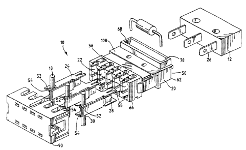
[0040] FIG. 7 depicts an exploded view of a second embodiment 200
of a connector incorporating different types of contacts 202, 204, 206 and a
housing
208 with cavities 210, 212, 214 formed therein. FIG. 7 shows the second
embodiment
9
CA 02402050 2002-09-10
200 in cooperation with an electrical assembly 14. The electrical assembly 14
includes a five position switch 216 having three (lower) terminals 218
integral with an
electrical device (lamp) 220 having two (upper) terminals 222. It should be
noted that
connectors of the invention can also function with other electrical assemblies
14 that
incorporate a different number of terminals, and switches having a different
number of
positions.
[0041] FIG. 8 shows a detailed view of a preferred contact design and
contact configuration of the second embodiment. Three different types of
contacts
202, 204, 206 are shown: upper contacts 202; lower terminal contacts 204; and
lower
circuit element contacts 206. The upper contacts 202 are configured to
cooperate with
the upper (lamp) terminals 222 of the electrical assembly 14 and with a
circuit
element 224. The lower terminal contacts 204 are configured to cooperate with
the
lower (switch) terminals 218 of the electrical assembly 14 and the external
conductors
226. The lower circuit element contacts 206 are configured to cooperate with
the
circuit elements 224 and the external conductors 226. Preferably, the lower
terminal
contacts 204 and lower circuit element contacts 206 define a lower cavity
plane
indicated at LCP, as shown in FIG. 9.
[0042] Each contact 202, 204, 206 has a design similar to contacts 24
of the first embodiment 10 described above. If desired, the contacts 202, 204,
206 can
be identical to one another and incorporate the design of contacts 24 of the
first
embodiment 10.
[0043] As shown in FIG. 8, each contact 202, 204, 206 preferably
includes first (top) and second (bottom) surfaces 228, 230 parallel to one
another, and
a third (lateral) surface 232 transverse, and preferably substantially
orthogonal, to the
first and second surfaces 228, 230.
[0044] The second embodiment includes at least one upper contact
202, at least one lower terminal contact 204, and at least one lower circuit
element
contacts 206. A first variation of the second embodiment (not shown) includes
two
upper contacts 202, two lower terminal contacts 204, and two lower circuit
element
contacts 206. In the first variation, at least one of the two upper terminals
222 of the
electrical assembly 14 is in electrical contact with an external conductor
226, and at
least one of the three lower terminals 218 of the electrical assembly 14 is in
electrical
CA 02402050 2002-09-10
contact with an external conductor 226. Specifically, at least one of the two
upper
contacts 202 is in electrical contact with at least one of the two lower
circuit element
contacts 206 by way of a circuit element 224. The at least one of the two
lower circuit
element contacts 206 is in electrical contact with an external conductor 226.
At least
one of the two lower terminal contacts 204 is in electrical contact with an
external
conductor 226.
[0045] A preferred contact configuration of the second embodiment
200 incorporating the three different types of contacts 202, 204, 206 is shown
in FIG.
8: ( 1 ) two upper contacts 202 include terminal receiving portions 234 and
circuit
element lead receiving portions 236 adjacent to one another and are located
substantially at a proximal end 238 of the upper contact; (2) three lower
terminal
contacts 204 include terminal receiving portions 240 and external conductor
receiving
portions 242 spaced from one another substantially at proximal 244 and distal
ends
246 of the lower terminal contacts 204; and (3) two lower circuit element
contacts 206
include circuit element receiving portions 248 and external conductor
receiving
portions 250 spaced from one another substantially at proximal 252 and distal
ends
254 of the lower circuit element contact 206.
[0046] In a preferred configuration, the terminal receiving portions
234, 240, external conductor receiving portions 242, 250, and circuit element
lead
receiving portions 236, 248 have a similar design and cooperate with the upper
and
lower terminals 222, 218, external conductors 226, and leads 256 of the
circuit
elements 224, respectively, as do the terminal receiving portions 28,
conductor
receiving portions 30, and circuit element lead receiving portions 74 of the
first
embodiment 10. It should be noted, however, that the contacts 202, 204, 206
and the
respective terminal receiving portions 234, 240, external conductor receiving
portions
242, 250, and circuit element lead receiving portions 236, 248 can be designed
and
configured differently, which different designs are within the scope and
spirit of the
present invention. Further, like the contact design of the first embodiment
10, the
external conductor receiving portions 242, 250 need not be spaced from the
terminal
receiving portions 242 or the circuit element lead receiving portions 248 of
the lower
terminal contacts 204 and lower circuit element contacts 206, respectively.
Likewise,
11
CA 02402050 2002-09-10
the circuit element lead portions 236 need not be adjacent the terminal
receiving
portions 234 of the upper contacts 202.
[0047] Preferably, as shown in FIG. 8, the upper contacts 202 and
lower circuit element contacts 206 are in electrical contact with one another
by way of
circuit elements 224. The circuit elements 224 can be, for example, a diode
258, a
connecting wire 260 or the like. The upper terminal 222, which cooperates with
the
terminal receiving portion 234 of the upper contact 202, can thus be in
electrical
contact with an external conductor 226 by way of the lower circuit element
contact
206, which includes its respective external conductor receiving portion 250.
Thus,
although both the upper and lower terminals 222, 218 of the electrical
assembly 14 are
in different planes, the external conductors 226 can be placed in electrical
contact with
the upper and lower terminals 222, 218 by connecting the external conductors
226 to
the external conductor receiving portions 242, 250 of the lower terminal
contacts 204
and lower circuit element contacts 206 in the lower cavity plane LCP. Such a
configuration reduces labor costs by allowing only one machine to connect the
external conductors 226 to the connector in one plane, as opposed to requiring
a more
elaborate machine or two machines to connect external conductors to the upper
and
lower terminals in two different planes.
[0048) As shown in FIG. 7, the housing 208 of the second embodiment
200 can include a top portion 262 that cooperates with a bottom portion 264 by
male
and female connectors 266, 268 formed on a top surface 296 of the bottom
housing
portion 264 and a bottom surface 270 of the top housing portion 262. The male
connector 266 can be a ledge 267 formed on the top surface 296 of the bottom
housing portion 264, and the female connector 268 can be a ledge receiving
structure
269 formed on the bottom surface 270 of the top housing portion 262. In other
embodiments not shown, the male connector 266 could be tabs depending from the
bottom surface 270 of the top housing portion 262, and the female connector
268
could be openings formed within the top surface 296 of the bottom housing
portion
264. Alternatively, the top portion 262 can be integral with the bottom
portion 264
(FIG. 8).
(0049] The top portion 262 includes at least one upper cavity 210, and
preferably, as shown in FIGS. 7 and 9, the top portion 262 includes two upper
cavities
12
CA 02402050 2002-09-10
210. The top portion 262 also includes two circuit element receiving recesses
272
that are configured to receive circuit elements 224. The two circuit element
receiving
recesses 272 are formed within a top surface 274 of the top housing portion
262. The
bottom portion 264 includes at least one lower terminal cavity 212 and at
least one
lower circuit element cavity 214. Preferably, as shown in FIG. 7, the bottom
portion
264 includes three lower terminal cavities 212 parallel with two lower circuit
element
cavities 214. Preferably, the lower terminal cavities 212 and lower circuit
element
cavities 214 define the lower cavity plane LCP shown in FIG. 9 one another so
that
the contacts 202, 204, 206 are not in electrical contact with one another.
(0050] Preferably, as shown in FIG. 7, the two upper cavities 210 each
include a terminal receiving portion 280 substantially at a proximal end 282
of the
upper cavities 210, and two circuit element lead apertures 284 formed within
each
circuit element receiving recess 272. It should be noted, however, that the
terminal
receiving portion 280 need not be substantially at the proximal end 282 of the
upper
cavities 210. The terminal receiving portions 280 of the upper cavities 210
are
configured to cooperate with the upper terminals 222 and the circuit element
lead
apertures 284 are configured to cooperate with the circuit element leads 256.
The
terminal receiving portions 280 and the circuit element lead apertures 284 can
cooperate with the upper terminals 222 and circuit element leads 256,
respectively, by
receiving them. The upper contacts 202 are positioned within the upper
cavities 210
so that their respective terminal receiving portions 234, 280 and circuit
element lead
portions 236 and apertures 284 are substantially aligned. Thus, when the
electrical
device 220 (light bulb in FIG. 6) is connected to the connector 200, the
terminal
receiving portions 280, 234 of the upper cavities 270 and contacts 202 receive
the
upper terminals 222 of the electrical assembly 14.
[0051] In the preferred embodiment of FIG. 7, the lower terminal
cavities 212 each include a terminal receiving portion 286 substantially at a
proximal
end 288 of the lower terminal cavities 212. The lower terminal cavities 212
also
include first and second external conductor openings 290, 292, substantially
at a distal
end 294, formed on top and bottom surfaces 296, 298 of the bottom housing
portion
264. It should be noted that the positioning of the terminal receiving portion
286 and
external conductor openings 290, 292 need not be at the proximal and distal
ends 288,
13
CA 02402050 2002-09-10
294 of the lower terminal cavities 212. Preferably, as shown in FIGS. 7 and 9,
the
lower terminal contacts 204 are positioned within the lower terminal cavities
212 so
that their respective terminal receiving portions 242, 286 are substantially
aligned
with one another and so that the external conductor receiving portions 242 and
the
first and second external conductor openings 290, 292 are substantially
aligned with
one another.
[0052] The preferred embodiment of FIG. 7 shows the lower circuit
element cavities 214 each including a circuit element lead receiving aperture
3.00
substantially at a proximal end 302 of the lower circuit element cavity 214.
The lower
circuit element cavities 214 also include first and second external conductor
openings
304, 306, at a distal end 308, formed at top and bottom surfaces 296, 298 of
the
bottom housing portion 264. It should be noted that the positioning of the
circuit
element lead receiving apertures 300 and external conductor openings 304, 306
need
not be at the proximal and distal ends 302, 308 of the lower circuit element
cavity
214. The lower circuit element contacts 206 of FIGS. 6 and 8 can be positioned
within the lower circuit element cavities 214 so that their respective circuit
element
lead receiving portions 248 and circuit element lead apertures 300 are
substantially
aligned, and so that their respective external conductor receiving portions
250 and first
and second external conductor openings 304, 306 are substantially aligned.
[0053] The second embodiment 200 can also include circuit elements
224 which can be positioned within the circuit element receiving recesses 272
of the
top housing portion 262. The top housing portion 262 can then be connected to
the
bottom housing portion 264 (if a two part housing is used). Each contact 202,
204,
206 can then be positioned into its respective cavity 210, 212, 214 so that
the circuit
element receiving portions 236, 248 of the upper contacts 202 and the lower
circuit
element contacts 206 cooperate with the circuit element leads 256. The upper
contacts 202 and lower circuit element contacts 206 would then be in
electrical
contact with one another via the circuit elements 226.
[0054] The housing-contact assembly (connector) 200 can be
connected to the electrical assembly 14 so that the upper and lower terminals
222, 218
are in electrical contact with the appropriate contacts 202, 204, 206. The
external
conductors 226 can then be connected to the external conductor receiving
portions
14
CA 02402050 2002-09-10
248, 242 of the lower circuit element contacts 206 and the lower terminal
contacts
204 so that they are received in the connector 200 transverse, and preferably
substantially orthogonal, to the lower cavity plane LCP. Thus, depending on
the
electrical circuit in which the connector is used, the lower terminals 218 of
the
electrical assembly 14 are connected to external conductors 226 via the lower
terminal
contacts 204, and the upper terminals 222 of the electrical assembly 14 are
connected
to the external conductors 226 via the upper terminal contacts 222, circuit
elements
224, and lower circuit element contacts 206.
[OOSSj As shown in FIGS. 7 and 9, the second embodiment 200 could
also include an end member 310 for cooperation with the distal end 312 of the
connector 200. The end member 310 includes at least two upper and at least two
lower apertures 314, 316. Preferably, as shown in FIGS. 7 and 9, the end
member 310
includes five upper and lower apertures 314, 316 formed on top and bottom
surfaces
318, 320 of the end member 310. Typically, the upper and lower apertures 314,
316
are of uniform size, but as shown in FIG. 9, one of the five upper and one of
the five
lower apertures 314, 316 can be elongated 317 to allow for cooperation with or
storage of two external conductors 226. To allow for cooperation with the two
external conductors, the external conductor receiving portion 242, 250 of the
respective lower terminal contact 204 or lower circuit element contact 206
would be
shaped accordingly to cooperate with two external conductors 226.
Alternatively, to
allow for storage of the two external conductors 226, there need not be any
respective
lower terminal contact 204 or lower circuit element contact 206.
[0056] In addition, the end member 310 can have a male connector 322
and the housing 208 can have a female connector (not shown) to allow the end
member 310 to cooperate with the housing 208. The male connector 322 of the
end
member 310 can be a ledge 324 depending from the top surface 318 of the end
member 310, arid the female connector (not shown) of the housing 208 can be a
ledge
(not shown) on a top surface 296 of the bottom housing portion 264. The
housing 208
and end member 310 can cooperate with one another so that the first and second
conductor openings 290, 292, 304, 306 of each lower terminal cavity 212 and
each
lower circuit element cavity 214 are substantially aligned with the five upper
and
lower apertures 314, 316 of the end member 310. If desired, a loose end 330 of
the
CA 02402050 2002-09-10
external conductors 226, extending from the lower apertures 316 of the end
member
310, can then be terminated.
[0057] From the foregoing it will be observed that numerous
modifications and variations can be effectuated without departing from the
true spirit
and scope of the novel concepts of the invention. It is to be understood that
no
limitation with respect to the specific embodiment illustrated is intended or
should be
inferred. The disclosure is intended to cover by the appended claims all such
modifications as fall within the scope of the claims.
16