Note: Descriptions are shown in the official language in which they were submitted.
CA 021402134 2004-12-08
1
OPTICALLY VARIABLE SECURITY DEVICE
The invention relates to an optically variable
security device for use, for example, for securing
documents and articles against counterfeiting.
The use of optical thin film structures to inhibit
counterfeiting and illicit tampering is now a well
established art. See for example US-A-3858977, US-A-
4721217,US-A-4930866,US-A-4994314, US-A-5009486, EP-A-
0733919 and Dobrowolski, J.A, Ho, F.C., and Waldorf, A.J.
"Research on Thin-Film Anticounterfeiting coatings at the
National Research Council of Canada," Applied Optics, Vol
28, No 14, pp 2702-2717, 1989. These thin film structures
often referred to as optical multilayers generally fall
into two types; those which are purely dielectric and those
which are composed of alternate dielectric (metal oxide or
polymer) and metallic layers. The former has the advantage
of being transparent and therefore suitable for over-
laminate applications, however it requires a minimum of
f ive layers to produce an iridescent device with acceptable
luminosity and colour saturation (seen to best effect when
located over a dark coloured substrate or background).
Whereas the metallic combination functions well with only
3 layers and is therefore significantly cheaper to
fabricate. However in both cases the iridescent quality of
the multi-layer is strongly influenced by the deposition
technology.
The optically variable effects produced by thin film
devices, although attractive and distinctive, are fairly
modest when compared to holograms and other diffraction
based optically variable devices (DOVID's). For a full
review of the various OVD technologies see "Optical
Document Security", chapter 11, editor R.L.van Renesse,
1997. Typically at a given viewing angle the observer will
see the device replay one colour or hue, while tilting the
device substantially within the plane of reflection will
CA 021402134 2004-12-08
2
either increase or decrease the optical path length
travelled by the light rays as they are reflected within
the layers thereby causing the device to undergo a colour
shift to a contrastingly different colour (in commercial
examples a typical shift is from blue-green to gold or red
to green) . Their appearance can be made more sophisticated
by incorporating into them graphical design elements like
logos and alphanumeric characters using techniques such as
masking (during the vacuum deposition stage) or laser
ablation to create voids within the layers, although these
substantially add to the fabrication cost of the device and
are limited in their scope. However in CA-A-2,172,113
where they teach the art of using UV or e-beam curable
acrylate monomer technology to fabricate metallic
reflection filters: various low cost non-vacuum methods are
described to produce patterned changes in the thickness of
the acrylate layer and therefore patterned areas of
relative colour shift with the background or hue of the
reflection filter. Though it should be said that a
consideration of these methods strongly infers that only
fairly coarse patterning is possible. In the case of
iridescent metallic reflection filters the technique of
producing demetallised shapes or indicia in the opaque
metal layer, using a chemical etchant has also been used to
produce more intricately patterned and therefore secure
OVD's.
The object of the invention is to design a new security
device which is more difficult to counterfeit than known
devices but yet relatively easy to inspect.
In accordance with a first aspect of the present
invention, there is provided an optically variable security
device comprising a thin film reflection filter structure
which exhibits a first optically variable effect; a relief
structure which exhibits a second optically variable effect,
the relief structure being provided on a layer separate from
and superposed on the thin film reflection filter structure;
CA 021402134 2004-12-08
2a
a decoupling layer between the relief structure layer and
the thin film reflection filter structure, the decoupling
layer being constructed such that a light ray impinging on
the side of the device nearest the relief structure layer is
directed into the observer's eye after being primarily
conditioned by only one of the relief structure and the thin
film reflection filter structure.
In accordance with a second aspect of the present
invention, a method of manufacturing an optically variable
security device comprises providing a relief structure on or
in a thin film reflection filter structure, the relief
structure and the thin film reflection film structure
CA 02402134 2002-09-04
WO 02/00445 PCT/GBO1/02902
3
exhibiting different first and second optically variable
effects .
We have devised a new security device which has a very
characteristic appearance, and by virtue of combining two
different technologies is inherently difficult to
counterfeit. In preferred examples, an iridescent
reflection filter based security device is patterned with
graphical elements/areas containing surface relief
structures often referred to in the art as an optical
microstructure, preferably a diffractive or holographic
microstructure - particularly as 1st order diffractive
iridescence has a very different appearance to that
produced by thin film interference (in the former, the
colour shifts are non-specular and evolve much more rapidly
with changes in viewing geometry). Also the diffractive
microstructure within the patterned areas can be originated
to exhibit clear kinegraphic or spatial movement effects on
tipping or rotating the device.
Now it should be appreciated that although thin film
iridescence and diffraction are both interference
phenomena, the former manifests this phenomena through
amplitude division whereas the latter depends on the effect
of wavefront division. This means the structures can be
combined in two fundamentally different ways . the first
way is to fabricate the security device such that the light
it directs into the observer s eye has been subject to (and
therefore conditioned by) both amplitude and wavefront
division (coupled system) or to fabricate the device such
that observed light has only been conditioned by either of
these effects acting separately (de-coupled system).
Consider Figure 1 which shows for simplicity a
transparent layer 1 sandwiched between a semi-transparent
metal layer 2 and an opaque metal layer 3. Typically, the
layer 2 is a partially transparent metal coating, the
middle layer 1 is a dielectric (metal oxide or polymer) and
the layer 3 an opaque metal coating (usually A1). When a
monochromatic beam of light 4 is incident upon the first
CA 02402134 2002-09-04
WO 02/00445 PCT/GBO1/02902
4
layer 2, its amplitude will be split or divided by partial
reflection: the reflected wave front will propagate
directly towards the observer whilst the second transmitted
beam will travel an optical path length of 2ndcos br,
where n is the refractive index of the layer 1 before
exiting the film and propagating towards the observer (it
will also experience a double absorption on twice passing
through the first metal layer 2). Clearly if the two
wavefronts (or partial amplitudes) travelling towards the
observer are to constructively interfere, thus enhancing
the reflectivity of the thin film system at that
1 wavelength, then the path difference between all
corresponding points on the two wavefronts must equal some
integer multiple, p, of the incident wavelength.
Now it can easily be shown that this optical path
difference (OPD ) is equal to 2nd cos fir; therefore assuming
there is the same reflective phase shift p at each
interface then the condition for constructive interference
is given by
p A =OPD=2ndcos Or
Conversely if the path difference OPD between the two
wavefronts is equal to an odd multiple of half wavelengths
(i.e. OPD =[ p +1/2 ]A ) then they will destructively
interfere -thus giving rise to reduced reflectance at that
wavelength.
If such a thin film structure is to effectively
function as an iridescent reflection filter then we
require two things: firstly that the effects of
constructive and destructive interfence are optimised to
achieve a high degree of luminosity and spectral
selectivity. Secondly the peak reflective wavelength (i.e.
the colour) of the thin film system should visibly change
as the observer changes the viewing geometry by a
convenient amount, i.e. it must exhibit clear colour shifts
when the plane of the device is tipped by around 10 degrees
within the plane of reflection (as defined by the light
CA 02402134 2002-09-04
WO 02/00445 PCT/GBO1/02902
source and observer). The first condition requires that
the amplitudes or intensities of the two reflected rays (5)
and (6) are as large as possible (maximizes constructive
interference) and ideally equal in amplitude so that they
5 cancel each other when 180 degrees out of phase (complete
destructive interference). Theoretically this requires
that the metals used for the semi-transparent and opaque
metal coatings 2,3 should have the highest inate/bulk
reflectivities. In particular a metal with a bulk
reflectivity approaching 100%, when deposited as a semi-
transparent coat ing ( i . a . between 5 - l2nm depending on metal
used) to create a specified partial reflection, will
minimise the loss of light due to absorption. Metals which
approach this ideal are Platinum, Palladium, Silver and
Aluminium - since the first three are generally in
commercial terms too costly this leaves aluminium as the
metal used in fabricating the reflective opaque layer.
However Aluminium is not chemically stable when deposited
at thicknesses less than l0nm tending to oxidise over time
- this constrains us to look at metals such as chromium,
Nickel and their alloys. Of these Chromium is the
preferred choice.
With regard to colour shift, i.e. the rate at which
the peak reflectance wavelength changes with observation
geometry, this is proportional to the optical path
difference and therefore the product nd - the larger this
value the more rapidly the colour of the reflection filter
changes with viewing angle. It should also be appreciated
that as the thickness increases from say 100nm onwards (and
assuming the refractive index of the dielectric layer to be
2.0), the device will initially function through first
order interference (p=1). However at around 180-200nm the
thin film structure supports both first order constructive
interference at the red end of the spectrum and second
order ( p=2 ) constructive interference at the blue end of
the spectrum. We then have created a device which exhibits
a red-orange to blue colour shift whereas a device
CA 021402134 2004-12-08
6
permitting only first order interference will only exhibit
continuous/gradual changes in colour, not a colour jump.
If we take this further, and increase the layer thickness
to around 350nm then the device will support both second
and third order interference producing a red to green
colour shift, which evolves more rapidly with angle than
the preceding case.
Having outlined the fundamental design and
manufacturing criteria for a metallic layer reflection
filter we next consider the physics of coupling this system
to a sinusoidal relief structure with a pitch of 1 um (see
Figure 2). Now the pitch of the relief structures that
compose a security hologram or DOVID are normally designed
or created such that the 1st order replay is approximately
at right angles to the plane of the device when illuminated
with white light 4. In practice this means holograms and
other DOVIDs contain grating structures with periodicities
ranging from 0 . 7 . ~.m to 1 . 4 . ~.m (hence the choice of 1 ~m for
inclusion in Figure 2). As regards the thickness d of the
intermediate layer we choose this on the basis of previous
discussion to be 0.2 um.
If we now consider rays incident at two different
points, A and B, on the first (partially metallised)
interface 2. At each point we see that, as before, a
fraction of the incident wavelet amplitude is directly
diffracted/reflected into the observer's eye. It should
be clear however from this scale drawing that this optical
path is very different for the two points of incidence on
the relief, i.e. the optical path at point A is twice that
at point B. It therefore follows that if at some
wavelength the partial amplitudes of the light ray
diffracted from the upper and lower interface at point A
are in phase, then those at point B may be near to being in
antiphase and therefore cancel out.
Although to simplify the argument we chose two points
of incidence on the relief profile that had markedly
different path lengths, it is clear that for the
CA 02402134 2002-09-04
WO 02/00445 PCT/GBO1/02902
7
periodicities that characterise most holograms or DOVTDs
(less than l.3um) the processes of diffraction (wavefront
division) and thin film interference (amplitude division)
will not in general couple efficiently together (i.e, the
processes of constructive and destructive interference can
never be optimised across all of the wavefront) leading to
reduced luminosity and spectral selectivity.
There will however be cases where it is desirable to
suppress certain colours in the diffraction spectrum of a
hologram/DOVID in which case the drawbacks of this coupled
system become secondary. Also this coupled system tends to
have the most direct fabrication routes : one route would be
to first emboss the holographic foil with holographic image
generating microstructure, preferably in defined or
selected areas. This microstructure is then vacuum coated
with first the semi-transparent metal coating, then the
dielectric layer, then the opaque metal layer, then
(optionally) a protective coating for increased chemical
durability and finally an adhesive coat.
However if the dielectric layer is composed of a UV
cured acrylate, then we can take advantage of the fact that
such a material is mechanically "non glassy" (i.e. ductile)
and therefore embossable. We therefore fabricate our
coupled device by, as before, first depositing a semi-
reflective metal coating onto the carrier foil which
depending on application may or may not be release coated.
We next deposit our u.v. or e-beam cured/polymerised
acrylate using the sequence of flash evaporation,
condensation and u.v./e-beam irradiation described in CA-A-
2,172,113 and then emboss the holographic generating
structure directly into the back surface of the reflection
filter (with the opaque metal coating, generally aluminium,
facing the embossing die or shim). Again a preferred
embodiment would be to confine the microstructure to a
pattern of selected areas such that the reflection is
decoratively patterned with holographic microstructure.
CA 02402134 2002-09-04
WO 02/00445 PCT/GBO1/02902
8
We propose here further developing the above
fabrication process by flash evaporating protective
acrylic layers either before the deposition of the first
semi-reflective metal coating or after the deposition of
the final opaque reflective metal coating or in some cases
both (though the former, acting as a protective overcoat is
particularly pertinent to the case where carrier foil is
simply a temporary substrate i.e. release layer present).
In either case the molecular composition of the acrylate
monomer can be adjusted to give the desired chemical or
mechanical durability.
Now it is known in the art (of vacuum coating science)
that achieving optimal adhesion between two coatings
requires that the structure remain under vacuum in between
the respective coating stages. We therefore propose a
refinement of the fabrication process in order to produce
a more tamper evident iridescent device. Specifically this
could be achieved in two ways: the simplest embodiment is
to admit air into the vacuum chamber (i.e "breaking the
vacuum") between the deposition of the first semi-
transparent metal coating and the deposition of the
dielectric layer or coating. Alternatively a molecular
species can be introduced into the vacuum which adsorbs on
to the surface of the first coating and then a second
coating is deposited. We thereby creating a weak interface
between the two coatings. Therefore in an attempt to
remove the security device from the article it is
protecting, this weak layer will fail before the adhesive
and in failing irreparably and obviously change the
appearance of the device.
Finally in relation to the coupled device we have
assumed that the opaque metal coating is continuous -
however we could modify the fabrication stage such that
this layer was spatially pattern metallised to create
transparent decorative shapes, meaningful forms of indicia
(e.g. letters, numbers) or a halftone pattern of
transparent dots. The fabrication of this discontinuous
CA 02402134 2002-09-04
WO 02/00445 PCT/GBO1/02902
9
metal coating could be effected in a number of ways: one
method would be to print an oil mask on to the dielectric
layer before vacuum coating the metal layer (the metal
would adhere only to the oil-free areas). A second method
would be to print an etchant directly onto the back of the
metal (in the case of aluminium, a suitable etchant would
be sodium hydroxide). Alternatively a third method would
be to print an etchant resistant mask on to back of the
aluminium before uniformly coating with etchant. Note in
methods two and three a final wash off stage will be
required to remove etchant and dissolved metal.
So fax we have proposed ways of fabricating coupled
devices which redirect into the observers eye only that
light which has been subject to the combined effect of the
two iridescence generating structures (e. g. surface relief
microstructure and thin film reflection filter). However
as we have alluded to earlier their may be many cases where
it is for example desirable to observe the full diffractive
rainbow spectrum of the holographic generating structure,
in which case we need to decouple the two iridescence
generating mechanisms. Herein we propose two distinct
approaches or arrangements for achieving this : in the first
arrangement, one or more opaque regions, typically achieved
through metallisation, may be provided between the
holographic image generating structure and the thin film
reflection filter structure. This provides a way of
shielding the relief structure from the thin film
reflection filter so that the holographic image can be
viewed, despite the presence of the thin film reflection
filter structure.
Advantage can be taken of the presence of the opaque
regions, to design them in predetermined shapes. In some
examples each region may define one or more of a crest,
logo, character or indicia, or a, preferably elongate,
shape through which moving patterns of diffractive light
progress.
CA 02402134 2002-09-04
WO 02/00445 PCT/GBO1/02902
In another arrangement, one or more layers/coatings
are provided between the holographic image generating
structure and the thin film reflection filter that are
substantially transparent. These would include one or more
5 high refractory layers (dielectric or semiconductor) and
one adhesive layer (preferably of high optical clarity) .
The refractory layer or layers should be composed (i.e.
have the relative refractive indices and coating
thicknesses) in such a way as to enhance the reflectivity
10 or luminosity of the holographic image generating
structure.
As with the opaque layers mentioned above, the
additional layers or coatings can be confined to only those
areas that contain holographic image generating structure
and typically may be in the form of crests, logos and the
like as mentioned above in connection with opaque layers.
So far we have made the assumption that the
diffractive microstructure supports devices that are viewed
in the first diffracted order. However, the above
fabrication methods could equally apply to zero order
diffraction devices (ZODs). These are devices in which the
periodicity of the relief is around 0.4~.m or less so that
for visible light no first order diffractive effects exist
at normal incidence illumination. The preferred shape of
the relief is rectangular and the depth of the relief is
ideally greater than or equal to the pitch. For a thorough
review of the characteristics of these devices and their
role in optical security, the reader is referred to Gale,
M.T., Knop, K.., and Morf, R., "Zero-order diffractive
microstructures for security applications" SPIE vo1.1210
Optical Security and Anticounterfeiting Systems, Los
Angeles 1990, pp83-89 and more recently in chapter 12 of
the publication "Optical Document Security' by R.L.van
Renesse. What is relevant to this discussion is that their
iridescence is superficially similar in appearance to
conventional reflection filters with one significant
CA 02402134 2002-09-04
WO 02/00445 PCT/GBO1/02902
11
difference, which is that their specular (i.e. zero order)
reflection is rotationally variable.
Specifically rotation of the microstructure in its
own plane leads to a major change in colour. For example,
when the grating grooves lie at right angles to the plane
of reflection (the normal viewing mode) the device may have
been designed to appear green. When, however, the ZOD is
rotated such that grooves lie in the plane of reflection
the device will appear brown in hue. We herein propose
combining this contrasting rotational behaviour between a
ZOD and a thin film interference reflection filter with our
general theme of confining the microstructure to selected
areas or regions that our superposed over the reflection
filter (e. g. patterning the reflection filter with
microstructure) to create a new security device, which both
in terms of optical variability and decorative effect, has
a differential appearance.
An example of one possible embodiment would be to
compose the device such that for one orientation, the ZOD
(microstructure grooves at right angles to the plane of
reflection) and the reflection filter have been designed to
reflect green/blue light and no decorative patterning will
be evident; however on rotation by 90 degrees the ZOD areas
will reveal themselves as a patterned areas of brown colour
shift on a green/blue background. In other examples the
patterning of the reflection filter with areas of ZOD
microstructure can be made more visually complex 'by
changing the orientation or pitch of the ZOD microstructure
from area to area. Indeed in a further refinement within
each of the selected areas the orientation/pitch of the ZOD
microstructure can be modified to create a zero-order image
within each area.
We have already discussed the limitation, that for
the 1 ,um grating periodicity typical of a hologram/DOVID,
multilayer enhancement is ineffective, degrading both the
thin film interference and diffractive effects. However,
at significantly longer periodicities such as 3 /.cm or more
CA 02402134 2002-09-04
WO 02/00445 PCT/GBO1/02902
12
it can be shown graphically that every point on the
wavefront travels a near equal (double pass) optical path
length within the film. In other words a reflection filter
will function efficiently when applied or conforming to
relief structures with a periodicity ~ 3 ,um. Now if these
relief structure are fabricated to be triangular profiles,
and if they have a periodicity of 5 ,um or more, then they
will start to exhibit refractive/reflective characteristics
as well as diffractive i.e. they will function as
lenticular microprisms or micromirrors. We therefore
propose directly embossing decoratively and securely
patterned areas of this relief structure into a
metal/polymer reflection filter - although direct
deposition could also be use for "glassy, non-embossable
dielectrics".
It should be appreciated that the effect of
impressing the think film structure with the profile of
these coarse microprisms/micromirros will be to locally
change the specular normal and therefore colour replayed by
the thin film structure. We would therefore have a
security device consisting of an iridescent reflection
filter which at one orientation will be decoratively
patterned with areas of a different iridescent hue or
colour) prism grooves perpendicular to axis of reflection) .
When the observer rotates the device by 90 degrees these
patterned areas will progressively transform into the same
colour as the background (prism/grooves along axis of
reflection) .
It is well known that the random surface relief
created by holographically recording the speckle
irradiances pattern generated by a suitable diffusing
screen, will in turn, when embossed into metallised foil
produce reflective diffuser with a whitish hue.
In another example, therefore, we provide a device in
which an iridescent reflection filter is decoratively and
intricately patterned (e. g. with logos, text, microtext
etc.) with areas of random diffuse microstructure. This
CA 02402134 2002-09-04
WO 02/00445 PCT/GBO1/02902
13
can be most simply achieved by directly embossing into a
metal/polymer thin film system. The random microstructure
will substantially suppress the specular iridescence
created by the thin film structure and ideally replace it
with one, which has a distinctive whitish hue.
The security device can be used on a wide variety of
documents and articles including visas, passports,
licences, cheques, identity cards, plastic cards, bank
notes, tickets, bonds, share certificates, vouchers,
passes, permits, electrostatic photocopies electrostatic
laser printed materials, brand authentication labels,
serial numbering slips, quality control certificates, bills
of lading and other shipping documentation, legal documents
and tamper evident labels . Tt can also be used in embedded
features such as security threads.
Some examples of security devices and methods
according to the invention will now be described with
reference to the accompanying drawings, in which:-
Figures 1 and 2 are schematic, cross-sections through
devices to show the problems of combining thin film
reflection filters with surface relief holographic image
generating structures;
Figure 3 is a plan of an example of a security device
according to the invention;
Figures 4A, 4B, 5A, 5B and 5C are schematic cross-
sections through first to fifth examples of decoupled
security devices according to the invention; and,
Figures 6 to 8 are schematic cross-sections through
sixth to eighth examples of coupled security devices
according to the invention.
The appearance of a typical decoupled device is shown
in Figure 3 in which the diffractive microstructure
(holographic imagery) 10-12 is confined to patterned areas
or domains that are opaquely metallised - the reflection
filter acting as an iridescent background. Although not
visible in Figure 3, the background will exhibit different
CA 02402134 2002-09-04
WO 02/00445 PCT/GBO1/02902
14
colours in the regions 13,14, the colours gradually merging
when they meet.
These areas or domains 10-12 will have shapes which
are aesthetically relevant to holographic imagery contained
within them - they may be crests, logos, characters or
elongated shapes through which moving patterns of
diffracted light could progress.
This decoupled device could be fabricated in several
ways depending on the proposed application and composition
of the reflection filter. The first way (Figure 4A) would
be to first emboss the patterned areas of holographic
imagery 20 into a l-5~m thick lacquer layer 21 of a
holographic foil 26. The foil 26 also comprises a carrier
25, typically 12-25/.cm thick polyester (PET), and a wax or
silicone release layer 21A, typically 0.01-0.1/~m thick.
An opaque metal coating 22A, for example 20-50nm
thick Al is then coated or applied to one or more selected
regions, preferably in register with the microstructure 20,
as shown. This can be achieved either by directly printing
an oil mask prior to the metal coating or by applying the
metal coating and the selectively demetallising.
Next a semi-reflective coating 22, such as Cr, Ni or
alloys such as Ni-chrome, 5-12/.cm thick is applied.
The complete area of the foil (on the microstructure
side) is then successively coated, layer after layer to
build up the desired thin film system 23. The dielectric
layers may be metal oxides with thicknesses in the range
0.1-l~.m (preferably 0.2-0.5~.m) or acrylates (embossable)
typically these are created by flash evaporation of the
monomer acrylate, followed by condensation onto the foil,
followed by e-beam or W curing. Suitable molecular
weights for the monomer lie in the range 150-600 but
especially 200-300. Thicknesses as for dielectrics. An
example of a particular acrylate composition would be:
Lauryl Monoacrylate 48.5% pbw
Tricyclic hydrocarbon diacrylate 48.5% pbw
CA 02402134 2002-09-04
WO 02/00445 PCT/GBO1/02902
Adhesion Promoters 30.0% pbw
A fully reflective opaque metal layer 24 such as 30-
50nm thick A1 is then coated on the dielectric layer 23.
5 A hot melt or pressure sensitive adhesive layer 27 is then
coated on the layer 24 to a typical thickness of 0.5-20~.m.
The materials and thicknesses mentioned above are
also applicable to the examples to be described below where
the same reference numerals are used to identify similar
10 layers.
Figure 4B illustrates a modified form of the Figure
4A example in which the embossed lacquer layer is omitted,
and the microstructure is embossed directly into the
carrier 25A without an intermediate release layer. In this
15 case, the carrier layer 25A is transparent to enable the
device to be observed after it has been transferred on to
a substrate. The carrier 25A may be I2-25 micron thick
polyester but could also be polypropylene or PVC, with
thicknesses in the range 10-60~tm. This structure is
suitable for labels (with a pressure sensitive adhesive 27)
or for threads with an optional heat activated adhesive.
The remaining layers are provided in a similar manner to
Figure 4A. However, an optional protective back coat could
be provided between layers 24 and 27, particularly if the
device will be used in a thread. This could be another UV
curable acrylate provided in the same coating run as .the
layer 24.
The second approach would be to take a prefabricated
thin film system and coat it with an embossable lacquer and
then repeat the above sequence of patterned embossing and
demetallisation. Next, the embossed lacquer is coated with
a protective varnish (e. g. UV curing) and then finally
laminated to a release coating Barrier film (i.e.
polyester) and adhesive coat.
The third approach would be simply to take the
demetallised/pattern metallised embossed film (release
coated carrier included if required) such as a therformable
CA 02402134 2002-09-04
WO 02/00445 PCT/GBO1/02902
16
foil and laminate to it (using an optically clear adhesive)
the prefabricated thin film system. For the layer 23A, the
monomer deposited acrylate layers described in CA-270113
are suitable.
In a further example, a therformable foil is embossed
with the desired surface relief microstructure coated with
one or more refractory (substantially transparent) layers,
which may or may not be in register with the surface relief
regions and then laminated to a thin film reflection filter
structure.
In the examples described above, an opaque metal
layer 22A is provided between the microstructure and the
thin film reflection structure 23. Figure 5a illustrates
an example of a decoupled system. A holographic foil 26 is
embossed as in Figure 4A. In this case, the foil is
provided with an additional protective coating 34 (which
could also be used in Figure 4A) . This provides mechanical
and chemical durability and is typically 1-5,um thick. Next
one or more reflective enhancing dielectric layers (only
one shown in Figure 5A) is applied. These layers could be
coated in a spatially continuous manner over the entire
area of the foil - or using masking techniques they could
be applied/deposited over only the areas containing the
holographic imaging or microstructure. A clear laminating
adhesive layer 31 is coated onto the HRI layer 30,
following which this structure is laminated to a previously
fabricated reflection filter comprising a transparent, thin
metal layer 32 of for example Cr or Ni, a thin film
reflection filter layer 23, and an. opaque metal layer 24.
If required, an adhesive 27 is then applied. If desired,
the HRI layer 30 can be confined to one or more regions
between the microstructure 20 and the thin film reflection
filter structure 23.
Figure 5B illustrates a modification of the Figure 5A
example, in which the microstructure 20 is embossed
directly into the carrier 25B. In this case, the carrier
CA 02402134 2002-09-04
WO 02/00445 PCT/GBO1/02902
17
26 will not be removed from the device when it is
transferred onto a substrate,
Figure 5C illustrates another modification of Figure
5A in which the layer 30 is replaced by a discontinuous
metal layer 50. In the preferred example, the layer 50 is
30-50% demetallized. As can be seen, the layer 50 is
registered with the microstructure 20 as well as having
non-registered portions.
The examples described above are all decoupled
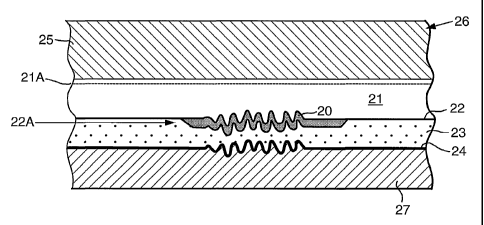
systems. Figure 6 illustrates a first example of a coupled
system. In this example, a holographic foil 26 comprising
a carrier 25 and release layer 21A, for example a hot
stamping f oil or a cold transfer foil, is used, and a
protective coating 34, ideally composed of UV durable
acrylate monomer is applied. Next a semi-reflective metal
coating 22 is provided on the layer 34, the coating, as
before, typically comprising 5-l2nm thick chrome, Ni or
alloy.
A dielectric layer 23 is applied, this being a
suitable UV curable acrylate monomer and then the
dielectric layer 23 is coated with an opaque fully
reflective metal layer 24, such as aluminium, having a
thickness in the range of 30-50nm. This structure is then
embossed with a surface relief microstructure 20 and
finally an optional, adhesive coating 27 is applied, such
as a hot melt or pressure sensitive adhesive.
Figure 7 is similar to the structure of Figure 6,
except that the release layer 21A and protective layer 34
are omitted, so that the carrier 25 will form part of the
finished device. Further, the adhesive layer 27 is
replaced by a protective coating 40, such as W curable
acrylate. This structure is suitable for use as a thread.
Finally, Figure 8 illustrates a structure based on
the Figure 6 example, and in which the layer 24 is
patterned to match the microstructure regions 20.