Note: Descriptions are shown in the official language in which they were submitted.
CA 02402196 2002-09-06
WO 01/67609 PCT/USO1/07243
HIGH SPEED LOGIC FAMILY
BACKGROUND OF THE INVENTION
The present invention generally relates to digital logic families, and more
particularly, to digital logic families for high speed circuits.
Moore's Law, which is named after the founder of Intel Corporation, Gordon
Moore, states that the speed and density of computers will double every 18-24
months.
For the most part, Moore's Law has held true since the early days of the
microprocessor,
and is predicted to do so for at least another twenty years.
A corollary to Moore's Law is that the size of the transistors used in
integrated
1 o circuits must shrink by a factor of two every 18-24 months. Until
recently, this was
accomplished by simply scaling bulls MOSFET devices. However, as the
transistor
channel lengths scale below about 0.25um, a number of transistor effects begin
to
degrade the transistor's characteristics. Some of these effects include short-
channel
effects, gate resistance effects, chasanel profiling effects and other
effects. It has been
found that reducing the power supply voltage can reduce some of these effects,
but the
performance of the resulting circuit also tends to suffer.
A number of logic families have been proposed for producing higher
performance circuits, some of which use pass-transistor logic. Pass-transistor
logic
families often can implement a desired logic function using fewer transistors
than
2o conventional CMOS logic. One common pass-transistor logic family is lcnown
as
Complementary Pass-transistor Logic (CPL), and is discussed in U.S. Patent No.
5,808,483 to Salvo and in "A 1.5-ns 32-b CMOS ALU in Double Pass-Transistor
Logic"
by Suzulci et al. A typical CPL logic gate uses only NMOS transistors to
produce
relatively low input capacitances and relatively high performance circuits.
A limitation of many pass-transistor logic families, including CPL is that the
high output signal level tends to be lower than the supply voltage by an NMOS
threshold voltage. This reduces the noise margin of the circuit, and in turn,
the speed of
the circuit. The usual way to avoid this is to use CMOS Pass-Transistor Logic,
where
full-swing operation is achieved by adding PMOS transistors in parallel with
the NMOS
3o transistors of a CPL gate. This, however, produces higher input capacitance
and slower
circuit performance.
-1-
CA 02402196 2002-09-06
WO 01/67609 PCT/USO1/07243
Another pass-transistor logic family is called Dual Pass-Transistor Logic
(DPL).
Dual Pass-Transistor Logic (DPL) is a modified version of CPL, and is often
used for
reduced supply voltage applications. Unlike CPL, DPL uses both NMOS and PMOS
pass-transistors. A typical DPL OR/NOR gate is shown in Figure 1, with the NOR
gate
shown at 100 and the OR gate shown at 102. Both the NOR gate 100 and the OR
gate
102 use complimentary input signals A, A , B and B .
Fox the NOR gate 100, input A is coupled to the gate terminals of NMOS
transistor 104 and PMOS transistor 106. PMOS transistor 106 has a source that
is
coupled to a power supply voltage (VDD) 107, and a drain that is coupled to an
output
to terminal 112. NMOS transistor 104 has a source that is coupled to the input
B , and a
drain that is coupled to the output terminal 112.
Tiiput B is coupled to the gate terminals of NMOS transistor 108 and PMOS
transistor 110. PMOS transistor 110 has a source that is coupled to the power
supply
voltage (VDD) 107, and a drain that is coupled to the output terminal 112.
NMOS
transistor 108 has a source that is coupled to input A , and a drain that is
coupled to the
output terminal 112.
For the OR gate I02, input A is coupled to the gate terminals of NMOS
transistor 120 and PMOS transistor I22. NMOS transistor I20 has a source that
is
coupled to ground 123, and a drain that is coupled to output terminal 124.
PMOS
2o transistor 122 has a source that is coupled to the input B, and a drain
that is coupled to
the output terminal 124.
Input B is coupled to the gate terminals of NMOS transistor 126 and PMOS
transistor 128. NMOS transistor 126 has a source that is coupled to ground
123, and a
drain that is coupled to the output terminal 124. PMOS transistor 128 has a
source that
is coupled to input A, and a drain that is coupled to the output terminal 124.
Dual Pass-Transistor Logic (DPL) can produce higher circuit performance than
CPL because dual current paths are available for driving the output of the
gate. For
example, for the NOR gate 100 shown in Figure l, when inputs A and B are both
low,
PMOS transistor 106 and PMOS transistor 110 are both "on". Thus, PMOS
transistor
106 provides a first current path for pulling the output terminal 112 high,
and PMOS
-2-
CA 02402196 2002-09-06
WO 01/67609 PCT/USO1/07243
transistor 110 provides a second current path for pulling the output terminal
112 high.
When input A is low and input B is high, PMOS transistor 106 is "on", and
NMOS transistor 108 is "on" with the drain pulled lugh (i.e., input A is
high).
Accordingly, PMOS transistor 106 provides a first current path for pulling
output 112
high, and NMOS transistor 108 provides a second current path for pulling the
output
terminal 112 high.
When input A is high and input B is low, PMOS transistor 110 is "on", and
NMOS transistor 104 is "on" with the drain pulled high (i.e., input B is
high).
Accordingly, PMOS traxlsistor 110 provides a first current path for pulling
output
to terminal 112 high, and NMOS transistor 104 provides a second current path
for pulling
output terminal 112 high.
Finally, when input A and input B are both high, NMOS transistor 104 is "on"
and NMOS transistor 108 is "on", both with their drains pulled low (i.e., both
A and B
are low). As such, NMOS transistor 104 provides a first current path for
pulling the
output terminal 112 low, and NMOS transistor 108 provides a second current
path for
pulling the output terminal 112 low.
The dual current paths provided by DPL are thought to increase the performance
of DPL relative to CPL. In addition, the dual current paths are thought to
allow rail-to-
rail switching, which may increase the noise margin and performance of DPL
relative to
2o CPL, especially under reduced power supply conditions.
SUMMARY OF THE INVENTION
The present invention provides a logic family that produces the same
advantages
as DPL, but uses fewer transistors and provides increased performance relative
to DPL.
This is preferably accomplished by removing one or more of the transistors
from DPL.
It has been found that not all of the transistors in DPL may be required, and
in many
cases, some of the transistors reduce the performance and density of the gate.
This
observation is counter to the general understanding of DPL logic gates,
because the
removal of one or more of the transistors from a DPL gate may eliminate one or
more of
the dual current paths discussed above. It is the dual current paths that were
thought to
3o be beneficial for increasing the performance of DPL. It has been
discovered, however,
-3-
CA 02402196 2002-09-06
WO 01/67609 PCT/USO1/07243
that a DPL gate may not operate as a collection of independent pass
transistors. Rather,
it appears there is an interaction between the pass-transistors that produces
gain, much
lilce a CMOS gate. Thus, it has also been found that if selected transistors
are removed
from a typical DPL gate, the gate can still provide the desired logic
function, but at
higher speeds and with higher densities.
Tn a first illustrative embodiment of the present invention, a two-input logic
circuit is provided. The illustrative two-input logic circuit includes a first
transistor, a
second transistor, and a third transistor. The first transistor and second
transistor have a
first polarity, and the third transistor has a second polarity. The source of
the first
to transistor is coupled to a power supply voltage, the drain of the first
transistor is coupled
to the output of the logic circuit, and the gate of the first transistor is
coupled to a first
input signal. The source of the second transistor is coupled to the power
supply voltage,
the drain of the second transistor is coupled to the output of the logic
circuit, and the
gate of the second transistor is coupled to a second input signal. Finally,
the source of
the third transistor is coupled to a third input signal, the drain of the
third transistor is
coupled to the output of the Iogic circuit, and the gate of the third
transistor is coupled to
the first input signal. Preferably, the third input signal is the compliment
of the second
input signal.
Unlike a conventional two-input DPL gate, the logic circuit does not have a
2o fourth transistor, where the source of the fourth transistor is coupled to
the compliment
of the first input signal, the drain of the fourth transistor is coupled to
the output of the
logic circuit, and the gate of the fourth transistor is coupled to the second
input signal.
As such, the present invention uses fewer transistors than conventional DPL
gates.
For a two-input NAND gate (A NAND B), the first transistor and second
transistor are P-type transistors (e.g., PMOS), the third transistor is an N-
type transistor
(e.g., NMOS), and the power supply voltage is VDD (e.g., 3.3V). The first
input signal,
which is provided to the gate of the first transistor (P-type), may correspond
to the B
input. The second input signal, which is provided to the gate of the second
transistor (P-
type) and to the gate of the third transistor (N-type), may correspond to the
A input. The
3o third input signal, which is provided to the source of the third transistor
(N-type), may
correspond to the compliment of the B input, or B .
-4-
CA 02402196 2002-09-06
WO 01/67609 PCT/USO1/07243
Fox a two-input OR gate (A OR B), the polarity of the input signals may be
simply reversed relative to the two-input NAND gate discussed above. For
example,
the first input signal, which is provided to the gate of the first transistor
(P-type), may
correspond to the compliment of the B input, or B . The second input signal,
which is
provided to the gate of the second transistor (P-type) and to the gate of the
third
transistor (N-type), may correspond to the compliment of the A input, or A .
The third
input signal, which is provided to the source of the third transistor (N-
type), may
correspond to the B input.
For a two-input NOR gate, (A NOR B), the first transistor and second
transistor
1o are N-type transistors (e.g., NMOS), the third transistor is a P-type
transistor (e.g.,
PMOS), and the power supply voltage is ground. The first input signal, which
is
provided to the gate of the first transistor (N-type), may correspond to the B
input. The
second input signal, which is provided to the gate of the second transistor (N-
type) and
to the gate of the third transistor (P-type), rnay correspond to the A input.
The third
is input signal, which is provided to the source of the third transistor (P-
type), may
correspond to the compliment of the B input, or B' .
For a two-input AND gate (A AND B), the polarity of the input signals may be
simply reversed relative to the two-input NOR gate discussed above. That is,
the first
input signal, which is provided to the gate of the first transistor (N-type),
may
2o correspond to the compliment of the B input, or B . The second input
signal, which is
provided to the gate of the second transistor (N-type) and to the gate of the
third
transistor (P-type), may correspond to the compliment of the A input, or A .
The third
input signal, which is provided to the source of the third transistor (P-
type), may
correspond to the B input.
25 In some embodiments, the third transistor may be coupled to the third input
signal through one or more other transistors, preferably of the second
polarity type. For
example, for a three-input NAND gate, the source of the third transistor may
be coupled
to the drain of a fourth transistor, with the source of the fourth transistor
coupled to the
third input signal. The gate of the fourth transistor may then be coupled to a
fourth
30 input signal, such as a C input. To complete the three-input NAND gate, a
fifth
-5-
CA 02402196 2002-09-06
WO 01/67609 PCT/USO1/07243
transistor may be provided, with the gate of the fifth transistor coupled to
the C input,
the source of the fifth transistor coupled to the power supply voltage, and
the drain of
the fifth transistor coupled to the output of the gate.
The above-described logic circuits are only illustrative. With the
accompanying
disclosure, one skilled in the art could derive numerous other logic functions
to form a
logic family.
-6-
CA 02402196 2002-09-06
WO 01/67609 PCT/USO1/07243
BRIEF DESCRIPTION OF THE DRAWINGS
Other objects of the present invention and many of the attendant advantages of
the present invention will be readily appreciated as the same becomes better
understood
by reference to the following detailed description when considered in
connection with
the accompanying drawings, in which like reference numerals designate like
parts
throughout the figures thereof and wherein:
Figure 1 is a schematic diagram of a prior art DPL two-input AND/NAND gate;
Figure 2 is a schematic diagram of an illustrative two-input AND/NAND gate in
accordance with the present invention;
1o Figure 3 is a schematic diagram of an illustrative two-input OR/NOR gate in
accordance with the present invention;
Figure 4 is a schematic diagram of an illustrative three-input AND/NAND gate
in accordance with the present invention;
Figure 5 is a graph showing illustrative output signals for each stage of a
series
string of pass-transistor logic gates; and
Figure 6 is a graph showing illustrative output signals for each stage of a
series
string of logic gates constructed in accordance with the present invention.
DETAILED DESCRIPTION OF THE PREFERRED EMBODIMENTS
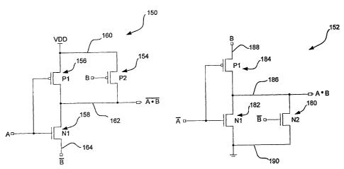
Figure 2 is a schematic diagram of an illustrative two-input AND/NAND gate in
2o accordance with the present invention. The two-input NAND gate is shown
generally at
150 and the two-input AND gate is generally shown at 152. The two-input NAND
gate
150 includes two input signals A and B, along with the compliment B of the B
input
signal. Thus, the illustrative the two-input NAND 150 gate actually has three
input
signals.
A first transistor 154 and a second transistor 156 are P-type transistors
(e.g.,
PMOS), and a third transistor 158 is an N-type transistor (e.g., NMOS). The
gate of the
first transistor (P-type) 154 is coupled to input signal B, the source of the
first transistor
(P-type) I54 is coupled to the power supply voltage (VDD) 160, and the drain
of the
first transistor (P-type) 154 is coupled to the output 162 of the gate. The
gate of the
3o second transistor (P-type) 156 is coupled to input signal A, the source of
the second
transistor (P-type) 156 is coupled to the power supply voltage (VDD) 160, and
the drain
CA 02402196 2002-09-06
WO 01/67609 PCT/USO1/07243
of the second transistor (P-type) 156 is coupled to the output 162 of the
gate. Finally,
the gate of the third transistor (N-type) 158 is coupled to input signal A,
the source 164
of the third transistor (N-type) 158 is coupled to the compliment B of the
first input
signal, and the drain of the third transistor (N-type) 158 is coupled to the
output 162 of
the gate, as shown.
Unlike the conventional two-input DPL NAND gate 100 shown in Figure 1, the
illustrative two-input NAND gate does not include NMOS transistor 108 of
Figure 1.
Accordingly, the illustrative two-input NAND gate may provide the same logic
function
as the DPL NAND gate 100 shown in Figure 1, but with fewer transistors.
Simulations
1o have shown that the illustrative two-input NAND gate of the present
invention may not
only occupy less physical space, but may also operate at higher speeds while
still
providing gain.
When both inputs A and B axe low, the first transistor (P-type) 154 and the
second transistor (P-type) 156 are "on", and the third transistor (N-type) 158
is "off'.
I5 As such, the first transistor (P-type) 154 and the second transistor (P-
type) 156 pulls the
output 162 of the NAND gate high.
When input A is low and input B is high, the first transistor (P-type) 154 is
"off', the second transistor (P-type) 156 is "on", and the third transistor (N-
type) 158 is
"off'. As such, the second transistor (P-type) 156 pulls the output 162 of the
NAND
2o gate high.
When input A is high and input B is low, the first transistor (P-type) 154 is
"on",
the second traxlsistor (P-type) 156 is "off', and the third transistor (N-
type) 158 is "on".
As such, the first transistor (P-type) 154 pulls the output 162 of the NAND
gate high. Tn
addition, however, the source 164 of the third transistor (N-type) 158 is high
because it
25 is coupled to the compliment B of input B. Accordingly, the third
transistor (N-type)
158 helps pull the output 162 of the NAND gate high.
Finally, when input A is high and input B is high, the first transistor (P-
type) 154
is "off', the second transistor (P-type) 156 is "off', and the third
transistor (N-type) 158
is "on". The source 164 of the third transistor (N-type) 158 is low because it
is coupled
3o to the compliment B of input B. As such, the third transistor (N-type) 158
pulls the
_g_
CA 02402196 2002-09-06
WO 01/67609 PCT/USO1/07243
output 162 of the NAND gate low. It has been found that the illustrative two-
input
NAND gate is faster than the conventional DPL two-input NAND gate shown in
Figure
1.
Referring now to the two-input AND gate 152 of Figure 2. The two-input AND
gate 152 includes two compliment input signals A and B , along with the input
signal
B. As such, the illustrative the two-input AND gate 152 actually has three
input signals
A , B and B.
A first transistor 180 and a second transistor 182 are N-type transistors
(e.g.,
PMOS), and a third transistor 184 is a P-type transistor (e.g., PMOS). The
gate of the
to first transistor (N-type) 180 is coupled to input signal B , the source of
the first
transistor (N-type) 180 is coupled to the power supply voltage (GND) 190, and
the drain
of the first transistor (N-type) 180 is coupled to the output 186 of the gate.
The gate of
the second transistor (N-type) 182 is coupled to input signal A , the source
of the second
transistor (N-type) 182 is coupled to the power supply voltage (GND) 190, and
the drain
of the second transistor (N-type) 182 is coupled to the output 186 of the
gate. Finally,
the gate of the third transistor (P-type) 184 is coupled to input signal A ,
the source 188
of the third transistor (P-type) 184 is coupled to the input signal B, and the
drain of the
third transistor (P-type) 184 is coupled to the output 186 of the gate.
Again, unlike the conventional two-input DPL AND gate 102 shown in Figure l,
2o the illustrative two-input AND gate does not include PMOS transistor 128 of
Figure 1.
Accordingly, the illustrative two-input AND gate may provide the same Iogic
function
as the DPL AND gate 102 shown in Figure 1, but with fewer transistors.
Simulations
have shown that the illustrative two-input AND gate of the present invention
not only
may occupy less physical space, but may also operate at higher speeds while
still
providing gain.
When both inputs A and B are low ( A and B are high), the first transistor (N-
type) I80 and the second transistor (N-type) 182 are "on", and the third
transistor (P-
type) 184 is "off'. As such, the first transistor (N-type) 180 and the second
transistor
(N-type) 182 pull the output 186 of the AND gate low.
-9-
CA 02402196 2002-09-06
WO 01/67609 PCT/USO1/07243
When input A is Iow and input B is high ( A is high and B is low), the first
transistor (N-type) 180 is "off', the second transistor (N-type) 182 is "on",
and the third
transistor (P-type) 184 is "off'. As such, the second transistor (N-type) 182
pulls the
output 186 of the AND gate Iow.
When input A is high and input B is low ( A is low and B is high), the first
transistor (N-type) 180 is "on", the second transistor (N-type) 182 is "off',
and the third
transistor (P-type) 184 is "on". As such, the fixst transistor (N-type) 180
pulls the output
186 of the AND gate low. In addition, the source 188 of the third transistor
(P-type)
184 is low because it is coupled to B, which is the compliment B wluch is
high.
to Accordingly, the third transistor (P-type) 184 also helps pull the output
186 of the AND
gate low.
Finally, when input A is high and input B is high ( A is low and B is low),
the
first transistor (N-type) 180 is "off', the second transistor (N-type) 182 is
"off', and the
third transistor (P-type) 184 is "on". The source 188 of the third transistor
(P-type) 184
is now high, because it is coupled to B, which is the compliment B which is
low. As
such, the third transistor (P-type) 184 pulls the output 186 of the AND gate
high. It has
been found that the illustrative two-input AND gate is faster than the
conventional DPL
two-input AND gate showwn in Figure 1.
Figure 3 is a schematic diagram of an illustrative two-input OR/NOR gate in
2o accordance with the present invention. The two-input NOR gate is shown
generally at
200 and the two-input OR gate is generally shown at 202. The two-input NOR
gate 200
includes two input signals A and B, along with the compliment B of the B input
signal.
The two-input OR gate 202 includes two input signals A and B , along with the
input
signal B. Accordingly, each of the illustrative two-input NOR gate 200 and two-
input
OR gate 202 actually have three input signals.
The illustrative two-input NOR gate 200 is identical to the two-input AND gate
described above with reference to Figure 2 except the polarity of the input
signals are
reversed. That is, the input signal A is provided to the gates of the second
transistor (N-
type) 182 and the third transistor (P-type) 184. Lilcewise, the input signal B
is provided
3o to the gate of the first transistor (N-type) 180. Finally, the compliment
of the input
-10-
CA 02402196 2002-09-06
WO 01/67609 PCT/USO1/07243
signal B ( B ) is provided to the souxce of the third transistor (P-type) 184.
This
arrangement provides the NOR (A NOR B) function.
The illustrative two-input OR gate 202 is identical to the two-input NAND gate
described above with reference to Figure 2 except the polarity of the input
signals are
reversed. That is, the compliment of the input A ( A ) is provided to the
gates of the
second transistor (P-type) 156 and the third transistor (N-type) 158.
Likewise, the
compliment of the input B (B ) is provided to the gate of the first transistor
(P-type)
154. Finally, the input signal B is provided to the source of the third
transistor (N-type)
158. This arrangement provides the OR (A OR B) function.
1 o Figure 4 is a schematic diagram of an illustrative three-input AND/NAND
gate
in accordance with the present invention. The three-input NAND gate is shown
generally at 210, and includes three input signals A, B and C, along with the
compliment C of the C input signal. Thus, the illustrative the three-input
NAND gate
210 actually has four input signals.
A first transistor 212, a second transistor 214, and a third transistor 216
are P-
type transistors (e.g., PMOS), and a fourth transistor 218 and a fifth
transistor 220 are
N-type transistors (e.g., NMOS). The gate of the first transistor (P-type) 212
is coupled
to input signal C, the source of the first transistor (P-type) 212 is coupled
to the power
supply voltage (VDD) 222, and the drain of the first transistor (P-type) 212
is coupled to
2o the output 224 of the gate. The gate of the second transistor (P-type) 214
is coupled to
input signal B, the source of the second transistor (P-type) 214 is coupled to
the power
supply voltage (VDD) 222, and the drain of the second transistor (P-type) 214
is
coupled to the output 224 of the gate. The gate of the third transistor (P-
type) 216 is
coupled to input signal A, the source of the third transistor (P-type) 216 is
coupled to the
power supply voltage (VDD) 222, and the drain of the third transistor (P-type)
216 is
coupled to the output 224 of the gate.
The gate of the fourth transistor (N-type) 218 is coupled to input signal B,
and
the drain of the fourth transistor (N-type) 218 is coupled to the output 224
of the gate.
Finally, the gate of the fifth transistor (N-type) 220 is coupled to input
signal A, the
3o source 228 of the fifth transistor (N-type) 220 is coupled to the
compliment C of the
-11-
CA 02402196 2002-09-06
WO 01/67609 PCT/USO1/07243
input signal C, and the drain of the fifth transistor (N-type) 220 is coupled
to the source
230 of the fourth transistor (N-type) 218, as shown.
As in Figure 2, it is contemplated that a separate three-input AND gate may be
provided to generate an AND output. However, in the embodiment shown, an
inverter
234 is coupled to the output 224 of the NAND gate. This produces an overall
NAND/AND function that has fewer transistors than the approach shown in Figure
2.
However, the inverter 234 introduces an extra gate delay when producing the
AND
output 240. The particular approach used will depend on the desired
application.
The above-described logic circuits are only meant to be illustrative. With the
1o accompanying disclosure, one skilled in the art can derive numerous other
logic
functions, including storage elements, to form a logic family. °
Figure 5 is a graph showing illustrative output signals for each stage of a
series
string of pass-transistor logic gates, such as CPL gates. Complimentary input
signals I
250 and I 252 are provided to the input terminals of a first stage in the
string of pass-
transistor logic gates. The complimentary outputs O1 and Ol of the first stage
are
shown at 254 and 256, respectively. These complimentary outputs Ol 254 and Ol
256
are provided to the input terminals of a second stage in the string of pass-
transistor Iogic
gates.
The complimentary outputs OZ and OZ of the second stage are shown at 258
2o and 260, respectively. These complimentary outputs OZ 258 and OZ 260 are
provided
to the input terminals of a third stage in the string of pass-transistor logic
gates. The
complimentary outputs 03 and 03 of the third stage are shown at 262 and 264,
respectively. These complimentary outputs 03 262 and 03 264 are provided to
the
input terminals of a fourth stage in the string of pass-transistor Iogic
gates.
The complimentary outputs Oø and 04 of the fourth stage are shown at 266 and
268, respectively. These complimentary outputs 04 266 and Oø 268 are provided
to
the input terminals of a fifth stage in the string of pass-transistor logic
gates. The
complimentary outputs OS and OS of the fifth stage are shown at 270 and 272,
respectively. These complimentary outputs OS 270 and OS 272 are provided to
the
-12-
CA 02402196 2002-09-06
WO 01/67609 PCT/USO1/07243
input terminals of a sixth stage in the string of pass-transistor logic gates.
Finally, the
complimentary outputs 06 and 06 of the sixth stage are shown at 274 and 276,
respectively.
As can be seen, the output signals produced by each stage of the gates tend to
become successively more degraded. Both the slope and amplitude of the output
signals
are reduced, which can impact the performance and noise margins of the
circuit. The
degradation in the output signals illustrates the lack of gain produced by
each pass-
transistor logic gate. To overcome this limitation, amplifier stages are
commonly
inserted at various locations in the delay path. This, however, decreases both
the
l0 performance and density of the circuit.
Figure 6 is a graph showing illustrative output signals for each stage of a
series
string of AND/NAND gates constructed in accordance with Figure 2 above.
Complimentary input signals I 350 and I 352 axe provided to the input
terminals of a
first stage in the string of gates. The complimentary outputs O1 and Ol of the
first
stage are shown at 354 and 356, respectively. These complimentary outputs O1
354
and Ol 356 are provided to the input terminals of a second stage in the string
of gates.
The complimentary outputs Oz and Oz of the second stage are shown at 358
and 360, respectively. These complimentary outputs Oz 358 and OZ 360 axe
provided
to the input terminals of a third stage in the string of gates. The
complimentary outputs
2o O3 and O3 of the third stage are shown at 362 and 364, respectively. These
complimentary outputs 03 362 and 03 364 axe provided to the input terminals of
a
fourth stage in the string of gates.
The complimentary outputs OQ and 04 of the fourth stage are shown at 366 and
368, respectively. These complimentary outputs 04 366 and Oø 368 are provided
to
the input terminals of a fifth stage in the string of gates. The complimentary
outputs OS
and OS of the fifth stage are shown at 370 and 372, respectively. These
complimentary
outputs OS 370 and OS 372 are provided to the input terminals of a sixth stage
in the
string of gates. Finally, the complimentary outputs 06 acid 06 of the sixth
stage are
-13-
CA 02402196 2002-09-06
WO 01/67609 PCT/USO1/07243
shown at 374 and 376, respectively.
As can be seen, the output signals produced by each stage of the string of
gates
of the present invention do not become significantly degraded. Both the slope
and
amplitude of the various output signals tend to remain relatively constant.
This
indicates that the logic gates of the present invention produce gain, much
like a CMOS
gate. Accordingly, logic gates constructed in accordance with the present
invention may
have increased performance and increased noise margins relative the standard
pass-
transistor logic families such as CPL. In addition, and because the logic
gates of the
present invention have fewer transistors than standard CMOS gates, the logic
gates of
to the present invention may have increased performance and increased density
relative to
standard CMOS gates.
Having thus described the preferred embodiments of the present invention,
those
of skill in the art will readily appreciate that the teachings found herein
may be applied
to yet other embodiments within the scope of the claims hereto attached.
-14-