Note: Descriptions are shown in the official language in which they were submitted.
CA 02402229 2002-08-30
WO 01/67512 PCT/USO1/07410
-1-
METHOD AND APPARATUS FOR DELIVERING
POWER TO HIGH PERFORMANCE ELECTRONIC ASSEMBLIES
CROSS-REFERENCE TO RELATED APPLICATIONS
This application claims benefit of the following U.S. Provisional Patent
Applications, each of which are incorporated by reference herein:
Application Serial No. 60/187,777, entitled "NEXT GENERATION
PACKAGING FOR EMI CONTAINMENT, POWER DELIVERY, AND THERMAL
DISSIPATION USING INTER-CIRCUIT ENCAPSULATED PACKAGING
TECHNOLOGY," by Joseph T. DiBene II and David H. Hartlce, filed March 8, 2000;
Application Serial No. 60/196,059, entitled "EMI FRAME WITH POWER
FEED-THROUGHS AND THERMAL INTERFACE MATERIAL IN AN
AGGREGATE DIAMOND MIXTURE," by Joseph T. DiBene II and David H.
Hartke, filed April 10, 2000;
Application Serial No. 60/219,813, entitled "HIGH CURRENT
MICROPROCESSOR POWER DELIVERY SYSTEMS," by Joseph T. DiBene II,
filed July 21, 2000;
Application Serial No. 60/232,971, entitled "INTEGRATED POWER
DISTRIBUTION AND SEMICONDUCTOR PACKAGE," by Joseph T. DiBene II
and James J. Hjerpe, filed September 14, 2000;
Application Serial No. 60/251,222, entitled "INTEGRATED POWER
DELIVERY WITH FLEX CIRCUIT INTERCONNECTION FOR HIGH DENSITY
POWER CIRCUITS FOR INTEGRATED CIRCUITS AND SYSTEMS," by Joseph
T. DiBene II and David H. Hartke, filed December 4, 2000;
Application Serial No. 60/251,223, entitled "MICRO-I-PAK FOR POWER
DELIVERY TO MICROELECTRONICS," by Joseph T. DiBene II and Carl E. Hoge,
filed December 4, 2000; and
Application Serial No. 60/251,184, entitled "MICROPROCESSOR
INTEGRATED PACKAGING," by Joseph T. DiBene II, filed December 4, 2000.
CA 02402229 2002-08-30
WO 01/67512 PCT/USO1/07410
-2-
This patent application is also continuation-in-part of the following co-
pending
and commonly assigned patent applications, each of which applications are
hereby
incorporated by reference herein:
Application Serial No. 09/353,428, entitled "INTER-CIRCUIT
ENCAPSULATED PACKAGING," by Joseph T. DiBene II and David H. Hartke,
filed July 15, 1999;
Application Serial No. 09/432,878, entitled "INTER-CIRCUIT
ENCAPSULATED PACKAGING FOR POWER DELIVERY," by Joseph T. DiBene
II and David H. Hartke, filed November 2, 1999;
Application Serial No. 09/727,016, entitled "EMI CONTAINMENT USING
INTER-CIRCUIT ENCAPSULATED PACKAGING TECHNOLOGY" by Joseph T.
DiBene II and David Hartlce, filed November 28, 2000;
Application Serial No. --/---,---, entitled "METHOD AND APPARATUS FOR
PROVIDING POWER TO A MICROPROCESSOR WITH INTEGRATED
THERMAL AND EMI MANAGEMENT," by Joseph T. DiBene II, David H. Hartke,
James J. Hjerpe Kaskade, and Carl E. Hoge, filed February 16, 2001; and
Application Serial No. --/---,---, entitled "THERMALIMECHANICAL
SPRINGBEAM MECHANISM FOR HEAT TRANSFER FROM HEAT SOURCE
TO HEAT DISSIPATING DEVICE," by Joseph T. DiBene II, David H. Hartke,
Wendell C. Johnson, and Edward J. Derian, filed March 2, 2001.
This patent application is also related to Application Serial No. --/---,---,
entitled "METHOD AND APPARATUS FOR THERMAL AND MECHANICAL
MANAGEMENT OF A POWER REGULATOR MODULE AND
MICROPROCESSOR IN CONTACT WITH A THERMALLY CONDUCTING
PLATE," by Joseph T. DiBene II and David H. Hartlce, filed on same date
herewith,
which application is hereby incorporated by reference herein.
CA 02402229 2002-08-30
WO 01/67512 PCT/USO1/07410
-3-
BACKGROUND OF THE INVENTION
1. Field of the Invention
This invention relates in general to a system for providing electrical
continuity
between a plurality of circuit boards, and in particular to a method and
apparatus for
improving the packaging and distribution of power to high performance
electronic
circuit assemblies.
2. Description of the Related Art
As electronic circuitry becomes more complex, paclcaging of the circuitry has
become more difficult. The common method for packaging integrated circuits
(ICs)
and other electronic components is to mount them on printed circuit boards
(PCBs) or
other substrates such as ceramics having alternating conductive and non-
conductive
layers or planes sandwiched or bonded together to form a dense X-Y signal
interconnect. For a number of years, the operating voltage of ICs was
approximately 5
volts and the power consumption was generally less than 1 watt. This
relatively high
supply voltage and low power level allowed the packaging of a large number of
ICs
on a single PCB with power distribution incorporated into one or more of the
PCB
planes.
More recently advances in silicon fabrication techniques have permitted the
manufacture of high performance IC packages with operating voltages at or
below 1
volt and power levels in excess of 100 watts. As described in co-pending and
commonly assigned patent application serial number --/---,---, METHOD AND
APPARATUS FOR PROVIDING POWER TO A MICROPROCESSOR WITH
INTEGRATED THERMAL AND EMI MANAGEMENT, by Joseph T. DiBene II,
David H. Hartke, James J. Hjerpe Kaskade, and Carl E. Hoge, filed February 16,
2001, which application is hereby incorporated by reference, the transient
current to
some of these packages can exceed hundreds of amps per microsecond. To assure
optimum performance under these conditions, it is important that the
electrical path
from the power supply to the IC be designed to accommodate high current flow
and
low series inductance, two goals which are difficult to achieve at the same
time. The
CA 02402229 2002-08-30
WO 01/67512 PCT/USO1/07410
-4-
present invention achieves both of these goals, while also allowing for a
compact,
integrated stack-up system design that permits thermal dissipation and control
of
electromagnetic interference (EMI).
SUMMARY OF THE INVENTION
To address the requirements described above, the present invention discloses a
method, apparatus, article of manufacture, for providing power from a first
circuit
board having a first circuit board first conductive surface and a first
circuit board
second conductive surface to a second circuit board having a second circuit
board first
conductive surface and a second circuit board second conductive surface. The
apparatus comprises a first conductive member, includiilg a first end having a
first
conductive member surface electrically coupleable to the first circuit board
first
conductive surface and a second end distal from the first end having a first
conductive
member second surface electrically coupleable to the second circuit board
first
surface. The apparatus also comprises a second conductive member, having a
second
conductive member first surface electrically coupleable to the first circuit
board
second surface and a second conductive member second surface distal from the
second conductive member first surface electrically coupleable to the second
circuit
board second conductive surface. In one embodiment of the invention, the
second
conductive member is hollow, and is disposed within the second conductive
member
in a coaxial arrangement. If desired, a dielectric can be placed between the
first
conductive member and the second conductive member. The dielectric, or the
dimensions of the first conductive member and the second conductive member can
be
defined so that the apparatus exhibits an impedance that can be used
cooperatively
with circuit elements on either the first circuit board or the second circuit
board. One
of the advantages of the present invention is the integration of function in
which the
apparatus operates both as a rigid standoff to separate the first circuit
board from the
second circuit board, and a conduit for delivering power and a ground return
(or other
signals) between the circuit boards as well. While the apparatus will be
discussed in
terms of providing a power signal from a first circuit board to a second
circuit board,
CA 02402229 2002-08-30
WO 01/67512 PCT/USO1/07410
-5-
it can also be used to provide power to a plurality of circuit boards in a
stacked up
configuration, all with minimal impedance.
BRIEF DESCRIPTION OF THE DRAWINGS
Referring now to the drawings in which like reference numbers represent
corresponding parts throughout:
FIG. 1A is a two-dimensional section view illustrating an architecture in
which the present invention may be usefully employed in delivering power to a
microprocessor;
FIG. 1B is a section view of a microprocessor package used in FIG. 1A which
further illustrates the location of the power standoff assemblies associated
with
delivering power to the microprocessor shown if FIG. 1A;
FIG. 2A is a two-dimensional section view of a conceptual coaxial
interconnect illustrating the delivery of electrical energy from an upper
planar circuit
structure to a lower planar circuit structure;
FIG. 2B is two-dimensional plan view of the current flow to the coaxial
interconnect structure in the upper planar circuit of FIG. 2A;
FIG. 3 is a two-dimensional section view of a power standoff assembly
structure in which the imler cylinder is swaged to the upper planar circuit
and a screw
forms both a mechanical and electrical coimection to a lower planar circuit;
FIG. 4 is a two-dimensional section view of a power standoff assembly
structure in which the inner cylinder is swaged to the upper planar circuit
and a
crushable spring washer forms an electrical connection from the inner cylinder
to a
lower planar circuit while a screw forms the mechanical connection;
FIG. 5 is a two-dimensional section view of a power standoff assembly
structure in which the inner cylinder is swaged to the upper planar circuit
and a screw
forms the mechanical connection of the inner cylinder to the lower circuit
structure
while a spring feature is incorporated into the outer cylinder in order to
accommodate
electrical connection of the outer cylinder to the lower planar circuit;
CA 02402229 2002-08-30
WO 01/67512 PCT/USO1/07410
-6-
FIG. 6 is a two-dimensional section view of a power standoff assembly
structure in which the inner cylinder is swaged to the upper planar circuit
and a screw
forms the mechanical connection of the inner cylinder to the lower circuit
structure
while a spring insert is incorporated into the outer cylinder in order to
accommodate
electrical connection of the outer cylinder to the lower planar circuit;
FIG. 7A is a two-dimensional section view of a power standoff assembly
structure in which the inner and outer cylinders are soldered to the upper
planar circuit
while the connection of these cylinders to the lower planar circuit is
accommodated by
the use of a coaxial spring contact assembly;
FIG. 7B is a two-dimensional plan section view of the power standoff
assembly structure of FIG. 7A further illustrating the coaxial spring contact
assembly;
FIG. 8A is a two-dimensional section view of a power standoff assembly
structure in which coaxial ring structures are joined to both the upper and
lower planar
circuit to form coaxial blades which engages into spring furrows which are Ian
integral
part of the inner and outer cylinders of the power standoff assembly;
FIG. 8B is a two-dimensional plan view of the coaxial ring structure of FIG.
8A;
FIG. 8C is a two-dimensional plan view looping into the spring furrows of the
inner and outer cylinders of FIG. 8A;
FIG. 9A is a two-dimensional section view of a planar circuit structure
illustrating how the layers in a mufti-layered circuit structure can be
arranged to
efficiently couple dynamic electrical current impulses from the inner planes
of the
planar structure to the inner and outer cylinders of a coaxial power standoff
assembly
utilizing a screw connection as illustrated in FIG. 3;
FIG. 9B is a two-dimensional plan view of the top most layer of FIG. 9A;
FIG. 9C is a two-dimensional plan view of the upper inner layer of FIG. 9A;
FIG. 9D is a two-dimensional plan view of the lower inner layer of FIG. 9A;
and
FIG. 9E is a two-dimensional plan view of the lower most layer of FIG. 9A;
CA 02402229 2002-08-30
WO 01/67512 PCT/USO1/07410
FIG. 10 is a 2-dimensional plan view of a power standoff assembly structure
which is surrounded with capacitors in order to improve the overall connection
impedance;
FIG. 1 1A is a 2-dimensional side view of an EMI frame using power standoff
assemblies integral with the frame assembly;
FIG. 11B is a 2-dimensional plan section view of the EMI frame shown in
FIG. 10A; and
FIG. 12 is a diagram illustrating how the power standoff assembly can be used
as a circuit element between the circuit boards.
DETATLED DESCRIPTION OF PREFERRED EMBODIMENTS
In the following description, reference is made to the accompanying drawings
which form a part hereof, and which is shown, by way of illustration, several
embodiments of the present invention. It is understood that other embodiments
may
be utilized and structural changes may be made without departing from the
scope of
the present invention.
Overview
The present invention discloses an apparatus for providing power from a first
circuit board to a second circuit board. In one embodiment, the apparatus
(hereinafter
alternatively referred to as a POWERDIRECT or a standoff) comprises an inner
cylindrical cylinder, an intermediate coaxially located insulator or
dielectric material
and an outer coaxially located cylindrical cylinder. The standoff is disposed
between
a first planar structure or printed circuit board and a second planar
structure or printed
circuit board to provide a path for the transfer of electrical power and a
ground return
between the two planar structures in an efficient manner. This creates a very
low
impedance interconnect between power and groundplanes on the first planar
structure
and power and ground planes on the second planar structure.
The present invention discloses a variety of methods in which the coaxial
cylinders of the power standoff assembly may be joined to the upper and lower
planax
CA 02402229 2002-08-30
WO 01/67512 PCT/USO1/07410
_g_
structures and their internal power planes. It also discloses efficient
methods of
connecting the internal power planes of the planar structures to external land
features
of the planar structures in such a manner as to further enhance the efficacy
of the
interconnect between power planes on the first planar structure and power
planes on
the second planar structure.
The present invention further describes a specific application where the power
standoff assembly may be especially beneficial to delivering power to high
performance microprocessor packages in such a manner as to negate the need to
integrate power regulation circuitry directly onto the microprocessor package
(On-
Paclcage-Voltage-Regulation, OPVR) so as to improve the producibility, yield
and
cost of modern high performance microprocessors.
Encapsulated Circuit Assembly
Typically, a modern high performance microprocessor die is flip-chip attached
to an organic or ceramic substrate utilizing a Controlled-Collapse-Chip-
Connection
(C4). The substrate has one or more power planes which are used to distribute
power
to the chip connections. Often the power requirements of the microprocessor
exceed
100 watts at operating voltages of approximately 1 volt and transient current
requirements in excess of 100 amps per microsecond. Typically power
conditioning
may be provided by a voltage regulation module (VRM). The stringent power
demands require that the VRM be very closely coupled to the microprocessor or
directly mounted on to the microprocessor substrate. OPVR architectures
combine
VRM technology with high performance silicon technology all on a common
substrate. The OVPR often very expensive because of the very large number of
layers
required to manage both the power and signal interconnect to the
microprocessor die.
The resulting assembly also has reduced yield and higher costs than what might
be
achieved if the microprocessor function could be separated from the VRM
function.
FIG. 1A is a diagram illustrating a stack up assembly 100 illustrating the use
of a power standoff assembly 105 to deliver power to a microprocessor
substrate 101
and its associated lid 108 from a remotely located VRM assembly 102. In the
CA 02402229 2002-08-30
WO 01/67512 PCT/USO1/07410
-9-
illustrated embodiment, the VRM assembly 102 surrounds the microprocessor lid
108,
thus saving space in the z (vertical) axis.
The microprocessor lid 108 is thermally coupled to a heatsink structure 106
through a thermal coupling mesa 107 and appropriate thermal interface material
S (TIM) such as thermal grease (not shown) which can be integral to the base
of 107 or
a separate structure that is coupled (i.e. bonded, or metallically fused) to
the base of
the heatsink structure 106. Furthermore, heat generated from components in the
VRM
assembly 102 can be thermally attached directly to the base of heatsink
assembly 106,
thus sharing the heat dissipation benefits of the heatsink assembly 106.
Signals from
the microprocessor can be comlected through pins (not shown) to soclcet 104
which is
mounted to main board 103.
Power front the VRM assembly 102 is efficiently coupled to the
microprocessor substrate 101 by utilizing one or more power standoff
assemblies 10S.
In one embodiment, four power standoff assemblies l OS are used, and each is
located
1 S proximate a corner of the microprocessor substrate 101.
FIG. 1B is a diagram showing the location of the four power standoff
assemblies l OS proximate the corners of the microprocessor substrate l OS.
The power
standoff assemblies l OS may be located in other locations on the substrate
101 such as
at the center of each side. Further, the number of power standoff assemblies l
OS used
can be varied to meet the power needs of target microprocessor or other high
performance Integrated Circuit assembly.
Coaxial Interconnect
FIGs. 2A and 2B are diagrams illustrating transfer of energy from a source
2S (such as a VRM assembly 102) on a first circuit board 201 to a second
circuit board
202 through one or more power standoff assemblies 105.
A power signal 211 supplying current flows from the VRM on the first circuit
board 201 (hereinafter alternatively referred to as first PCB) through a
conductive
plane 204 in or on the first circuit board 201 to one or more power standoff
assembly
connections 10SD. The power signal 211 then passes through the first
conductive
CA 02402229 2002-08-30
WO 01/67512 PCT/USO1/07410
-10-
member l OSA to similar connections on the second circuit board 202 and then
onto a
conductive plane 207 in or on the second circuit board 202, and thence to the
load
(e.g. the IC, microprocessor or other power dissipating device). A ground
return
signal 212 passes from a ground plane 206 in or on the second circuit board
202
through a conductive surface 213 to a second conductive member l OSB, through
the
second conductive member lOSB, to a conductive plane 205 on or in the first
circuit
board 201. This acts as a ground return for the VRM power signal 211. The
space
between the first conductive member lOSA and the second conductive member lOSB
may include a dielectric or electric insulator lOSC, if desired.
In a preferred embodiment, the second conductive member l OSB is hollow and
the first conductive member 105A is disposed within the second conductive
member
lOSB such that they are substantially coaxial (e.g. the major axis of the
first
conductive member and the major axis of the second conductive member are co-
linear). In this embodiment, the series inductance of the power standoff
assembly 105
is governed primarily by the basic equation;
ooh
Lcoar - 2~ ln(D° l DI )
where ,tt~ is the permeability of space, h is the length of the power standoff
1 OS body,
Do is the inner diameter of the outer conductor, and DI is the diameter of the
inner
conductor. As the diameters get closer to each other the natural log function
approaches zero. This is the theoretical limit the inductance may achieve with
such a
construction. Practical issues limit achieving this limit however with such a
construction the actual inductance achieved may be very low.
As described further with respect to FIGS. 9A-9E, the power plane 204, 206
and the ground plane 205, 207 of the first circuit board 201 and the second
circuit
board 202 may be on inner layers, instead of on an external surface of the
circuit
boards 201, 202. In this case, through holes can be used on the first circuit
board 201
and second circuit board 202. These thru-hole patterns can also be coaxially
arranged
proximate to where first and second conductive members l OSA, l OSB are
connected
CA 02402229 2002-08-30
WO 01/67512 PCT/USO1/07410
-11-
to the first and the second circuit boards 201, 202. Also, plane inductance
(inductance
from the plane pairs 204/205 and 206/207) can be reduced by the bringing the
plane
pairs 204/205 and 206/207 closer together.
One of the reasons for reducing the interconnection inductance is that the
voltage drop across the interconnect is crucial for proper operation. As
stated
previously, high current slew-rates can create large drops across an inductive
interconnect. This may be seen by the simple equation for the dynamic voltage
drop
across an interconnect:
_ _d1
1 O ~ ~ = I STEPRAC + I'TOT dt
Where Is~e~ is the step current the IC creates when switching transistors
internally, RAE
is the AC resistance of the interconnect, LTOT 1S the total inductance of the
interconnect, and dlldt is the rate of change or AC current slew-rate which
occurs due
to the switching transistors. Often the inductance is the dominant element in
the path
and thus contributes to the largest portion of the drop across the
interconnect.
Coaxial and Multi-Axial Embodiments
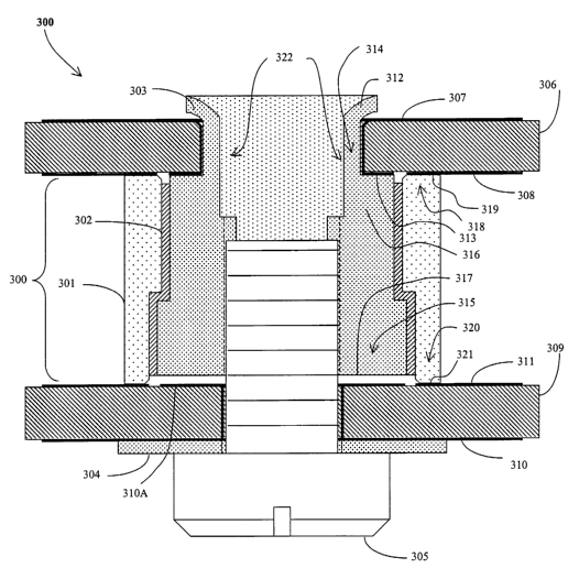
FIG. 3 is a diagram illustrating a preferred embodiment of a power feed
standoff assembly 300. The power feed standoff assembly 300 is used to route
power
and/or signals from a first circuit board 306 to a second circuit board 309.
The power feed standoff assembly 300 comprises a first conductive member
303 and a second conductive member 301. In the illustrated embodiment, the
second
conductive member 301 is hollow, and the first conductive member 303 is
disposed
within the second conductive member 301. Also, the first conductive member 303
and second conductive member 301 are coaxial (e.g. the longitudinal axes of
symmetry of each are substantially colinear). Hence, the first conductive
member
303 is disposed within and coaxially with the second conductive member 301.
The first conductive member 303 includes a first end 314. The first end 314
includes a shoulder portion 316 having a first conductive member first surface
313
CA 02402229 2002-08-30
WO 01/67512 PCT/USO1/07410
-12-
that is electrically coupleable to a first conductive surface 307 on the first
circuit
board 306, such as a pad. The first conductive member 303 also includes a
second
end 315 distal from the first end 314 having a first conductive member second
surface
317 electrically coupleable with a first conductive surface 310 or pad of the
second
circuit board 309. In the illustrated embodiment, the first conductive member
second
surface 317 does not directly contact the first surface 310A of the second
circuit board
309. Instead, electrical coupling between the first conductive member second
surface
317 and the first suxface 310 of the second circuit board 309 is accomplished
by a
screw 305 that is electrically coupled to both the first conductive member 303
and the
first surface 310 of the second circuit board. As can be seen from FIG. 3,
direct
contact between the second end 315 of the first conductive member and the
first
surface 310 of the second circuit board 309, (e.g. between first conductive
member
second surface 317 and surface 310A) is possible as well.
The second conductive member 301 includes a first end 318 having a second
conductive member first surface 319. The second conductive member first
surface
319 is electrically coupled to a first circuit board 306 second conductive
surface 308.
In the illustrated embodiment, the second conductive member first surface 319
is
directly coupled to the first circuit board 306 second conductive surface 308,
but this
need not be the case.
The second conductive member 301 includes a second end 320 having a
second conductive member second surface 321. The second conductive member
second surface 321 is electrically coupled to the second circuit board second
surface
311. In the illustrated embodiment, the second conductive member second
surface
321 is directly coupled to the second circuit board second surface 311, but
this need
not be the case.
In the illustrated embodiment, both the first conductive member 303 and the
second conductive member 301 are cylindrical in shape (e.g. generally circular
in
cross section), but this need not be the case. Although the circular cross
section
depicted is preferred, the first and second conductive members 303, 301 may be
of an
ovoid, rectangular, or trapezoidal cross section. Or, the conductive members
301, 301
CA 02402229 2002-08-30
WO 01/67512 PCT/USO1/07410
-13-
may simply be a pair of adjacent linear conductive members having an insulator
or
insulating space therebetween. In each case, the longitudinal axes of symmetry
for the
first and second conductive members 301, 303 can be made substantially co-
linear.
The first conductive member 303 is also disposed through a plated through
hole (PTH) in the first circuit board 306. The inner conductive member 303 can
be
affixed to the first circuit board 306 by a swage 312. The swage 312 works
cooperatively with the shelf portion 316 to affix the first conductive member
303 to
the first circuit board 306.
The inner conductive member 303 can be further attached to the first circuit
board 306 by soldering. However, soldering alone is not the preferred method
of
affixing the first conductive member 303 to the first circuit board 306.
The plated through hole 322 and the surrounding first circuit board first
surface 307 together with the first conductive member 303 define an inner
coaxial
power circuit. In one embodiment, the inner coaxial power circuit is completed
by a
conductive fastening device 305 such as a screw, which makes electrical
contact with
the first conductive member 303 and the second circuit board first surface
310, thus
forming an electrically conductive path from the first circuit board 306 to
the second
circuit board 309. In one embodiment, the inner conductive member 303 includes
hollow portion having a threaded inner surface configured to accept and hold.
Also,
the height of the first conductive member 303 is typically slightly less than
the height
of the second conductive member 301 for the reasons described below.
The second conductive member 301 forms the outer coaxial circuit engaging
the first circuit board second surface 308 (which may include a power pad
pattern) and
the second circuit board second surface 311. In one embodiment, dielectric 302
does
not grip the first conductive member 303 and the second conductive member 310
so
tightly that their relative position can not be adjusted slightly with a force
imparted by
fastener 305 such that the upper surface 313 of outer conductor 305 can come
into
intimate contact with the first circuit board second surface 308, thus
completing the
upper half of the outer coaxial power circuit.
CA 02402229 2002-08-30
WO 01/67512 PCT/USO1/07410
-14-
Because the inner conductor 303 is slightly shorter than outer conductor 301
both circuit feeds have identical and predictable joining forces between PCB
306 and
PCB 309. Such would not be the case if the two conductors 303, 30I were of
approximately equal length where slight variations in length may cause an
unpredictable shift in forces between the two conductors as they press against
the
surfaces of PCB 306 and 309. Further, the fact that the first conductive
member 303
and the second conductive member 301 are coaxially arranged to reduce the
unwanted
electromagnetic fields that might be created from electric disturbances
induced into
the assembly 300.
Production
The power feed standoff assembly 300 may be produced by separately
fabricating items 301, 302 and 303 and pressing them together forming an
inseparable
assembly. The power feed standoff assembly 300 may also be produced by
separately fashioning the inner conductive member 303 and the outer conductive
member 301, supporting the members 301, 303 in a fixture, and inserting a
dielectric
302 into the gap separating 301 and 303 (e.g. under heat and pressure) and
curing the
dielectric material 302.
It should be noted that outer conductor 301, dielectric 302 and inner
conductor 303
can be separate parts that are assembled in a different sequence than is
described
above without detracting from the benefits of this invention.
Further Embodiments
FIG. 4 is a two-dimensional sectional view of another embodiment of the
power feed standoff assembly 300. This embodiment is similar to that which is
depicted in FIG. 3, however, a compressible conductive member such as a
crushable
washer 401 is disposed between the second circuit board 309 first surface 310
and the
second conductive member second surface 317. This provides a direct path by
which
current in the first conductive member 303 passes directly to the first
conductive
surface 310 on the second circuit board 309. Crushable washer 401
significantly
CA 02402229 2002-08-30
WO 01/67512 PCT/USO1/07410
-15-
reduces the inductance of the electrical interconnect because current does not
have to
proceed through the screw body to the second circuit board 309 first
conductive
surface 310 but rather can proceed directly from the base of first conductive
member
303 to the second circuit board 309 first conductive surface 310. The
crushable
washer 401 still provides the benefits of providing predictable forces to both
the first
and second conductive members 303 and 301 respectively. It is also noted that
the
compressible range of crushable washer 401 need not be excessive, since
acceptable
tolerances are limited principally to the height variations between first
conductive
member 303 and second conductive member 301 which is typically less than 2
mils.
FIG. 5 is a two-dimensional section view of another embodiment of the power
feed standoff assembly 300, illustrating still another structure for
eliminating the
passage of current through the screw 305. Unlilce the embodiment FIG. 4 where
the
compliant member was the crushable washer 401 located so as to be in
electrical
contact with the first conductive member 303, in this embodiment, the outer
conductive member 302 is fabricated with a compressibly compliant section 501
which acts as a spring. In this arrangement, first conductive member conductor
303 is
the "fixed" height member and second conductive member 301 is the slightly
longer
member with a compressibly compliant end section 501 that takes up variations
in
height between first conductive member 301 and the second conductive member
303,
providing a direct path for both the inner and outer conductor members 303 and
301
to the second circuit board first conductive surface 310 and the second
circuit board
second conductive surface 311, respectively.
FIG. 6 is a diagram of another embodiment of the power feed standoff
assembly 300. In this embodiment, the integral compressibly compliant end
section
formed by the body of the second conductive member 301 is replaced with a
separate
compressibly compliant member 601 which is inserted into an inner surface of
the
second conductive member 301.
FIG. 7A is a diagram illustrating another embodiment of the power feed
standoff assembly 300. In this embodiment, a spring contact assembly 702 is
used to
electrically connect lower half (i.e. the second ends) of the first conductive
member
CA 02402229 2002-08-30
WO 01/67512 PCT/USO1/07410
-16-
303 and the second conductive member 303 to the second circuit board 309. In
the
illustrated embodiment, the spring contact assembly 702 includes a plurality
of
cantilever beam spring elements 703 and 704.
In this embodiment, the upper portion (i.e. the first end) of the power feed
standoff assembly 300 may be solder attached to the first circuit board 306
and the
respective first circuit bond conductive surfaces 307 and 308. This is because
this
embodiment does not result in a continuous vertical force on the power feed
standoff
assembly 300 causing solder creepage. A center locating feature 701 in or on
the first
circuit board 306 may be employed to locate the power feed standoff assembly
300 to
the first circuit board 306 prior to soldering.
The spring contact assembly 702 comprises a first contact 703 that is
electrically coupled to the second circuit board second conductive surface
311. The
first contact 703 slidably and releaseably contacts the outer surface of the
second
conductive member 301. The spring contact assembly 702 further comprises a
second
contact 704 that is electrically coupled to the second circuit board first
conductive
surface 310, and slidably and releasably contacts an inner surface of the
first
conductive member 303. An insulating member 705 is disposed between a portion
of
the first contact 703 adjacent to second conductive member second surface 710.
The
insulating member 705, which can be made from plastic, is used to hold
together
spring contacts 703 and 704 prior to permanent installation onto second
circuit board
conductive surfaces 310 and 311, and to insulate the spring contact 703 from
the
second conductive surface 311. The spring contact assembly 702 is used to
electrically contact the first and second conductive members 303, 301 of the
power
feed standoff assembly 300 in a low inductance manner to conductive surfaces
310
and 311 on the second circuit board 309. A center locating feature 706 in or
on the
second circuit board 309 may be useful in locating the spring contact assembly
702 to
the second circuit board 309 prior to soldering. The contacts 703, 704 of the
spring
assembly can be ring-shaped when viewed from above, or may comprises a
plurality
of piecewise linear springs disposed radially to contact the first and second
conductive
CA 02402229 2002-08-30
WO 01/67512 PCT/USO1/07410
-17-
members 303, 301. This embodiment is further illustrated in FIG. 7B, which
presents
a plan section view looping downward into the spring assembly 702.
FIG. 8A is an illustration of a further embodiment of the present invention in
which the ends of the power feed standoff assembly 300 include a receptive
spring
assembly 805.
The receptive spring feature 805 includes a blade portion 801 and a spring
portion 804 for slidably engaging the blade portion 801, thus malting
electrical contact
between the blade portion 801 and the spring portion 804. In the illustrated
embodiment, the spring portion 804 includes opposing spring portions 804A,
804B,
which grasp the mating blade portion 801 (which, when viewed from below, have
the
appearance of concentric blades) therebetween. The male portion 801A of the
blades
801 are mounted to the respective circuit boards by an attachment portion 801B
which
has a surface suitable for mounting on the conductive surfaces of the
respective circuit
boards (e.g. the first conductive member 303 electrically coupled to a first
conductive
surface 307 and the second conductive member 301 electrically coupled to the
second
conductive surface 308).
FIG. 8B is a pla~i view of the power feed standoff assembly 300 illustrated in
FIG. 8A looping into the concentric blade assemblies 801 and 802. In order to
ease
the assembly of blade assemblies 801 and 802 to first andlor the second
circuit boards
308, 309, blade assemblies 801 and 802 can be joined together with an
insulative
plastic resin 803, thus forming the integraded blade assembly 806. Although
not
shown, this assembly may have vertical protrusion features that are a part of
801, 802
or 803 which engage into mating holes in PCBs 306 and 309 to facilitate
alignment
and assembly.
In order to improve the flexibility of female portion 804 of the receptive
spring
assembly, the female portion 804 can be segmented in a plurality of segments
arranged in concentric rings.
FIG. 8C is a plan view looking into the top or bottom of the first and second
conductive members 803 and 801 illustrating how the female portion 804 can be
segmented.
CA 02402229 2002-08-30
WO 01/67512 PCT/USO1/07410
-18-
In usage, power feed standoff assembly 300 is simply plugged into assembly
806 without the need for a fastener. It will be recognized that power feed
standoff
assembly 300 need only have spring arrangement 804 and blade assembly 801, 802
on one side, and that the other side of the assembly 300 can be permanently
secured to
either PCB 306 or 309 using methods previously described in this invention
disclosure. Further although in the illustrated embodiment, the receptive
spring
assembly 804 is included on both the first conductive member 303 and the
second
conductive member 301, this assembly can be utilized on only one of the
conductive
members, or a single-sided spring (e.g. excluding 804B) can also be used if
desired.
Further, the receptive spring assembly 805 can be an integral part of the
first and or
second conductive members 303, 301, or can be separately fashioned, and
affixed to
the ends of the first and second conductive members 303, 301.
In order to improve the benefit of the power feed standoff assembly 300, it is
beneficial to efficiently couple the electrical energy from the conductive
surfaces of
the first and second circuit boards 306, 309 to the first and second
conductive
members 303, 301.
The preceding discussion described the circuit board conductive surfaces (pad)
features as simply a power pad which connect to either the first or second
conductive
members 303, 301. In many cases, the power and ground planes of the first and
second circuit boards 306, 309 are not disposed on an outer surface of the
circuit
board, but rather, are disposed in inner layers, separated by one or more
insulative
layers. Such low impedance power planes within the PCBs 306, 309 can be
coupled
to the first conductive member 303 and the second conductive member 301 as
described below.
FIG. 9A is a drawing presenting a section view of an exemplary circuit board
900 (or PCB) that could be in place of the first circuit board 306 and or the
second
circuit board 309.
Generally, PCB 900 will have at least one pair of conductive planes dedicated
to power distribution. FIG. 9A, for example, illustrates a first conductive
plane 902
and a second conductive plane 903. Conductive plane 902 can be considered the
CA 02402229 2002-08-30
WO 01/67512 PCT/USO1/07410
-19-
voltage power plane and plane 903 can be considered the ground power plane,
which
together represent a power plane pair. These planes are usually separated from
each
other by a thin dielectric or insulative layer 950 to keep the electrical
impedance of the
power plane pair low.
To electrically connect the conductive planes to the first and second
conductive members 303, 301 of the power feed standoff assembly 300, it is
desirable
to bring the electrical energy from the power plane 902 and the ground plane
903 to
external surface features of the PCB 900. This can be accomplished by a first
plurality of plated through holes 906 to provide an electrical path from the
power
plane 902 to one or more conductive surfaces 910, 911 on the external surface
of the
circuit board 900, and a second plurality of plated through holes 905 to
provide an
electrical path from the ground plane 903 to one or more other conductive
surfaces
912, 956 of the circuit board 900. The PTHs 906 and 905 are arranged so as to
coincide with the location of the first conductive member 303 and the second
conductive member 301, respectively, when the power feed standoff assembly is
disposed adjacent to the circuit board 900. When the circuit board 900
includes an
aperture for a screw or other fastener, the PTHs 906 can be arranged in
concentric
circles (an inner concentric circle and an outer concentric circle) around the
aperture
as shown.
In FIG. 9A concentric PTHs 906 connect to voltage power plane 902 and
surface plane pads 910 and 911 shown in FIGS. 9B and 9E. Additionally, main
screw
hole 907 electrically connects to voltage power plane 902 and conductive
surface
plane pads 910 and 911.
Collectively, the preceding creates one half of the low impedance connection
from the power plane 902 to the surface pad 910. As described in the previous
embodiments, the further connection to the power plane of the second circuit
board
can be accomplished as described in any of the foregoing embodiments. For
example,
through the first conductive member 303, the fastener 305, and the washer 304,
and
hence, to a power plane in the second circuit board as shown in FIG. 3.
CA 02402229 2002-08-30
WO 01/67512 PCT/USO1/07410
-20-
Similarly, concentric ring of PTHs 905 connect to ground power plane 903 and
to surface plane pads 912 and 956. Thus, when second conducive member 301
shown
in FIG. 3 connects to surface pad 912, the second half of the low impedance
connection from the power ground plane 903 to the second conductive member 301
is
created.
FIG. 9C and 9D illustrate the conductive patterns for power planes 902 and
903 respectively. It will be understood that although they are shown as
terminating,
exterior conductive feature 951 in FIG. 9C and feature 953 in FIG. 9D extend
out and
represents a continuum of each of the power planes in PCB 309.
Note that the arrangement of external conductive surfaces 307, 308, 310, and
311 depicted in FIG. 3 is essentially duplicated in the embodiment shown in
FIG. 9A.
That is, with respect to the second circuit board 309, surfaces 910 and 911
are
analogous to surfaces 307, and surface 912 is analogous to surface 311. And,
with
respect to the first circuit board 306, surfaces 910 and 911 are analogous to
surface
307 and surface 956 is analogous to surface 308.
The foregoing describes exemplary embodiments of how internal power planes
may be efficiently coupled to a screw terminal of FIG. 3. The techniques
presented
herein can be extended to a general case which a concentric ring of PTHs from
the
power planes join to surface features of the target PCB in order to
efficiently couple
the electrical energy of the planes into the concentric coaxial cylinders of
the power
standoff assembly.
FIG. 10 illustrates an arrangement where the power standoff assembly 300 is
mounted on PCB 306 and is surrounded with surface mount bypass capacitors
1001.
In practice when a power plane structure consisting of a voltage and ground
plane, for
example, is connected to a power standoff assembly 300 the concentration of
the
electromagnetic fields as they approach the power standoff assembly 300 tend
to
create an increasing impedance at the power standoff assembly 300 connection
due to
the fact that the current paths are utilizing an ever decreasing portion of
the planar
structure in which the power is passing. This effect can be reduced by adding
bypass
capacitors 1001 which are connected to power planes within PCB 306 in a
concentric
CA 02402229 2002-08-30
WO 01/67512 PCT/USO1/07410
-21-
pattern as shown in FIG. 10 so as to reduce the impedance of the planes at a
point very
near to the power sta~ldoff assembly 300 connections to the plane. This
arrangement
is superior to placing bypass capacitors 1001 at a remote point from the power
standoff assembly 300 where the impedance of the planes at the power standoff
assembly 300 connection are not corrected.
FIGS. 11A and 11B illustrate such an electromagnetic interference (EMn
frame 1101 incorporating power coupling devices therein. The EMI frame 1101 is
used to contain undesirable electromagnetic fields from radiating to an
external
environment. Here the power standoff assembly 300 can either be a separate
assembly that is pressed into the frame 1101 or the frame 1101 may become a
part of
the power standoff assembly's outer cylinder 301 with the inner conductor
cylinder
303 and dielectric 302 similar to what has been described in the referenced
related
patent disclosures. h1 one embodiment, the outer cylinder 301 protrudes
slightly
higher than the base of the frame 1101 so as to insure that electrical contact
is made at
1 S the outer cylinder 301 and not at some general feature of the frame. In
this way the
integrity of the coaxial current paths are maintained. Note also that in the
interest of
clarity, FIG. 11A does not show EMI gasl~eting materials between the frame and
PCB
306 and PCB 309.
FIG. 12 illustrates how the power standoff assembly 300 may be used as a
circuit element between PCB 306 and PCB 309. The power standoff assembly 300
can be represented electrically as a series RLC circuit as shown. One or more
of the
circuit elements may be used to enhance the electrical performance of the
signals
transferred between the two PCBs 306 and 309 by using the power standoff
assembly
300 as a filter or as a storage element in the circuit path. The power
standoff assembly
300 may be an additional component that is added to either PCB 306 or PCB 309
or it
may replace a component on either PCB or both. The benefits may be less
complexity
overall on either or both PCB's.
Additionally, the capacitive portion of the power standoff assembly 300 may
be enhanced by decreasing the dielectric 302 spacing between the inner and
outer
electrodes and or by choosing a material whose dielectric constant increases
the
CA 02402229 2002-08-30
WO 01/67512 PCT/USO1/07410
-22-
overall capacitance. Thus, the power standoff assembly may also act as an
inductive
or capacitive storage element.
Conclusion
This concludes the description of the preferred embodiments of the present
invention. In summary, the present invention describes a method, apparatus,
and
article of manufacture for providing power from a first circuit board having a
first
circuit board first conductive surface and a first circuit board second
conductive
surface to a second circuit board having a second circuit board first
conductive surface
and a second circuit board second conductive surface. The apparatus comprises
a first
conductive member, including a first end having a first conductive member
surface
electrically coupleable to the first circuit board first conductive surface
and a second
end distal from the first end having a first conductive member second surface
electrically coupleable to the second circuit board first surface. The
apparatus also
comprises a second conductive member, having a second conductive member first
surface electrically coupleable to the first circuit board second surface and
a second
conductive member second surface distal from the second conductive member
first
surface electrically coupleable to the second circuit board second conductive
surface.
The foregoing description of the preferred embodiment of the invention has
been presented for the purposes of illustration and description. It is not
intended to be
exhaustive or to limit the invention to the precise form disclosed. Many
modifications
and variations are possible in light of the above teaching. It is intended
that the scope
of the invention be limited not by this detailed description, but rather by
the claims
appended hereto. The above specification, examples and data provide a complete
description of the manufacture and use of the composition of the invention.
Since
many embodiments of the invention can be made without departing from the
spirit
and scope of the invention, the invention resides in the claims hereinafter
appended.