Note: Descriptions are shown in the official language in which they were submitted.
CA 02402601 2002-09-06
WO 01/71686 PCT/USO1/07093
TITLE OF THE INVENTION
Activatable/Deactivatable Security Tag With Enhanced
Electrostatic Protection For Use With An Electronic Security System
BACKGROUND OF THE INVENTION
The present invention relates generally to activatable and deactivatable
security tags,
of the type used with an electronic surveillance system for detecting the
unauthorized removable of
articles and, more particularly, two such security tags which include enhanced
electrostatic
protection.
The use of electronic article surveillance or security (EAS) systems for
detecting
and preventing theft or unauthorized removal of articles or goods from retail
establishments and/or
other facilities, such as libraries, has become widespread. In general, radio
frequency type EAS
systems utilize a label or security tag containing an electronic circuit such
as an inductorlcapacitor
resonant circuit, which is secured to an article or the paclcaging for an
article to be protected. A
transmitter tuned to the frequency of the resonant circuit of the security tag
(the detection
frequency) is employed for transrnittin.g electromagnetic energy into a
surveillance or detection
zone typically located proximate to the exit of a retail establishment or
other facility. A receiver,
also tuned to the resonant frequency of the security tag, is also located
proximate to the surveillance
zone. If an article containing an active security tag enters the detection
zone, the resonant circuit of
the tag resonates, establishing a disturbance in the electromagnetic held
which is detected by the
receiver to activate an alarm for alerting security personnel.
In order to prevent accidental activation of an alarm by a person who has
actually
purchased an article having a security tag or a person who is authorized to
remove from a facility
an article having a security tag, security tags must be deactivatable. One
method for deactivating a
security tag involves momentarily placing the tag near a deactivation device
which subjects the tag
to electromagnetic energy at the resonant frequency of the tag and at a power
level sufficient to
cause the resonant circuit to short circuit and, therefore not resonate at the
detection frequency. In
order to avoid having the deactivation electromagnetic energy at a high power
level, deactivatable
security tags typically have a deactivation feature, such as one or more
capacitor elements in which
CA 02402601 2002-09-06
WO 01/71686 PCT/USO1/07093
the dielectric between, at least a portion of the plates of the capacitor
elements is weakened or
reduced so that the capacitor plates can be short circuited when exposed to
electromagnetic energy
at the resonant frequency at relatively low power levels. Other, more recently
developed security
tags are both activatable and deactivatable. Activatable/deactivatable
security tags typically have a
resonant circuit having at lease two capacitors, each of which includes a
weakened or reduced
dielectric area between the capacitor plates to facilitate short circuiting of
the capacitors. The
resonant circuit of an activatable/deactivatable tag typically has an initial
resonant frequency,
which is generally outside of the frequency range of the EAS system with which
the tag is to be
used. When the tag is exposed to a sufficient level of electromagnetic energy
at the initial resonant
frequency, one of the capacitors becomes short circuited, thereby shifting the
resonant frequency of
the security tag to a frequencywhich is within the detection frequency range
of the EAS system,
i.e., the tag is activated. .
The security tag may thereafter be deactivated by exposing the resonant
circuit to a
sufficient level of electromagnetic energy. at the new resonant frequency to
short circuit the second
capacitor, thereby, either preventing the resonant circuit from resonating at
all or shifting the
frequency of the resonant circuit to be outside of the frequency range of the
EAS system, i.e.,
deactivating the tag. The structure and operation of an
activatableldeactivatable tag of this type is
described in U.S. Patent No. 5,081,445, entitled "Method For Tagging Articles
Used In
Conjunction With An Electronic Article Surveillance System And Tags Or Labels
In Conjunction
Therewith" and in U.S. Patent No. 5,103,210, entitled
"Activatable/Deactivatable Security Tag For
Use With An Electronic Security System", both of which are incorporated herein
by reference.
While activatable/deactivatable security tags of the type disclosed in the
above-
identified patents have been shown to be very effective when utilized with EAS
systems, they have
been found to suffer from certain drawbaclcs. Security tags of this type are
typically formed of a
flexible, substantially planar dielectric substrate having a first conductive
pattern on a first side and
a second conductive pattern on a second side, the conductive patterns together
establishing the
resonant circuit with the substrate forming the dielectric between the plates
of the capacitor(s).
There is no direct electrical connection between the conductive patterns.
Under certain
environmental conditions, an electrostatic build-up rnay occur on either or
both sides of the
substrate. In some cases, particularly when the electrostatic charge on one
side of the substrate is
2
CA 02402601 2002-09-06
WO 01/71686 PCT/USO1/07093
abruptly reduced or drained, such as when one side of the substrate is
grounded to create
electrostatic discharge, the voltage potential on one side of the substrate is
sufficiently different
from the voltage potential on the other side of the substrate to cause
premature breakdown of the
dielectric between the plates of one or more of the capacitors, thereby
prematurely short circuiting
one or more of the capacitors and either prematurely activating the security
tag (in the case of the
s.ctivatable/deactivatable tag) or prematurely deactivating the security tag.
One solution to the above-described electrostatic discharge problem is
disclosed in
U.S. Patent No. 5,182,544, entitled "Security Tag With Electrostatic
Protection", the subject which
is hereby incorporated herein by reference. The security tag of the'S44 patent
includes a static
dissipation member on each side of the substrate, which effectively surrounds
the two conductive
patterns and temporarily maintains both sides of the substrate at
substantially the same electrostatic
potential during the manufacturing process. A frangible connection is provided
between at least
one of the conductive patterns and the surrounding static dissipation member,
the frangible
connection being broken when the tag is removed from its carrier for placement
on an article. The
breaking of the frangible connection effectively disables the electrostatic
protection afforded by the
static dissipation member. While the electrostatic protection methods
described in U.S. Patent No.
S, 182, S44 are very effective for preventing premature breakdown of the
dielectric between the
capacitor plates while the tag is in web form, i.e., before placement on an
article, it provides no
electrostatic protection once the tag is placed on an article to be protected.
A further alternative for providing electrostatic protection is taught by U.S.
Patent
No. S,7S4,110, entitled "Security Tag And Manufacturing Method" the subject
matter which is
incorporated herein by reference. The '110 patent teaches the concept of a
discontinuous guard
member which surrounds the conductive pattern on one or both sides of the
substrate. However,
because the guard member on the first side of the substrate is not
electrically connected to the guard
member on the second side of the substrate, the method disclosed in this
patent is not completely
effective in preventing the discharge of the electrostatic buildup which
results in premature short
circuiting of one of the capacitors.
The present invention comprises a security tag; which overcomes.the above-
described problems associate with the prior art by providing a direct
electrical connection through
3
CA 02402601 2002-09-06
WO 01/71686 PCT/USO1/07093
the dielectric substrate of a tag to permanently electrically connect together
a first conductive
pattern on a first side of the substrate and a second conductive pattern on
the second side of the
substrate to thereby continuously maintain both sides of the substrate at
substantially the same
static charge level at all times. With a tag made in accordance with the
present invention, if the
electrostatic charge level on a first side of the substrate is abruptly
diminished, for example, by one
side of the tag being grounded, the charge level on the second side of the
substrate will be likewise
diminished, thereby decreasing the potential for a difference in the static
charge levels on opposite
side of the substrate, and thereby preventing premature short circuiting of
any of the capacitors.
BRIEF SUMMARY OF THE INVENTION
Briefly stated, the present invention, in one embodiment, comprises a security
tag
for use with an electronic security system which functions within a second
frequency range. The
tag comprises a substantially planar dielectric substrate having a first side
and a second side. A
first conductive pattern is located on the first side of the substrate, the
first conductive pattern
comprising at least a first inductive element, a second inductive element, a
first plate of a first
capacitive element and a first plate of a second capacitive element. A second
conductive pattern is
located on the second side of the substrate, the second conductive pattern
comprising at least a
second plate of the first capacitive element and a second plate of the second
capacitive element, the
plates of each of the capacitive elements being aligned with the inductive
elements and the
capacitive elements forming a resonant circuit which resonates at a first
frequency within a first
frequency range which is outside of the second frequency range. A direct
electrical connection
extends through the substrate to electrically connect the first conductive
pattern to the second
conductive pattern to thereby continuously maintain both sides of the
substrate at substantially the
same static charge level.
In a second embodiment, the present invention comprises a security tag for use
with
an electronic security system which functions within a second frequency range.
The tag comprises
a substantially planar dielectric substrate having a first side and a second
side. A first conductive
pattern is located on the first side of the substrate, the first conductive
pattern comprising at least a
first inductive element, a first plate of a first capacitive element, and a
first plate of a second
4
CA 02402601 2002-09-06
WO 01/71686 PCT/USO1/07093
capacitive element. A second conductive pattern is located on the second side
substrate, the second
conductive pattern comprising at least a second inductive element, a second
plate of the first
capacitive element and a second plate of the second capacitive element with
the plates of each of
the capacitive elements being generally aligned. The inductive elements and
the capacitive
elements together form a resonant circuit which resonates at a first frequency
within a first
frequency range which is outside of the second frequency range. A direct
electrical connections
extends through the substrate to electrically connect the first conductive
pattern to the second
conductive pattern to thereby continuously maintain both sides of the
substrate at'substantially the
same static charge level.
In a third embodiment, the present invention comprises a security tag for use
with
electronic security. system which functions within a second frequency range.
The tag comprises a
substantially planar dielectric substrate having a first side and a second
side. A first conductive
pattern is located on the first side of the substrate, the first conductive
pattern comprising at least a
first inductive element, a second inductive element, a first plate of a first
capacitive element and a
first plate of a second capacitive element. A second conductive pattern is
located on the second
side of the substrate, the second conductive pattern comprising at least a
third inductive element, a
fourth inductive element, a second plate of the first capacitive element and
second plate of the
second capacitive element, the plates of each of the capacitive elements being
generally aligned.
The inductive elements and capacitive elements form a resonant circuit which
resonates at a first
frequency within a first frequency range which is outside of the second
frequency range. A direct
electrical connection extends through the substrate to electrically connect
the first conductive
pattern to the second conductive pattern to thereby continuously maintain both
sides of the
substrate at substantially the same static charge level.
BRIEF DESCRIPTION OF THE SEVERAL VIEWS OF THE DRAWINGS
The foregoing summary, as well as the following detailed description of
preferred
embodiments of the invention will be better understood when read in
conjunction with the
appended drawings. For the purpose of illustrating. the invention, there are
shown in the drawings,
embodiments which are presently preferred. It should.be understood, however,
that the present
CA 02402601 2002-09-06
WO 01/71686 PCT/USO1/07093
invention is not limited to the precise arrangements and instrumentality
shown. In the drawings:
Fig. 1 is an electrical schematic of a resonant circuit in accordance with a
preferred
embodiment of the present invention;
Fig. 2 is a top plan view of a first preferred embodiment of a printed circuit
security
tag in accordance with the schematic of Fig. 1;
Fig. 3 is a cross sectional view of a portion of the tag taken along line 3-3
of Fig. 2;
Fig. 4 is a cross sectional view of a portion of the tag taken along line 4-4
of Fig. 2;
Fig. 5 is a top plan view of a second preferred embodiment of a security tag
in
accordance with the schematic of Fig. 1;
Fig. 6 is a bottom plan view of the security tag of Fig. 5;
Fig. 7 is an electrical schematic of a resonant circuit in accordance with a
third
preferred embodiment of the present invention;
Fig. 8 is a top plan view of a third preferred embodiment of a security tag in
accordance with the schematic of Fig. 7; and
Fig. 9 is a bottom plant view of the tag of Fig. 8.
DETAILED DESCRIPTION OF THE TNVENTION
Referring to the drawings, wherein the same reference numerals are used to
designate the same components throughout the several figures, there is shown
in Fig. 1 an electrical
schematic representation of a resonant circuit 10 in accordance with a first
preferred embodiment of
the present invention. The resonant circuit 10 includes_four components
namely, a first inductive
element or inductance Lp, a second inductive element or inductance Ls, a first
capacitive element
or capacitance Cp and a second capacitive element or capacitance Cs.
Additional inductive or
capacitive elements or components may be added if desired. As shown in Fig. 1
the second
inductance Ls is connected in series with the second capacitance Cs. The first
capacitance Cp is
connected in parallel with the fixst inductance Lp. The series network (Ls and
Cs) is then
connected across the parallel network (Lp and Cp). The values of the
inductances Lp, Ls and the
6
CA 02402601 2002-09-06
WO 01/71686 PCT/USO1/07093
capacitances Cp, Cs are selected so that the resonant circuit 10 as configured
in Fig. 1 resonates at
an initial or first resonant frequency within a first resonant frequency range
which is outside of the
frequency range of an electronic article surveillance (EAS) system with which
a tag incorporating
the resonant circuit 10 may be used. Preferably, the frequency of the resonant
cixcuit 10 as shown
in Fig. 1 is above or higher than. the detection frequency range of the EAS
system. Methods for
selecting the~values of the inductances and the capacitances to meet the
frequency requirements of
the resonant circuit 10 are well known to those of ordinary skill in the art
and need not be described
herein for a complete understanding of the present invention. The capacitances
can be lumped or
distributed within the inductances as will hereinafter be described. Because
the resonant circuit 10
resonates at a frequency which is outside of the detection frequency range of
the EAS system, the
resonant circuit 10 is effectively in an inactive state.
Activation of the resonant circuit 10 is accomplished by creating a short
circuit
condition which effectively removes the first inductance Lp from the resonant
circuit 10. Many
different methods known to those of ordinary skill in the art may be employed
for creating such a
short circuit (referred to as a deactivation feature). Accordingly, the
precise method used for
creating such a short circuit in the present embodiment should not be taken as
a limitation upon the
present invention. In the present embodiment, the breakdown voltage across the
plates of the first
capacitor Cp is lower than the brealcdown voltage across the plates of the
second capacitor Cs, to
create a weakened area so that the first capacitor Cp shorts out before the
second capacitor Cs.
Creating such a lower breakdown voltage may be accomplished in many ways,
including
weakening the dielectric between the plates of the first capacitor Cp, placing
all or a portion of the
plates of the first capacitor Cp closer together, creating a link between the
plates of the first
capacitor Cp or employing any other technique known to those of ordinary shill
in the art.
Alternatively, the values for the first capacitance Cp and the second
capacitance Cs may be selected
such that when the circuit 10 is resonating at the first frequency, the
voltage across the first
capacitor Cp is significantly higher than the voltage across the second
capacitor Cs, such that the
first capacitor Cp always short circuits before.the second capacitor Cs
without having to physical
alter the first capacitor Cs.
Regardless of the particular method employed for creating a short circuit,
when the
resonant circuit 10 as shown in Fig. 1 is exposed to electromagnetic energy at
the first or activation
CA 02402601 2002-09-06
WO 01/71686 PCT/USO1/07093
frequency with a minimum power level which is high enough to cause the first
capacitor Cp to
short circuit, the effect is to short circuit the first inductance Lp and to
thereby, effectively remove
the first inductance Lp (and of course, the first capacitance Cp) from the
resonant circuit. The
removal of the first inductance Lp, (and the first capacitance Cp) effectively
changes the resonant
circuit to one which includes only the second inductance Ls and the second
capacitance Cs. The
values of the second inductance Ls and the second capacitance Cs are selected
so that the resulting
circuit resonates at a second frequency, which is in a second frequency range,
i.e., the detection
frequency range of the EAS system with which the resonant circuit is to be
used. In the second
state, the resonant circuit 10 is said to be "active" so that the resonant
circuit 10 is detectable by the
EAS system and may be then be used for security purposes. .
Deactivation of the resonant circuit 10 'is accomplish by exposing the
resonant
circuit 10, when in the active state as described above, to electromagnetic
energy at the second
resonant frequency of the circuit 10 at a predetermined minimum power level,
which is high
enough to short circuit the second capacitance Cs, and thereby, effectively
short circuit the second
inductance Ls. The short circuiting of the second inductance Ls, either
changes the resonant
frequency of the circuit 10 to a third frequency which is within a third
frequency range outside of
the detection frequency range of the EAS system, decreases the "Q" of the
circuit 10 so it is no
longer detectable by an EAS system, or prevents the circuit 10 from resonating
at all. In any event,
the circuit I O is effectively deactivated because the circuit no longer
functions with the EAS
system. Thus, the resonant circuit 10, as shown in Fig. 1 is both activatable
and deactivatalile.
Activatable/deactivatable resonant circuits and security tags implementing
such
activatable/deactivatable resonant circuits .for use in EAS systems axe
l~n.own in the prior art as
evidenced by U.S. Patent Nos. 5,081,445 and 5,103,210. The present resonant
circuit 10, when
implemented in a security tag, overcomes the above-described electrostatic
discharge problems
associated with the security tags of the '445 and '210 patents by providing a
direct electrical
connection between the conductive patterns of the security tag as will
hereinafter be described in
greater detail:
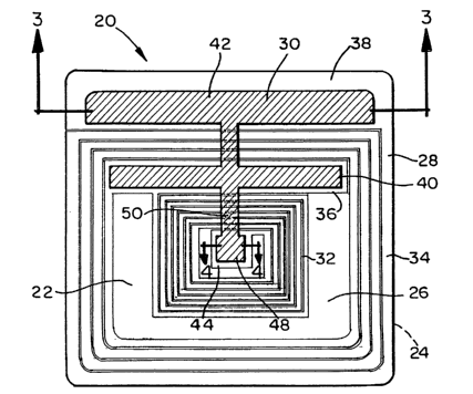
Fig. 2 is a top plan view of a security tag 20 in accordance with a first
implementation or embodiment of the resonant circuit 10 shown in Fig. 1. The
security tag 20 as
8
CA 02402601 2002-09-06
WO 01/71686 PCT/USO1/07093
shown in Figs. 2-4 is comprised of a substantial planar dielectric substrate
22 having a first
principal surface or side 24 and a second, opposite principal surface or side
26. The substrate 22
may be constructed of any solid material or composite structure or other
materials as long as the
substrate is insulative, relatively thin and can be used as a dielectric.
Preferably, the substrate 22 is
formed of an insulated dielectric material, for example, a polymeric material
such as polyethylene.
However, it will be recognized by those spilled in the art that other
dielectric materials may
alternatively be employed in forming the substrate 22. As illustrated in Fig.
2, the substrate 22 is
transparent. However, transparency is not a required characteristic of the
substrate 22.
The circuit components of the resonant circuit 10 as previously described are
formed
on both principal surfaces or sides 24, 26 of the substrate 22 by patterning a
conductive material.
That is, a first conductive pattern 28 (shown in the lighter color of Fig. 2)
is formed on the first side
24 of the substrate 22 which is arbitrarily illustrated in Fig. 2 as the
bottom or backside of the tag
10. A second conductive pattern 30 (shown in the darker color on Fig. 2) is
formed on the second
side 26 of the substrate 22. The conductive patterns 28, 30 may be formed on
the substrate surfaces
24, 26, respectively with electrically conductive materials of a known type
and in a manner which
is well known to those of shill in the electronic article surveillance art.
Preferably, the conductive
material is patterned by a subtractive process (i.e., etching) whereby
unwanted material is removed
by chemical attack after the desired material has been protected, typically
with a printed on etch
resistant ink. In the preferred embodiment, the conductive material is
aluminum. However, other
conductive materials (e.g., gold, nickel, copper, bronzes, brass, high density
graphite, silver-filled
conductive epoxies or the like) can be substituted for the aluminum without
changing the nature of
the resonant cixcuit 10 or its operation. Similarly, other methods (dye.
cutting or the like) may be
employed for forming the conductive patterns 28, 30 on the substrate 22. The
tag 10 may be '
manufactured by a process of the type described in U.S. Patent No. 3,913,219,
entitled "Planar
Circuit Fabrication Process" which is incorporated herein by reference.
However, other
manufacturing processes can be used if desired.
As previously stated, the first and second conductive patterns 28, 30 together
form
the resonant circuit 10 as discussed above. In the embodiment as shown in Fig.
2, both of the
inductances or inductive elements Lp and Ls are provided in the form of
conductive coils 32, 34
respectively, both of which are a part of the first conductive pattern 28.
Accordingly, both of the
9
CA 02402601 2002-09-06
WO 01/71686 PCT/USO1/07093
inductances Lp and Ls are located on the first side 24 of the substrate 22.
Preferably, the two
conductive coils 32, 34 are wound in opposite directions, as shown, to cancel
or at least minimize
inductive coupling. In addition, the first plates 36, 38 of each of the
capacitive elements or
capacitances Cp and Cs are formed as part of the first conductive pattern 28
on the first side 24 of
the substrate 22. Finally, the second plates 40, 42 of each of the
capacitances Cp and Cs are
foamed as part of the second conductive pattern 30 and are located on the
second side 26 of the
substrate 22.
As discussed briefly above, in the security tag 20 a direct electrical
connection
extends through the substrate 22 to electrically connect the first conductive
pattern 28 to the second
conductive pattern 30 to thereby continuously maintain both sides of the
substrate 22 at
substantially the same static charge level. Refernng to Figs. 2 and 4, the
first conductive pattern 28
includes a generally square land.44 on the inner most end of the coil portion
32, Which forms the
first inductance Lp. Likewise,, a generally square land 48 is formed as part
of the second
conductive pattern 30 and is connected by a conductive beam 50 to the portion
of the second
conductive pattern 30, which forms the second plate 40 of the first
capacitance Cp. As shown in
Figs. 2 and 4, the conductive lands 44, 48 are aligned with each other. The
direct electrical
connection is made by a weld through connection 52, which extends between
conductive land 44 of
the first conductive pattern 28 and conductive land 48 of the second
conductive pattern 30 as best
shown in Fig. 4. Preferably, the direct electrical connection 52 between the
lands 44, 48 is formed
by a weld in a manner which is well known to those of ordinary skill in the
EAS art. Referring to
the schematic of Fig. 1, the weld or direct electrical connection 52 is
schematically positioned at
the location.of reference letter A. Because the weld or direct electrical
connection 52 provides a
permanent positive, low resistance electrical connection between the first and
second sides 24, 26 .
of the substrate 22, as well as between the first and second conductive
patterns 28, 30, any static
charge which is present is maintained at the same static charge level on both
sides of the substrate
22. Thus, any potential abrupt change in the static charge level of one side
of the substrate 22, for
example, by touching one side of the substrate 22 to ground, immediately
results in the same static
charge level on the other side of the substrate 22. In this manner, a dramatic
difference in the
voltage potential between the two side of the substrate 22 is avoided to
thereby avoid premature
CA 02402601 2002-09-06
WO 01/71686 PCT/USO1/07093
short circuiting of either of the capacitances Cp, Cs to thereby avoid short
circuiting of either of the
inductances Lp, Ls.
A second implementation or embodiment of a security tag 120 in accordance with
the resonant circuit 10 is illustrated in Figs. 5 and 6. As with the first
embodiment, the security tag
120 is comprised of a substantially planar dielectric substrate 122 having.a
first principal surface or
side 124 and a second opposite principal surface or side 126. Preferably, the
substrate 122 is .
formed of the same material as described above in connection with the first
embodiment.
As with the first embodiment, the circuit components of the resonant circuit
10 are
formed on both principal surfaces 124, 126 of the substrate 122 by patterning
a conductive material
in the same manner as described above in connection with the first embodiment.
Thus, a first
conductive pattern 128 is formed on the first side 124 of the substrate as
illustrated in Fig. 5 and a
second conductive pattern 130 is formed on the second side of the 126 of the
substrate 122 as
illustrated in Fig. 6. This first and second conductive patterns 128, 130
together form the resonant
circuit 10 a discussed above. In the present embodiment, the first inductance
or inductive element
Lp is provided in.the form of a conductive coil 132 which is part of the first
conductive pattern 128
and thus, is located on the first side 124 of the substrate 122. The second
inductance or inductive
elerxient Ls is provided in the form of a conductive coil 134 which is part of
the second conductive
pattern 130 located on the second side 126 of the substrate 122. Preferably,
the two conductive
coils 132, 134 are wound in opposite directions to cancel or at least minimize
inductive coupling.
As with the first embodiment, the first plates 136, 138 of the capacitive
elements or the
capacitances Cp and Cs are formed as part of the first conductive pattern 128
on the first side 124
of the substrate 122. Finally, the second plates 140, 142 of each of the
capacitances Cp and Cs are
formed as part of the second conductive pattern 130 on the.second side 126 of
the substrate 122.
The first conductive pattern 128 further includes a generally square land 144
on the
innermost end of the coil portion 132 which forms the first inductance Lp.
Liltewise, a generally
square land 148 is formed as part of the second conductive pattern 130 and is
connected by a
conductive beam 150 to the second plate 140 of the first capacitance Cp. As
with the first
embodiment, a direct electrical connection is made by a weld through
connection, which extends
between conductive land 144 of the first conductive pattern 128 and conductive
land 148 of the
11
CA 02402601 2002-09-06
WO 01/71686 PCT/USO1/07093
second conductive pattern 130. Referring to the schematic of Fig. l, the weld
or the direct
electrical connection is schematically positioned at the location of reference
letter B. The security
tag 120 as shown in Figs. 5 and 6 functions in the same manner as described
above in connection
with the security tag 20 of Figs. 2-4.
Figs. 8 and 9 illustrate a third implementation or embodiment of a security
tag 220
in accordance with the present invention. The security tag 220 of Figs. 8 and
9 is similar to the
security tag 120 of Figs. 5 and 6. However, in the security tag 220 of Figs. 8
and 9, the inductances
or inductive elements Lp and Ls are split so that each such inductance is
located on each side of the
substrate as will hereinafter be described. A schematic representation of the
security tag 220 is
illustrated in Fig. 7. As shown in Fig. 7, the first inductance is split into
two separate inductances
schematically illustrated as Lp 1 and Lp2. Likewise, the second inductance is
split into two
separate inductances Lsl and Ls2. Inductances Lpl and Lp2 are mutually coupled
as are
inductances Lsl and Ls2.
As with the above-described embodiments, the security tag 220 as shown in
Figs. 8
and 9 is comprised of a substantially planar dielectric substrate 222 having a
first principal surface
224 and a second principal surface 226. 'The substrate 222 is, preferably
formed in a manner as
described above. As with the above-described embodiments, the circuit
components of the
resonant circuit schematically illustrated in Fig. 7 are formed on both
principal surfaces 224, 226 of
the substrate 222 by patterning a conductive material in the manner described
above. That is, a first
conductive pattern 228, shown on Fig. 8, is formed on the first side 224 of
the substrate. Likewise,
a second conductive pattern 230 shown in Fig. 9 is formed on the second side
226 of the substrate
222. The first and second conductive patterns 228, 230 together form the
resonant circuit as shown
in Fig. 7 and as discussed detail above. As illustrated in Fig. 8, inductive
element Lp2 is provided
in the form of a first conductive coil 232 and inductance Ls2 is provided in
the form of a second
conductive coil 233, both of which are part of the first conductive pattern
228. Similarly, as shown
in Fig. 9, inductance Lp 1 is formed as a thixd conductive coil 134 and
inductance Ls 1 is formed as
a fourth conductive coil 135, both of which are part of the second conductive
pattern 230.
Preferably, the first and second conductive coils 232, 233 are wound in
opposite.directions and the
third and fourth conductive coils 234, 235 are wound in opposite directions to
cancel or minimize
inductive coupling. In the security tag 220 as illustrated in Figs. 8 and 9,
the capacitances Cp and
12
CA 02402601 2002-09-06
WO 01/71686 PCT/USO1/07093
Cs are actually distributed capacitances which are implemented by the
conductive pattern portions
which form the conductive coils 232, 233, 234 and 235 in a manner well known
to those of
ordinary skill in the art. .
As with the above-described security tags, the security tag 220 of Figs. 8 and
9
include a direct electrical connection, which extends through the substrate
222 to electrically
connect the first conductive pattern 228 to the second conductive pattern 230
to thereby maintain
both sides of the substrate 222 at substantially the same static charge level.
For this purpose, the
first conductive pattern 228 includes a generally rectangular land 244 on the
inner most end of the
first coil portion 232' which forms inductance Lp2. Similarly, the second
conductive pattern 228
includes a generally rectangular land 248 on the inner most end of the coil
portion 234 which form
the inductance Lp 1. The conductive lands 244 and 248 are aligned with each
other and the direct
connection is made by a weld through connection which extends between the
conductive lands 244,
248 in a manner as described above in connection with the first embodiment.
Referring to the
schematic of Fig. 7, the weld or direct electrical connection is schematically
positioned at the
location of reference letter C. The security tag 220 of Figs. 8 and 9
functions in the same manner
as described above in connection with security tag 20.
From the foregoing description, it can be seen that the present invention
comprises
an activatable/deactivatable security tag, which includes electrostatic
protection for preventing
premature activation or deactivation of the security tag. It will be
appreciated by those skilled in
the art that changes may be made to the above-described embodiment of the
invention without
departing from the broad inventive concepts thereof. For example, the same
inventive concepts
could be employed in connection with activatable/deactivatable security tags
having additional
capacitors, additional inductances or both. It is understood, therefore, that
this invention is not
limited to the particular embodiments disclosed, but is intended to cover any
modifications which
are within the scope and spirit of the invention as defined by the appended
claims.
13