Note: Descriptions are shown in the official language in which they were submitted.
CA 02402850 2002-09-16
WO 01/71824 PCT/EP00/06909
1
METHOD AND DEVICE FOR TRANSFERRING SPIN-POLARIZED
CHARGE CARRIERS
Technical Field
The present invention belongs to the field of organic electronics and
s magnetoelectronics and relates to a method and a device for injecting and
transferring spin-polarized charge carriers, particularly in organic
semiconductors.
Background Art
Control of the spin polarization (SP) of charge carriers injected into
io metallic, semiconducting or insulating materials allows to introduce and
control a new degree of freedom in different electronic devices. A new type
of electronics, known as magnetoelectronics, has been developed on this
basis and has a decisive role in the technology of computers, multimedia
and communications.
is Many types of processors and memory elements for computers are in fact
based on the property of the devices to change their electric resistance
according to the orientation of the spins of the charge carriers, thus
allowing
to read the magnetic information by means of a simple measurement of
resistance (1).
ao The discoveries of materials which exhibit giant magnetoresistance
(magnetic metallic multilayers, GMR) (2) and colossal magnetoresistance
(perovskitic manganites, CMR) (3) lead to an essential improvement in this
field due to the strong electrical signal that can be obtained in these
materials even in low magnetic fields.
Zs GMR materials, discovered in 1988, were used in the computer industry
already in 1994.
Several electronic devices based on CMR materials have been proposed
during the 1990s. These devices comprise both memory elements and
various types of active elements, such as magnetic processors, magnetic
3o transistors and hybrid transistors with inserted superconducting materials.
CA 02402850 2002-09-16
WO 01/71824 PCT/EP00/06909
2
On the one hand, organic electronics has undergone a great development
starting from the 1990s. Essentially, this relates to light-emitting diodes
(LED) and FET transistors. At present, there are no devices in which the
organic material would be used with an active element in
s magnetoelectronics. The use of organic materials in electronics has
advantages, the most important being:
1. The possibility to deposit organic films with low-cost methods even on
a very large deposition area. Differently from semiconducting films, which
require ultrahigh-vacuum techniques, deposition of organic materials can
io occur even in ambient atmosphere.
2. The low cost of said organic materials.
3. The possibility to create flexible devices, for example various color ,
displays.
4. The possibility to vary the colors in optical devices, so as to cover the
is entire visible spectrum.
5. The possibility to reversibly deposit organic films, which can be
subsequently removed and replaced with other materials.
Accordingly, the development and efficiency improvement of organic
electronic devices are of primary importance.
2o In order to produce rnagnetoelectronic devices it is necessary to have the
possibility to create inside the active element of the device spin-polarized
charge carriers. There exist various ways for spin-polarized charge carriers
creation. For example, by illuminating the properly doped GaAs or a similar
semiconductor with circularly-polarized light one excites triplet excitons
as with their spins aligned along the external magnetic field (4]. It is also
known the use spin filters, i.e., devices across which can pass only charge
carriers having a certain spin polarization ~5]. However, such methods are
complicated, expensive, and require the presence of magnetic field.
A third known method is the use of a magnetic material with intrinsic
3o spin polarization. A large fraction of magnetic materials has a larger
number
CA 02402850 2002-09-16
WO 01/71824 PCT/EP00/06909
3
of electrons whose spins are orientated parallel to the magnetic axis (N T ).
Usually, the difference between the larger number of electrons whose spin
orientation is parallel to the magnetic axis and the smaller number of
electrons whose spin is orientated otherwise (N,~) is rather low. For
s example, in Ni this difference is 15-20%. However, there are some
materials, termed half-metallic ferromagnets, whose electron spins are 100%
polarized. These materials include chromium oxide, iron oxide and
manganites of the type Al_XBXMn03 (where A is a rare earth, i.e., La, Nd, et
cetera, and B is a divalent metal, i.e., Ca, Sr, Pb, et cetera).
io The magnetic order of manganites can be described as follows: the
manganese atoms, which can have both 3+ and 4+ valence, have spins S=2
and S=3/2, respectively. Below the Curie temperature (which varies
between approximately 300 and 400 K in these materials), these magnetic
moments arrange themselves in a parallel configuration due to the electron
is exchanges between Mn(3+) and Mn(4+). Due to a strong Hund energy, the
manganese sites accept only electrons whose spins are orientated like their
own magnetic moment. Accordingly, delocalization affects only one half of
all the electrons, i.e., those having spin parallel to the magnetization axis
of
the Mn ions; those with an antiparallel spin remain localized. As a result,
20 100% polarization of the spins of charge carriers (the delocalized
electrons)
is produced.
When two ferromagnetic electrodes with polarized spins come into direct
or tunnelling electric contact, the total electric resistance depends on the
angle of misorientation of their spins: for parallel spins, resistance is
lowest;
zs for antiparallel spins, resistance is highest. This is described in
qualitative
terms by the deGennes formula for the electron transfer probability T12 (6]:
T12 = bl2cos(012/2) + const, (1)
where 1 and 2 correspond to the two ferromagnetic electrodes, b12 is a
tunnelling constant, and 012 is the angle between the magnetic axes of 1 and
30 2. If the external magnetic field is zero, the angle 012 can have any value
CA 02402850 2002-09-16
WO 0~;?~824 PCT/EP00/06909
4
between 0 and 180°. By introducing the magnetic field, both
ferromagnetic
electrodes assume the same oriention, the angle 012 = 0, and the value of T12
reaches its maximum (lowest resistance). This is the cause of negative
magnetoresistance. Owing to very high negative magnetoresistance values
s (up to six orders of magnitude), manganites are known as Colossal
Magnetoresistance (CMR) materials.
In recent times, the fact has been clarified that the value of
magnetoresistance in CMRs is truly high (up to 6 orders of magnitude) only
for electric devices of the tunnelling or point-contact type. Individual
io crystals instead exhibit a magnetoresistance of 2-3% ~7~. Accordingly, the
only magnetoresistance devices that have an application value are tunnelling
or point-contact ones.
Disclosure of the Invention
The aim of the present invention is to provide a method and a device for
is injecting and transporting spin-polarized charge carriers by using, as
medium for charge carrier transport, a low-cost material which can be
deposited with low-cost methods which can be performed easily and in a
reversible manner so that it can be easily replaced with another material if
necessary.
zo An object of the present invention is to provide new active elements for
magnetoelectronics, thereby the resistance of the devices based on such
elements is sensitive to the spin polarization of the carriers passing across
said elements.
Another object is to provide light-emitting diodes (LEDs) with improved
zs efficiency.
Conventional LED light-emitting diodes consist of two electrodes
(electron injectors and hole injectors) between which a layer of
electroluminescent material is placed. During the flow of current between
the two electrodes, excitons, i.e., highly bound electron-hole pairs, are
3o injected into electroluminescent material. The ringlet states generate a
CA 02402850 2002-09-16
w0 W /?182a PCT/EP00/0~9Q9
s
radioactive emission, usually in the visible spectrum, while the triplet
states
generate an emission, which causes delayed phosphorescence [8).
Accordingly, the optical emission of LEDs is generally based on transitions
between singlet states.
s In the two electrodes used in conventional LEDs, all spin polarizations
are present (SP=0), and the statistics of electron spins inside the layer of
organic semiconductor regulates the filling of the exciton states as follows
[9):
1. Singlet (S=0) -> a T p ,~ -> 25 %
io 2. Triplet (S=1) -> a T p T -> 25%
(S=0) -> a T p ,~ + a ,~ p T -> 25 %
(S=-1) -> e,~P,~ -> 25%
Accordingly, spin statistics sets a filling limit of 25% for the S=0 levels,
contributing, together with several other processes, to a reduction in the
is efficiency of LEDs. If one electrode is a half-metallic ferromagnet, all
the
charges injected by said electrode have the same spin, for example -a T . If
one observes the above spin statistics, it is evident that only the
combinations that do not have electrons with a ,~ electron spin are now
possible. Accordingly, the levels a T p,~ and a T p T are filled, and this
changes
2o from 25% to 50% the filling of the singlet layers. The additional use of a
second spin-polarized electrode as holes injector leads to a 100% S=0 level
filling, with a 75% improvement in the efficiency of the LED.
The statistical considerations presented above are based on the
arguments discussed in classical manuals of quantum mechanics and
2s therefore experimental tests are not necessary. On the other hand, to
realize
such a selective filling of a chosen exciton level (singlet in our case) it is
important the charge carriers to not lose their spin orientation after
escaping
out of the electrode. What the inventors of the present invention have found
is that the electrons (holes), once injected into the organic material, do not
30 lose memory of the spin orientation that they had in the electrode.
CA 02402850 2002-09-16
WO 01/71824 PCT/EP00/06909
6
Accordingly, another object of the present invention is to provide a
method and a device which allow an increased filling of the singlet exciton
states, which are optically active in the electroluminescent material.
The above-mentioned objects and others which will become apparent
s from the present description are achieved with a method according to the
invention for transferring chaxge carriers, comprising the steps of:
a) injection of spin-polarized charge carriers in an organic material and
b) transport of said spin-polarized charge carriers through said organic
material.
to The organic material is an organic material capable of carrying an
electric current, preferably an organic material chosen from the group
constituted by polythiophenes and metal-phthalocyanines.
A preferred example is constituted by the organic materials
sexithiophene and zinc-phthalocyanine.
is The organic material can be in the form of a thin layer having a thickness
suitable to ensure the electrical continuity of the material.
The injection of step a) is preferably performed by means of the flow of
electric current between two electrodes through a layer of organic material.
The two electrodes are made of materials having substantially 100% spin
ao polarization of the charge carriers and are termed spin-polarized
electrodes.
Preferably, the two electrodes are constituted by ferromagnetic
manganites having the formula Al_XBXMn03.
A preferred example is constituted by electrodes made of Lao.~Sro.3Mn03.
The transfer of charge carriers of step b) can be performed by applying
Zs an electric field to said organic material, particularly an electric field
E >_ 104
- 105 V/cm.
Description of preferred embodiments
An embodiment of the present invention relates to a method for inducing
magnetoresistance in an organic material, which comprises the steps of:
3o a) injection of spin-polarized charge carriers in an organic material from
CA 02402850 2002-09-16
w0 01!7184 PCT/EP00!06909
a spin-polarized electrode,
b) transport of said spin-polarized charge carriers through said organic
material, between said spin-polarized electrode and a second spin-polarized
electrode with application of an external magnetic field.
s Another aspect of the present invention relates to a device for
transferring charge carriers, comprising:
a) means for injecting spin-polarized charge carriers, and
b) a medium suitable for the transport of spin-polarized charge carriers,
said medium suitable for the transport of spin-polarized charge carriers
io comprising an organic material.
The organic material is an organic material capable of carrying electric
current.
Preferably, the organic material is chosen from the group constituted by
polythiophenes and metal-phthalocyanines. A preferred example is
is constituted by sexithiophene and zinc-phthalocyanine.
The organic material can be in the form of a thin layer, with a thickness
suitable to ensure the electrical continuity of the material.
The means for injecting the spin-polarized charge carriers are preferably
made of a material with 100% spin polarization of the charge carriers, more
zo preferably ferromagnetic manganites having the formula Al_XBXMn03. The
injection means are even more preferably made of Lao.~Sro.3Mn03.
In one embodiment, the device according to the invention furthermore
comprises means for applying an electric field to said material suitable to
transport charge carriers.
2s In another embodiment, the device according to the present invention
comprises an organic material which is an electroluminescent material,
means for injecting spin-polarized charge carriers which are constituted by a
first spin-polarized electrode and a second spin-polarized electrode, the
first
electrode being an electrode for injecting spin-polarized electrons and the
3o second electrode being an electrode for injecting spin-polarized holes, the
CA 02402850 2002-09-16
WO 01/71824 PCT/EP00/06909
8
device being suitable for use as light-emitting diode.
In another embodiment, the invention relates to a device for inducing
magnetoresistance in an organic material, comprising:
a) means for injecting spin-polarized charge carriers, comprising a first
s spin-polarized electrode and a second spin-polarized electrode, and
b) a medium suitable for the transport of spin-polarized charge carriers,
the medium for the transport of spin-polarized charge carriers comprising
the organic material interposed between said first and second spin-polarized
electrodes, and
io c) means for applying an external magnetic field.
Preferably, the devices according to the present invention comprise
means for injecting spin-polarized charge carriers constituted by two
electrodes which are in mutual tunnelling contact through the organic
material, the magnetic polarization of the first and second electrodes can be
is changed separately by applying local magnetic fields, preferably stronger
than 3000 Oe, and the device is suitable for use as memory element.
Furthermore, the device according to the present invention can comprise a
cathode which emits spin-polarized electrons, said cathode being made of
materials having substantially 100% spin polarization of the charge carriers,
2o and being covered by a protective layer formed by said organic material.
The inventors of the present invention have found that the charge
carriers, once injected into an organic material, do not lose memory of the
spin state that they had in the electrode. This fact leads to a change in the
exciton state filling statistics. In the case of injection of charges having
the
2s same spin (i.e., spin-polarized charges), for example a T, as regards the
above cited spin statistics, only the combinations in which there are no
electrons with e,~ electron spin remain possible. In this case, only the
levels
a T p ~, and a T p T are filled; therefore, statistically, the filling of the
singlet
states changes from 25% to 50%. Likewise, by using an injection of holes
3o which also are spin-polarized (with the same spin), the S=0 singlet state
CA 02402850 2002-09-16
WO 01/71824 PCT/EP00/06909
9
filling statistics changes to 100%, i.e., yielding a 75% increase in the
efficiency of the light-emitting device.
In order to examine the possibility to perform spin-polarized injection in
a layer of organic material and to perform spin-polarized coherent transport
s through said organic material, the inventors of the present invention used
devices, according to the invention, based on spin-polarized materials and
vanous organic materials.
Lao.~Sro_3Mn03, which is a typical representative of the Al_XBXMn03
system, was used as spin-polarized material.
io Thin films of Lao.~Sro.3Mn03 were deposited with the Channel-Spark
ablation method on substrates of neodymium gallate or strontium titanate.
The thickness of the film used varies between 50 and 200 nm, allowing to
provide in the film a highly ordered crystallographic structure and electrical
and magnetic properties similar to those of single crystals.
is The micro-Raman spectrum of a film on neodymium gallate is shown in
Figure 1, which shows the micro-Raman spectra of a typical ferromagnetic
film, of the single crystal of Lao.~Sro.3Mn03, and of the neodymium gallate
substrate.
It is noted that the quality of the film is very high, showing the complete
zo absence of spurious phases (only the peaks of the substrate and those of
the
Lao_~Sro.3Mn03 are present).
The magnetic measurements show a Curie temperature which abundantly
exceeds the ambient temperature, i.e., T~ = 375K, as shown by Figure 2
(which plots magnetic moment over temperature for a typical ferromagnetic
2s film and for the single crystal of Lao.~Sro.3Mn03). This allows to work
with
the films in the ferromagnetic state at ambient temperature.
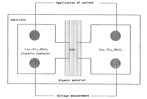
After the deposition of the Lao.~Sro.3Mn03 films, nanoscopic devices were
created as shown in Figure 3, which illustrates two spin-polarized electrodes
separated by a nanogap prepared by applying a nanoscopic technique.
3o The gaps vary between 70 and S00 nm for the various films used.
CA 02402850 2002-09-16
WO 01/71824 PCT/EP00/06909
The measurements of resistance across the gap yielded infinite
resistance. Accordingly, the CMR electrodes are completely separated.
The consecutive step for producing the device was the provision of an
organic bridge between the two electrodes.
s Organic films were deposited by means of the thermal vaporization
method through the masks in order to create a stripe, which covers the gap
and leaves the two electrodes open (Figure 3).
The organic materials used are sexithiophene and zinc-phthalocyanine.
Since both are nonmagnetic materials, in normal conditions they can have
to no negative magnetoresistance, i.e., a decrease in resistance due to the
alignment of the localized magnetic moments. Repeated measurements
conducted by us both on the sexithiophene films and on the zinc-
phthalocyanine films have confirmed the total absence of negative
magnetoresistance when nonmagnetic electrodes (gold, silver paste) are
is used. In organic materials of this type, a weak positive magnetoresistance
can be measured X10), but only in very intense magnetic fields (over 60-80
kOe).
Tunnelling-type experiments were conducted in order to examine the
possibility of injecting spin-polarized charge carriers from the spin
Zo polarized ferromagnetic electrodes.
The transfer of the spins through the material was examined by inserting
the organic material between the two spin-polarized electrodes. One of the
ferromagnetic electrodes emitted spin-polarized charges, and the other one
acted as detector, sensitive to the angle O of the incoming spins. In order to
2s reveal the presence or absence of an interference of the organic material
with the orientation of the electron spins, the influence of the variation of
the magnetic field on the resistance of the device was studied. Negative
magnetoresistance of the ferromagnet-organic material-ferromagnet device
would demonstrate that the organic material does not change, or only
3o partially changes, the orientation of the spins of the charge carriers that
pass
CA 02402850 2002-09-16
WO 01/71824 PCT/EP00/06909
11
through it. Negative magnetoresistance is caused by the alignment of the
spins in the two ferromagnetic electrodes under the action of the magnetic
field. If instead the resistance of said device would show no dependency on
the magnetic field except for the possible intrinsic magnetoresistance of the
s organic material (which is zero in the case of the experiments conducted),
the conclusion is that the spins lose their initial orientation inside the
organic material or at the ferromagnet-organic interface.
Figure 4 shows the magnetoresistance measured on a tunnelling device
of the (ferromagnet)-(organic material)-(ferromagnet) type, particularly of
to the Lao..,Sro.3Mn03 - sexithiophene - Lao.~Sro.3Mn03 type. The thickness of
the ferromagnetic material is 100 nm, the gap between the electrodes is 100
nm and the thickness of the organic film is 125 nm. The resistance of the
device across the organic layer was measured by using a picoammeter at
various voltages. The measurements were conducted at ambient temperature
is and in a normal atmosphere (without vacuum).
Resistance changes from approximately 3.35 GSZ with zero magnetic
field (black curve) to 2.95 GSZ with the insertion of 3.4 kOe at right angles
to the surface (curve 2), yielding a magnetoresistance of ~15%. Immediately
after shutting down the magnetic field (t < 1 min), the resistance reaches an
Zo intermediate state (curve 3), which is due to a residual alignment of the
electrodes which is higher than the initial one. After 10-15 minutes, the
resistance returns to the initial values (curve 1). The measurements were
repeated several times. After ending a set of measurements, the organic
material was dissolved and deposited again. By repeating this procedure
zs four times, it was found that the results were reproducible for each
nanogap.
The maximum value of 15% (approximately 5%/kOe) for magnetoresistance
observed in devices with sexithiophene is comparable with the values that
occur in commercial devices used in magnetoelectronics (1]. This value
could be increased further if magnetoresistance were measured as difference
3o between antiparallel alignment and parallel alignment. The
CA 02402850 2002-09-16
I~VO 01/71824 PCT/EP00/0690Q
12
magnetoresistance value decreases with the width of the cap and is 10% for
200-nm gaps and 0% for 300-nm gaps. This last fact confirms once again
the absence of intrinsic negative magnetoresistance in sexithiophene, since
it is a direct measurement on the device being considered. The coherence
s length is therefore estimated at 200-300 nm at ambient temperature.
The change of the polarization of the spins during transfer through a
certain material can occur essentially for two reasons: due to scattering on
the magnetic centers or due to spin-orbital interaction. Sexithiophene
contains no magnetic atoms and the spin-orbital interaction in this type of
io material is very low due to the absence of heavy atoms. The polarized
(coherent) transfer of the spins observed with the experiments thus becomes
possible.
The same experiment was repeated by using as organic material zinc-
phthalocyanine, which is very different from sexithiophene owing to the
is presence of a metallic atom in the molecule.
The presence of the metallic atom must increase the effect of the spin-
orbital interaction, causing a reduction, if not the elimination, of spin-
polarized transfer. Figure 5 shows the measurements of resistance with and
without magnetic field of a device similar to the one shown in Figure 4. The
20 organic material is a film of zinc-phthalocyanine 100 nm thick; the
ferromagnetic material is the same material (Lao.~Sro.3Mn03), and the gap
that separates the electrodes is approximately 80 nm. The resistance was
normalized with respect to the resistance of the device in the absence of the
magnetic field. The magnetic fields applied were both parallel to the
2s substrate (+) and antiparallel thereto (-), and 1 % magnetoresistance was
observed. This experiment, too, was repeated several times, and high
reproducibility of the results was observed. Accordingly, spin-polarized
transfer was confirmed for zinc-phthalocyanine also.
Generalizing the results obtained on two organic materials having very
3o different electrical properties, one can conclude that the possibility of
spin-
CA 02402850 2002-09-16
WO 01_%?18~4 PCT/EP00/06909
13
polarized injection and the transfer of charges with substantially polarized
spins through thin organic layers (up to 200-300 nm) without magnetic
moment has been demonstrated for the first time. It is very important to
stress that these effects were observed at ambient temperature and in a
s normal atmosphere, thus paving the way for several applications. The
electric fields used to transport the charge carriers across the tunnels were
104-10' V/cm for both organic materials.
In any case, it is important to note that the organic materials used, despite
being very different from each other, have no intrinsic magnetic moment
to and therefore are weak paramagnets. At present, the effect of any magnetic
moment of the organic layer on the spin-polarized transfer is not known. On
the other hand, at ambient temperature, almost all the organic materials are
paramagnetic; ferromagnetism in organic materials usually occurs at very
low temperatures (<50 K). Accordingly, in normal conditions the spin-
es polarized transfer effect must be common for most organic conductors. It
should be noted that organic materials (evidently) oppose a certain
"magnetic resistance" to spin-polarized transfer, like any ordinary electrical
conductor opposes a resistance R to the transfer of electric charges. This is
also evident from the difference between sexithiophene and zinc-
ao phthalocyanine. Accordingly, it has been demonstrated that organic
materials can be conductors of the polarization of the spins of charge
carriers, but there is no evidence that they can be spin polarization
superconductors.
The present invention, based on the possibility to substantially control
2s spin polarization (SP) of the charge carriers injected in semiconductor
devices (inorganic and organic ones) allows to control a hitherto
uncontrolled parameter which has a primary importance in electrooptical
and electromagnetic processes.
Furthermore, the present invention allows creating new kinds of devices,
3o combining CMR materials with organic materials and inserting as active
CA 02402850 2002-09-16
WO 01/71824 PCT/EP00/06909
14
material a material which is optically highly nonlinear and thus providing a
further boost to magnetoelectronics.
Furthermore, the present invention provides a process for injecting
polarized spins in organic semiconductors and for spin-polarized transfer
s across organic semiconductors.
The experiments conducted used devices which included two spin-
polarized electrodes of material separated by a narrow nanogap and
connected, across said gap, by a bridge of organic material. The spin-
polarized charge carriers were injected from electrodes into the organic
io material and crossed it, maintaining their polarization. The useful signal
consisted of the magnetoresistance measured across the device.
The invention illustratively disclosed suitably may be practiced in the
absence of any element and/or step which is not specifically disclosed
herein.
is The disclosure of Italian Patent Application No. MI2000A000603 from
which the present invention claims priority is herein incorporated by
reference.
REFERENCES
1. G.A. Prinz, Science, vol. 282, 1660 (1998)
20 2. M.N. Baibich, J.M. Broto, A. Fert, F. Nguyen Van Dau, F. Petroff, P.
Etienne, G. Greuzet, A. Friederich, J. Chazelas, Phys. Rev. Lett., Vol. 61,
2472 ( 1988)
3. S. Jin, T.H. Tiefel, M. McCormack, R.A. Fastnacht, R. Ramesh, L.H.
Chen, Science, vol. 264, 413 (1994)
~s 4. W. Nabhan, Y. Suzuki, Appl. Phys. A, vol. 66, S101 (1998);
M. Oesterech, J. Hubner, D. Hagele, P.J. Klar, W. Heimbrodt, W.W. Riihle,
D.E. Ashenford, B. Lunn, Appl. Phys. Lett., vol. 74, 1251 (1999)
5. A. Filipe, Materials Research Society Symposium Proceedings, vol.
475, 75 (1997);
~o H. Batelaan, A.S. Green, B.A. Hitt, T.J. Gay, Phys. Rev. Lett., vol. 82,
4216
CA 02402850 2002-09-16
WO 01/71824 PCT/EP00/06909
(1999)
6. P.-G. deGennes, Phys. Rev., v. 118, 141 (1960)
7. H.Y. Hwang, S.-W. Cheong, N.P. Ong, B. Batlogg, Phys. Rev. Lett.,
vol. 77, 2041 (1996)
s 8. J. Kalinowski, NATO ASI SERIES 3 HIGH TECHNOLOGY, 1997,
vol. 24, pages 167-206;
R.H. Friend, R.W. Gymer, A.B. Holmes, J.H. Burroughes, R.N. Marks, C.
Taliani,
D.D.C. Bradley, D.A. Dos Santos, J.L. Bredas, M. Logdlund, and W.R.
to Salaneck, Nature 397, 121 (1999)
9. F. Cacialli, Phil. Trans. R. Soc. Lond. A, vol. 358, 173 (2000);
A.L. Burin, M.A. Ratner, J.Chem.Phys. vol. 109, 6092 (1998)
10. D. Delabouglise, D. Berner, J.-P. Travers, Synthetic Metals, vol. 101,
377 (1999)
is 11. US patent 5874749: Polarized optical emission due to decay or
recombination of spin-polarized injected carriers
12. US patent 4823177: Method and device for magnetizing thin films by
the use of injected spin-polarized current
13. US patent 5872368: Method of controlling a superconductor
Zo 14. US patent 5838020: Method and apparatus for storing data using
spin-polarized electrons
15. US patent 5723978: Photo-inducible magnetic exchange coupling
device.