Note: Descriptions are shown in the official language in which they were submitted.
CA 02403048 2002-09-10
WO 01/93409 PCT/USO1/12907
-1-
Description
LOW POWER VOLTAGE REGULATOR CIRCUIT
FOR USE IN AN INTEGRATED CIRCUIT DEVICE
TECHNTCAL FIELD
The invention relates to voltage regulator
circuits, and more particularly to a circuit that re-
ceives an external power supply voltage as an input and
provide as an output a specified level of voltage for an
internal circuit of an integrated circuit device.
BACKGROUND ART
In the field of integrated circuits, compati-
bility requires the use of a conventional 5V power supply
for most circuit devices. Also, compatibility requires
many TTL circuits to work at a conventional 5V external
power supply voltage. However, when the degree of inte-
gration increases, many circuits are manufactured to work
at a lower voltage (such as 3V) in order to lower power
consumption and reduce excessive electrical field.
Therefore, there is a need for voltage regulator circuits
(voltage stepdown circuits) arranged inside the devices
to convert the high voltage level (5V) of an external
power supply down to a desired level (3V-4V) and to sup-
ply that voltage to the internal circuit of the device.
Many designs of the voltage regulator circuit exist.
Fig. 7 shows a conventional internal stepdown
circuit 17 that is also described in the background art
section of U.S. Patent No. 5,189,316 to Murakami et al.
The illustrated internal stepdown circuit 1'7 essentially
consists of a reference voltage generator circuit 100 and
an internal voltage control circuit 200. The reference
voltage generator circuit 100 is adapted to generate a
reference voltage VREF with respect to the internal volt-
CA 02403048 2002-09-10
WO 01/93409 PCT/USO1/12907
-2-
age control circuit 200, and includes p-channel MOS
(PMOS) transistors 111-115. The PMOS transistors 111-113
are connected in series to each other and are interposed
between a supply input terminal 300 and ground GND.
These PMOS transistors 111-113 are used as resistors,
respectively, and constitute a resistive potential di-
vider circuit. The supply input terminal 300 receives a
supply voltage Ext.VCC from an external power supply (not
shown). Other PMOS transistors 114 and 115 are connected
in series to each other, and are interposed between the
supply input terminal 300 and the ground GND in parallel
to the above described PMOS transistors 111-113.
The internal voltage control circuit 200 is
adapted to correct an internal voltage VINT based on the
reference voltage VREF so as to prevent the fluctuation
of the internal voltage VINT which may be caused by the
fluctuation of the supply voltage Ext.Vcc, and is formed
of a current quantity switching circuit 210, a voltage
comparator circuit 220 and an output transistor P225.
The current quantity switching circuit 210 is adapted to
switch a current quantity supplied to the voltage com-
parator circuit 220 in accordance with switching between
an active mode and a standby mode of the semiconductor
integrated circuit device, and is formed of two PMOS
transistors P211 and P212 interposed in parallel between
the supply input terminal 300 and the voltage comparator
circuit 220. The voltage comparator circuit 220 is
adapted to make a comparison between the reference volt-
age VREF applied from the reference voltage generator
circuit 100 and the internal voltage VINT supplied from
the output transistor P225 and to control a conductivity
of the output transistor P225 in accordance with a result
of the comparison. The voltage comparator circuit 220 is
formed of two PMOS transistors P223 and P224 and two
N-channel MOS (NMOS) transistors N221 and N222.
CA 02403048 2002-09-10
WO 01/93409 PCT/USO1/12907
-3-
The reference voltage generator circuit 100
generates a constant reference voltage, VREF, which is
supplied to the voltage comparator circuit 220. When the
semiconductor integrated circuit device provided with the
internal stepdown circuit 17 shown in Fig. 7 is in an
active mode, the clock signal CS supplied to the current
quantity switching circuit 210 is at a low level (logic
level = 0). Therefore, the PMOS transistor P211 is kept
on in the active mode. Meanwhile, the PMOS transistor
P212 is always in the on state because its gate is con-
nected to the ground GND. Therefore, both the PMOS tran-
sistors P211 and P212 are turned on in the active mode,
and thus a large current is supplied to the voltage com-
parator circuit 220. The voltage comparator circuit 220
compares the reference voltage VREF with the internal
voltage VINT. ln~h.en the voltage VREF becomes smaller than
the voltage VINT, for instance, due to the increase of
the internal voltage VINT caused by the increase of the
supply voltage Ext.Vcc or other reasons, the conductivity
of the PMOS transistor P224 decreases. Correspondingly,
the potential at the drain of the PMOS transistor P224
decreases, and thus the conductivity of the NMOS transis-
tor N221 decreases. Consequently, the potential at the
drain of the NMOS transistor N1 increases, resulting in
reduction of the conductivity of the output transistor
P225. Accordingly, the internal voltage VINT decreases
to the same value as the voltage VREF (VINT = VREF).
Conversely, if the internal voltage VINT decreases to a
value less than the reference voltage VREF (VREF > VINT)
the circuit 17 operates in a manner opposite to that
described above to maintain the internal voltage VINT at
the reference voltage VREF.
As described above, the internal stepdown cir
cuit of Fig. 7 generates the internal voltage VINT inde
pendent of the supply voltage Ext.Vcc. This internal
CA 02403048 2002-09-10
WO 01/93409 PCT/USO1/12907
-4-
voltage VINT is applied to respective internal circuits
in the semiconductor integrated circuit device.
When the semiconductor integrated circuit de-
vice provided with the internal stepdown circuit 17 of
Fig. 7 is in a standby condition, the clock signal CS is
at the "H" level and the PMOS transistor P211 is main-
tained in an off state. Consequently, the current quan-
tity supplied from the current quantity switching circuit
210 to the voltage comparator circuit 220 is reduced,
resulting in reduction of the consumption power in the
standby mode.
As described above, the internal stepdown cir-
cuit of the prior art shown in Fig. 7 is intended to
reduce the consumption power in the standby mode by set-
ting the PMOS transistor P211 at the off state in the
standby mode. However, even when the PMOS transistor
P211 is turned off, a current is supplied to the voltage
comparator circuit 220 in the standby mode through the
PMOS transistor P212, because this PMOS transistor P212
is turned on. Further, the internal stepdown circuit of
the prior art shown in Fig. 7 has structures in which the
current flows in the reference voltage generator circuit
100 even in the standby mode.
Other prior art inventions try to reduce power
consumption of the reference voltage generator circuit
100 and the internal voltage control circuit 200 by plac-
ing transistors as switches in series with these circuits
in order to turn them off during standby mode. However,
this does not significantly reduce the power consumption
of the circuits because during active mode these circuits
still consume power.
Therefore, the internal stepdown circuits of
the prior art, such as the circuit shown in Fig. 7, still
have a serious problem in that the consumption. power
cannot be sufficiently reduced. Many prior art circuits
CA 02403048 2002-09-10
WO 01/93409 PCT/USO1/12907
-5-
burn approximately 1 mA or greater of the supply current.
Moreover, the circuits are rather complicated and many
prior art circuits require the use of a operational am-
plifiers and band gap references, making the circuits
large anal power consuming.
An.object of the present invention is to pro-
vide a circuit that has low power consumption and which
burns approximately 0.5 ~zA of the supply current, which
is much lower than in the prior art.
Another object of the present invention is to
provide a simple voltage regulator circuit that occupies
a small area and does not require the use of an opera-
tional amplifier.
SUMMARY OF THE INVENTION
The above objects have been achieved in the
present invention, which provides a voltage regulator
circuit that can be described as being made up of a volt-
age monitoring subcircuit, a voltage tracking subcircuit
and a plurality of voltage maintaining subcircuits with
an input and an output. The voltage tracking subcircuit
functions to have the output voltage track the input
voltage when the input voltage increases from zero volts.
The voltage maintaining subcircuits function to clamp the
output voltage at the desired voltage for an internal
circuit whether the input voltage remains at that desired
voltage or continues to rise to a higher voltage. The
voltage monitoring subcircuit functions to disable the
voltage tracking subcircuit when the input voltage con-
tinues to rise above the desired voltage for the internal
circuit and to enable the appropriate ones of the voltage
maintaining subcircuits to control the amount of voltage
drop with respect to the input voltage so that the output
voltage stays at the desired voltage for the internal
circuit. The voltage regulator circuit of the present
CA 02403048 2002-09-10
WO 01/93409 PCT/USO1/12907
-6-
invention is mainly comprised of CMOS inverters which
consume very little power.
BRIEF DESCRIPTION OF THE DRAWINGS
Fig. 1 is a schematic block diagram of the
voltage regulator circuit of the present invention.
Fig. 2 is an electrical circuit diagram of a
first embodiment of the voltage regulator circuit of Fig.
1.
Fig. 3 is an electrical circuit diagram of a
second embodiment of the voltage regulator circuit of
Fig. 1.
Fig. 4 is a graph of the external voltage Vcc
(input) vs. the Vcc internal signal (output) of the volt-
age regulator circuit of Fig, 1.
Fig. 5 is a schematic block diagram of the
preferred embodiment of the voltage regulator circuit of
the present invention.
Fig. 6 is an electrical circuit diagram of the
voltage regulator circuit of Fig. 5.
Fig. 7 is a circuit diagram illustrating a
conventional internal stepdown circuit as known in the
prior art.
BEST MODE FOR CARRYING OUT THE INVENTION
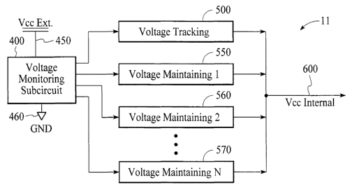
With reference to Fig. 1, the voltage regulator
circuit of the present invention 11 includes a voltage
monitoring circuit 400 which receives an external volt-
age, Vcc external 450, as the input to the circuit and is
also connected to ground 460. The output of the voltage
monitoring circuit 400 is supplied to a voltage tracking
subcircuit 500 and to a plurality of voltage maintaining
subcircuits 550, 560, 570. These subcircuits produce an
output voltage at an output 600 which is a Vcc internal
signal to an internal circuit of a device. As the Vcc
CA 02403048 2002-09-10
WO 01/93409 PCT/USO1/12907
-7_
external voltage 450 increases from zero volts to the
desired voltage level for the output 600, the voltage
tracking subcircuit 500 provides the voltage at output
600 at the same level as VcC external 450. As VcC exter-
nal 450 increases to (1 x ~tTT~) threshold above the de-
sired output voltage, where ~VT~ is the threshold voltage
of the PMOS and NMOS transistors in the voltage regulator
circuit 11, the voltage tracking subcircuit 500 turns off
and the first voltage maintaining subcircuit 550 turns
on, to maintain the output voltage at the desired volt-
age. As the Vcc external increases to (2 x fVT~) above
the desired voltage level, the first voltage maintaining
subcircuit 550 turns off and the second voltage maintain-
ing subcircuit 560 turns on to keep the output at the
desired voltage level. Additional voltage maintaining
subcircuits may be implemented to maintain the output
voltage at the desired level through further increases in
VcC external. The voltage regulator circuit 11 continues
to function as described above until the final voltage
maintaining subcircuit 570 is utilized.
With reference to Fig. 2, a first embodiment 12
of the present invention is shown. The voltage monitor-
ing circuit 401 is comprised of a chain of diodes Con-
nected in series. Each of these diodes can be imple-
mented by an NMOS transistor having its gate connected to
its drain, These diodes operate as a voltage divider.
Each diode in the voltage monitoring circuit 401 repre-
sents a voltage drop of one threshold voltage, or (1 x
fVT~). The first diode 431 in the chain of diodes has an
input connected to the VCC external voltage 450. The
voltage tracking subcircuit 501 connects to the voltage
monitoring circuit 401 at node 410, while the first volt-
age maintaining subCircuit 551 and the second voltage
maintaining subcircuit 561 connect to the voltage moni-
toying subcircuit 401 at node 411. Subsequent voltage
CA 02403048 2002-09-10
WO 01/93409 PCT/USO1/12907
-g_
maintaining subcircuits connect at nodes further down the
chain of diodes, such as at node 412 and node 413. The
last diode 437 of the chain of diodes is connected to the
ground potential 460.
The voltage tracking subcircuit 501 consists of
a PMOS transistor P501 having a gate connected to a node
410 in the voltage monitoring circuit 401, a source con-
nected to Vcc external, and a drain connected to the
output 601. The first voltage maintaining circuit 551
consists of a PMOS transistor P551 having a gate con-
nected to a second node 411 in the voltage monitoring
circuit 401, a source connected to Vcc external, and a
drain connected to the gate of an NMOS transistor N551.
Transistor N551 has a drain connected to Vcc external and
a source connected to the output 601. The second voltage
maintaining circuit 561 consists of a multiplexes 701
having a high input 711 connected to the second node 411
of the voltage monitoring circuit 401, a low input con-
nected to the ground potential, a clock input 712, and an
output 714 connected to the gate of an NMOS transistor
N561. The NMOS transistor N561 has a drain connected to
Vcc external and a source connected to the output 601.
The third voltage maintaining circuit 571 consists of a
multiplexes 702 having a high input 721 connected to a
third node 412 of the voltage monitoring circuit 401, a
low input 720 connected to the ground potential, a clock
input 722 and an output 724. The output 724 of the
multiplexes 702 is connected to an inverter 713 which
provides an inverted clock signal at the clock input 712
of the multiplexes 701 of the prior voltage maintaining
circuit 561. The output 724 of multiplexes 702 is also
connected to the gate of an NMOS transistor N571, which
has a drain connected to Vcc external and a source con-
nected to the gate of a second NMOS transistor N573.
Transistor N573 has a drain connected to Vcc external and
CA 02403048 2002-09-10
WO 01/93409 PCT/USO1/12907
_g_
a source connected to the gate of a third NMOS transistor
N575. Transistor N575 has a drain connected to Vcc ex-
ternal and a source connected to the output 601. Subse-
quent voltage maintaining subcircuits may be added to the
voltage regulator circuit. Each subsequent voltage main-
taining circuit would be constructed in a similar manner
to the third voltage maintaining subcircuit 571, except
that an additional NMOS transistor would be added for
each subsequent voltage maintaining subcircuit (i.e. the
second subcircuit 561 has two NMOS transistors, the third
subcircuit 571 has three NMOS transistors, a fourth
subcircuit would have four NMOS transistors, etc.,.).
For the purposes of explanation, assume that
the output voltage at output 601 is desired to be main-
tamed at 3 volts. Also, assume that the voltage thresh-
old drop ~TT~ across each diode is 1 volt. Tn~hen Vcc
external 450 starts to increase from zero volts, the node
410 in the diode chain is at a low logic level. This low
logic level turns on the PMOS transistor P501 in active
mode, allowing the Vcc external applied to the source of
PMOS transistor P501 to pass through to the output 601 of
the circuit. When Vcc external 450 increases to the
desired voltage level, in this case 3 volts, there is a
(3 x fVT~) voltage drop, corresponding to a (1 x ~VT~)
voltage drop across each of the diodes 431, 432, and 433,
such that the node 410 remains at a low logic level. As
the input voltage, Vcc external, increases beyond the
desired voltage level, node 410 transitions to a high
logic level, which turns off PMOS transistor P501 which
shuts off the voltage tracking subcircuit 501.
Initially, node 411 is also at a low logic
level and this turns on PMOS transistor P551 of the first
voltage monitoring circuit 551. However, when the output
voltage is less than the desired voltage level, NMOS
transistor N551 is off because the voltage level at the
CA 02403048 2002-09-10
WO 01/93409 PCT/USO1/12907
-10-
gate of transistor N551, Vcc external through transistor
P551, is equal to the voltage level at the source of
N551, since Vcc external is equal to Vcc internal.
Therefore, there is no voltage threshold ~VT~ difference
across transistor N551, which would be necessary in order
to turn on transistor N551. After the voltage tracking
subcircuit 501 is turned off, the voltage at the source
of transistor N551 starts to fall as the output voltage
Vcc internal at output 601 starts to decrease. When the
voltage Vcc internal at output 601, and therefore the
voltage at the source of transistor N551, reaches (1 x
f(TT~) below the gate voltage of transistor N551, transis-
tor N551 turns on. Thus, the first voltage maintaining
subcircuit 551 is turned on and passes a voltage of (Vcc
external - 1 ~TT~) to the output 601 to maintain the
output voltage at the desired voltage level until the
external Vcc increases by another (1 x fVT~) volts. After
the external voltage increases by (1 x ~TT~) the node 411
transitions to a high logic level which turns off tran-
sistor P551 and thus shuts down the first voltage main-
taining subcircuit 551.
Initially, when node 411 is at a low logic
level, the second voltage maintaining subcircuit 561 is
off. The low signal is passed first to a multiplexer 701
and since at this point the clock input 712 is at a high
logic level, the high input 711 to the multiplexer pro-
ceeds to the output 714, which passes the low signal to
the gate of transistor N561. This turns transistor N561
off. When the node 411 transitions to a high signal, the
high signal passes through the multiplexer 701 to pass
the high signal to NMOS transistor N561, turning N561 on.
This turns on transistor N563 which passes the Vcc exter-
nal signal, a voltage of (Vcc external - 2 ~VT~) to the
output 601. Since, at this point, the external voltage
is (2 x EVT~) above the desired output level, the (1 x
CA 02403048 2002-09-10
WO 01/93409 PCT/USO1/12907
-11-
~TT~) voltage drops across each of transistors N561 and
N563 maintain the output voltage at the desired level.
After the Vcc external reaches a voltage higher
than (Vcc external + 2 ~VT~), node 412 transitions from
low to high. Initially, node 412 is low and the low
signal proceeds through multiplexer 702 to provide a low
signal at the multiplexer output 714. This causes tran-
sistor N571 to be turned off, which results in the next
voltage maintaining subcircuit 571 being off. The low
signal at 714 goes to an inverting amplifier to provide a
high signal at the clock input 712 of multiplexer 701
which lets the high signal at input 711 pass through the
multiplexer to the gate of transistor N561 to turn on the
second voltage maintaining subcircuit 561 as described
above. When node 412 becomes high, the high signal pro-
ceeds through multiplexer 702 and is supplied to invert-
ing amplifier 713 which provides a low signal to the
clock input 712 of multiplexer 701, which turns off
multiplexer 701 and shuts down the subcircuit 561. The
high signal also passes through multiplexer 702 to turn
on the next voltage maintaining subcircuit 571 as in-
verter N571 turns on. This turns on the subsequent NMOS
transistors N573 and N575 which provides a voltage of
(Vcc external - 3.'VT~) to the output 601. Again, as
subcircuit 561 turns off, the subcircuit 571 turns on, as
the voltage drop at the source of transistor N575 turns
on transistors N575, N573, and N571 to provide the de-
sired voltage at output 601. The circuitry can be ex-
panded to cover the case for further increases in Vcc
external. A further rise in Vcc external would put node
413 in a high state and the high signal would pass
through inverter 723 to turn off the clock input 722 to
the multiplexer 702, which would cause subcircuit 571 to
turn off and a subsequent subcircuit would then. turn on.
CA 02403048 2002-09-10
WO 01/93409 PCT/USO1/12907
-12-
Each subsequent voltage maintaining subcircuit
has an additional NMOS transistor in order to account for
the number of ~TT~ drops necessary to compensate for the
increasing Vcc external signal and to provide a constant
voltage on the output 601. For example, the first volt-
age maintaining subcircuit 551 operates when Vcc external
is between the desired value and (the desired value + 1
~TT~). Therefore, only 1 NMOS transistor N551 is neces-
sary in the circuit to compensate for the (1 x ~VT~) volt
difference between Vcc external and the desired voltage.
To illustrate, assuming that the desired voltage level is
3 volts, at the point when node 411 has just turned on
transistor P551, the Vcc external would be 4 volts, which
would be applied to transistor N551. Therefore, a ~1 x
Vtl voltage drop through transistor N551 would be required
in order to reduce the voltage from 4 volts to the de-
sired level of 3 volts at the output 601. Subsequently,
at the time when voltage maintaining subcircuit 561 is
operating, the Vcc external would be at [the desired
voltage + (2 x ~VT~)], thus requiring 2 NMOS transistors
N561 and N563 in the voltage maintaining subcircuit 561
in order to drop the voltage by 2 ~TT~ down to the desired
voltage at the output 601. Subsequent subcircuits will
require one additional NMOS transistor for each addi-
tional ~VT~ increase in the Vcc external.
With reference to Fig. 4, the graph 900 of the
circuit input voltage, Vcc external 907 vs. the circuit
output voltage, Vcc internal 905 demonstrates how the
plurality of voltage maintaining subcircuits operate
within the voltage regulating circuit. In the graph,
900, a portion 910 of the graph represents the period
when the voltage tracking subcircuit 501 is operating.
As can be seen from this portion 910 of the graph, the
output voltage 905 tracks the input voltage 907 on a
corresponding one-to-one basis. When the input voltage
CA 02403048 2002-09-10
WO 01/93409 PCT/USO1/12907
-13-
907 reaches 3 volts, which is, in this example, the de-
sired level of the output voltage, the voltage tracking
subcircuit 501 turns off, which cause a slight decrease
911 in the output voltage. Then, when the first voltage
maintaining subcircuit 551 turns on, the graph shows an
increase 912 in the voltage back up to 3 volts, the level
that is desired. In portion 913 of the graph, the output
voltage stays constant at 3 volts while the input voltage
continues to increase. When the input voltage reaches
the next threshold level, the first voltage maintaining
subcircuit turns off, shown in the slight decrease in the
output voltage at portion 914, and the second voltage
maintaining subcircuit turns on, as noted by the increase
915 in voltage back to the desired level. Then the out-
put is constant at portion 916 at the desired voltage
level until the next threshold level is reached. Thus,
the output voltage is regulated to the desired voltage
level of 3 volts even while the input voltage increases
beyond that level.
Fig. 3 shows an alternate embodiment to the
circuit shown in Fig. 2. The difference between the
circuits of Fig. 2 and Fig. 3 is that in the embodiment
of Fig. 3, each of the multiplexer circuits have been
replaced by a PMOS transistor. Thus, the voltage track-
ing subcircuit 502 and the first voltage maintaining
subcircuit 552 are constructed and operate in the same
manner as described above in reference to the circuit of
Fig. 2. The second voltage maintaining subcircuit 562
consists of a PMOS transistor P562 having a gate con-
nected to a node 422 of the voltage monitoring circuit
402, a source connected to Vcc external and a drain con-
nected to the gate of an NMOS transistor N562. The tran-
sistor N562 has a drain connected to Vcc external and a
source connected to a second NMOS transistor N564. Tran-
sistor N564 has a drain connected to Vcc external and a
CA 02403048 2002-09-10
WO 01/93409 PCT/USO1/12907
-14-
source connected to the output 602. The third voltage
maintaining subcircuit 572 consists of a PMOS transistor
P572 having a gate connected to a second node 423 of the
voltage monitoring circuit 401, a source connected to Vcc
external and a drain connected to the gate of an NMOS
transistor N572. NMOS transistor N572 and subsequent
NMOS transistors N574 and N576 are connected in the same
manner as described with reference to transistors N571,
N573 and N575 of Fig. 2.
The following describes the operation of the
second and third voltage maintaining subcircuits 562 and
572. Since nodes 422 and 423 are initially at a low
logic level, the PMOS transistors P562 and P572 are ini-
tially on. However, since the difference between the
input voltage, Vcc external, and the output voltage, Vcc
internal, is the same at the time when Vcc external ini-
tially increases from zero volts, there is no voltage
threshold difference across the NMOS transistors and,
thus, the NMOS transistors N562 and N564 of subcircuit
562 and NMOS transistors N572, N574 and N576 of
subcircuit 572 are all off. When the Vcc external
reaches the desired output level, node 420 becomes high,
which turns off transistor P502 and the voltage tracking
subcircuit 502. Node 421 is still at a low level so PMOS
transistor P552 remains on, passing the increasing Vcc
external to the gate of transistor N552. As the input
voltage Vcc external increases above the desired output
voltage, the voltage at the source of transistor N552
becomes lower than the voltage of the gate of transistor
N552. This voltage drop across transistor N552 turns
transistor N552 on and this turns on subcircuit 552 in
order to provide the steady output voltage at the circuit
output 602. Again, since transistor N552 provides a (1 x
~TT~) voltage drop from Vcc external, the output voltage
remains at the desired voltage level. When the Vcc ex-
CA 02403048 2002-09-10
WO 01/93409 PCT/USO1/12907
-15-
ternal increases by (1 x ~VT~) volts, node 421 reaches a
high logic level which turns off transistors P552 and
N552. The Vcc external continues to rise, and when the-
Vcc external is (2 x ~VT~) volts above the output voltage,
transistors N564 and N562 are on and provide a (2 x ~TT~)
voltage drop from Vcc external in order to maintain the
output voltage at the desired voltage level. This pro-
cess continues as described above through subsequent
voltage maintaining subcircuits, such as subcircuit 572.
Fig. 5 shows a schematic block diagram illus-
trating the subcircuit structures of the preferred em-
bodiment of the voltage regulator circuit of the present
invention. The voltage regulator circuit 15 includes a
voltage tracking subcircuit SC1, a voltage maintaining
subcircuit SC2, and a pair of voltage monitoring
subcircuits SC3, SC4. The voltage monitoring subcircuits
could be combined into one subcircuit, as in the previous
embodiments, but in this case one voltage monitoring
subcircuit SC3 corresponds to the voltage tracking cir-
cuit SC1 and the other voltage monitoring circuit SC4
corresponds to the voltage maintaining circuit SC2 in
order to provide a separate timing delay to their respec-
tive subcircuit. Each subcircuit has connections to a
Vcc external 70 and a ground (GND) 90. Subcircuit SC1
also receives an input 31 from subcircuit SC3 and pro-
vides a Vcc internal signal 80 to an internal circuit.
Subcircuit SC2 also receives an input 42 from subcircuit
SC4 and also provides an output to Vcc internal.
With reference to Fig. 6, subcircuit SC1 is
comprised of a PMOS transistor T11 having a gate con-
nected to an inverter I32 at input 31. The source of
transistor T11 connects to Vcc external and the drain of
T11 connects to Vcc internal. Transistor T11 helps Vcc
internal to track Vcc external, with no voltage drop,
CA 02403048 2002-09-10
WO 01/93409 PCT/USO1/12907
-16-
when Vcc external increases from zero volt up to a de-
sired voltage.
Subcircuit SC2 is comprised of an inverter I21,
and NMOS two transistors T21 and T22. Inverter I21 con-
s nests to Vcc external and GND and also receives an input
43 from subcircuit SC4. Transistor T21 has a gate con-
nected to input 43, a drain connected to Vcc external,
and a source connected to the output of inverter I21.
Transistor T22 has a gate connected to the output of
inverter I21, a source connected to Vcc external and a
drain connected to Vcc internal.
Subcircuit SC3 is comprised of a chain of di-
odes 39 D31, D32, D33, and D34 connected in series. Each
of these diodes consists of an NMOS transistor having a
gate connected to a drain. These diodes work as a volt-
age divider. There is a node N within the diode chain.
Node N connects to two inverters in series: I31 and I32.
The output of inverter I32 connects to the gate of tran-
sistor T11 of subcircuit SC1 through input 31.
Subcircuit SC4 is comprised of a chain of di-
odes 49 in series D41, D42, D43, D44 and D45. Each of
these diodes consists of an NMOS transistor having a gate
connected to a drain. There is a node Q in the diode
chain. Node Q connects to a chain of four inverters in
series: I41, I42, I43 and I44. The output of inverter
I44 connects to the input of inverter I21 of subcircuit
SC2.
The voltage regulator circuit 15 of the present
invention, described above, works as follows. When Vcc
external increases from zero volts to V1, transistor T11
helps Vcc internal to track Vcc external with no voltage
drop. When Vcc external starts rising from zero volts,
the voltage at the drain of transistor T11 follows Vcc
external. However, the voltage at the gate of transistor
T11 remains at zero. This makes PMOS transistor T11 stay
CA 02403048 2002-09-10
WO 01/93409 PCT/USO1/12907
-17-
on. The input of inverter I32 also remains at zero volts
at least for a while. Vcc internal connects to the drain
of transistor T11; therefore, Vcc internal tracks Vcc
external which connects to the source of transistor T11.
Because diode chain 39 of subcircuit SC3 works
as a voltage divider, the voltage at node N (called Vn)
in diode chain 39 also rises when Vcc external rises.
However, Vn is proportionally smaller than Vcc external.
The diodes in diode chain 39 are designed such that when
VCC external and Vcc internal rise above the desired
voltage V1, Vn reaches a voltage high enough to be a
logic 1 input to inverter I31. Then, the output of in-
verter I31 becomes a logic 0, which in turn causes the
output of inverter I32 to change from logic 0 to logic 1.
This turns off transistor T11 and Vcc internal no longer
follows Vcc external and starts to fall. However, at
this time, subcircuit SC2 takes control and helps Vcc
internal to remain at two times Vtn below Vcc external
(where Vtn is the threshold voltage of transistors T21
and T22), even if Vcc external continues to rise to a
second voltage V2.
Just before transistor T11 of subcircuit SC1 is
turned off, assume that input 43 has changed from a logic
0 to a logic 1 (subcircuit SC4 can be designed to cause
this change). This would mean that transistors T21 and
T22 are on. Because the gate of transistor T22 connects
to the drain of transistor T21, Vcc internal is clamped
to two times Vtn below Vcc external. Transistors T21 and
T22 are designed such that 2 x Vtn = V2 - V1.
The function of subcircuit SC4 is similar to
that of subcircuit SC3. Subcircuit SC4 is designed such
that just before transistor T11 of SC1 is turned off,
node Q reaches a voltage high enough to change the input
to inverter I41 to a logic 1. Then, the reaction propa-
gates along chain of inverters I41 - I44 causing the
CA 02403048 2002-09-10
WO 01/93409 PCT/USO1/12907
-18-
voltage at input 43 to become high. This turns on tran-
sistors T21 and T22 of subcircuit SC2 and makes them
ready to clamp VCC internal. The chain of inverters I41
- I44 in subcircuit SC4 and I31-32 in subcircuit SC3
operate as a delay circuit to provide the desired timing
to the voltage regulator circuit 15.
A circuit block can be added to the embodiment
in Fig. 6 so that if VCC external rises to a voltage V3
which is four times Vtn above V1, VcC internal is clamped
to four times Vtn below VcC external (i.e. V1). For
example, another block comprising a chain of four invert-
ers and a subblock like subcircuit SC2 can be connected
to a node R in diode chain 49. The diodes in diode chain
49 are designed such that only when VcC external rises to
four times Vtn above V1, node R reaches a voltage high
enough to change the input of the first inverter in the
inverter chain (in added circuit component) to a logic 1.
Then, the entire added block will function to clamp VCC
internal to four times Vtn below VcC external.
Because the voltage regulator circuit of the
present invention uses mostly CMOS transistors, power
consumption is reduced significantly compared to prior
art. In the preferred embodiment of the invention, the
voltage regulator circuit only burns approximately 0.5 ~A
of the supply current, which is much lower than the cir-
cuits of the prior art.