Note: Descriptions are shown in the official language in which they were submitted.
i
CA 02403053 2002-09-13
US/CA Version - Rai
Patent-Treuhand-Gesellschaft
fur elektrische Gliihlampen mbH., Munich
Titel
Ballast for at least one electric incandescent lamp
Technical field
The present invention relates to a ballast for at least
one electric incandescent lamp, having at least two
switching elements that are coupled to one another with
the formation of a first tie point, a drive circuit
with at least one output for driving the at least two
switching elements with the aid of a drive signal that
is characterized by a pulse duty factor and an
operating frequency, and with an input for a dimming
signal, and a power transformer whose primary side is
coupled to the first tie point, it being possible to
connect the at least one electric incandescent lamp to
the secondary side. It also relates to a method for
operating a ballast for at least one electric
incandescent lamp, in which the ballast comprises at
least two switching elements that are coupled to one
another with the formation of a first tie point, a
drive circuit with at least one output for driving the
at least two switching elements with the aid of a drive
signal that is characterized by a pulse duty factor and
an operating frequency, and with an input for a dimming
signal, and a power transformer whose primary side is
coupled to the first tie point, it being possible to
connect the at least one electric incandescent lamp to
the secondary side, the first step in the method being
to apply a dimming signal to the input of the drive
circuit, after which the drive circuit generates a
drive signal as a function of the dimming signal.
Background Art
The present invention relates to the dimming of
electric incandescent lamps that are driven via what is
i
CA 02403053 2002-09-13
- 2 -
termed an electronic transformer. In order to control
such an electronic transformer via a digital or analog
interface, it is necessary to be able to set the
voltage at its output terminals over a wide voltage
range. It is necessary in this case to be able, in
particular, to set the voltage very accurately such
that the light flux characteristic prescribed for
dimming in what is termed the DALI Standard is
observed, and thus all lamps of a group of electronic
transformers appear equally bright even in the dimmed
state. That is to say, different electronic
transformers that drive different incandescent lamps
must provide the same output voltage as precisely as
possible in response to a dimming signal. This is
necessary, since brightness differences are visible
with particular effectiveness precisely in the dimmed
state. A pulse-width method (asymmetric duty cycle) in
which the power switches switch alternately in the half
bridge is particularly advantageous for the output
voltage setting required for dimming. In this case, the
switch-on time of one switch is lengthened at the
expense of the switch-on time of the other switch. The
operating frequency remains constant in this method,
and only the switch-on conditions of the switches
change.
Disclosure of the invention
Although figure 1 shows an exemplary embodiment of the
ballast according to the invention, it can also be used
to describe the prior art: two power switches are
denoted in figure 1 by T1 and T2 , and are driven by a
drive circuit 10 that is coupled, for its part, to the
output of a dimmer 12, the dimmer 12 applying a dimming
signal Ud to the drive circuit 10. The supply voltage of
the two switching elements T1 and T2 is what is termed
the intermediate circuit voltage UZ, which is provided
here across a capacitor CZ. The tie point VP1 of the two
switching elements T1 and T2 is connected to the
i
CA 02403053 2002-09-13
- 3 -
primary side L1 of a transformer U. The other terminal
of the primary side L1 of the transformer U is
connected to the tie point of two coupling capacitors
Cxi~ Cxz that are connected with the other electrode to
the capacitor CZ. At least one incandescent lamp LA1,
LA2 is connected to the secondary side L2 of the
transformer U.
Figure 2 shows the profile of the voltage U1 on the
primary side L1 of the transformer U, the pulse duty
factor between the switch-on time t2 of the top switch
T2 and the switch-on time t1 of the lower switch Tl
being varied such that t1 < t2.
The root-mean-square value of the secondary-side output
voltage UzeEE is calculated as
''~ N
Here, d stands for the pulse duty factor, that is to
say d = tl/T, wherein T = t1 + t2 denotes the period of
the primary-side voltage U1 across the power
transformer U, the reciprocal of which corresponds to
the operating frequency fs. As already mentioned, UZ
corresponds to the intermediate circuit voltage, and N
to the number of turns per unit length of the power
transformer U. The range 0 to 0.5 is permissible for d.
It is usual in the case of dimming to dim down to a
minimum value of approximately 1~ of the maximum light
flux. Very small pulse duty factors in the range of
d = 0.03 to 0.05 are achieved in this case. The switch-
on time t1 is very small in this case. Consequently,
the spectrum of the output voltage U2 is shifted
drastically in the direction of higher frequencies. The
voltage at the output terminals is affected thereby
only to a small extent, the more so as the additional
voltage drop across the transformer leakage inductance
I
CA 02403053 2002-09-13
- 4 -
can be compensated by appropriate switching measures
known from the prior art.
However, a particular disadvantage arises in the case
of the use of a ballast to operate a plurality of
incandescent lamps. Specifically, the shifting of the
spectrum gives rise to a substantial inductive voltage
drop across the supply leads to the incandescent lamps.
This voltage drop can be up to several volts in the
case of small pulse duty factors d and at customary
operating frequencies from 30 kHz to 50 kHz. If a
plurality of incandescent lamps in parallel connection
are then operated by a ballast, they therefore burn,
depending on the design of the lamp supply lead, ,that
is to say, in particular, in accordance with the
inductance of the lamp supply lead, which is determined
essentially by the length of the lamp supply lead, with
a clearly visible difference in brightness. With
reference to the mode of operation mentioned first, in
which. individual incandescent lamps are driven by
dedicated transformers, this likewise holds when these
are dimmed jointly via a common digital bus.
It is therefore the obj ect of the present invention to
develop a generic ballast and the generic method in
such a way that differences in brightness during
operation of a plurality of incandescent lamps by such
a ballast and during operation of various incandescent
lamps having various electronic transformers, which are
jointly dimmed via a common bus are avoided to a very
large extent.
The above object is achieved according to a first
aspect by virtue of the fact that the drive circuit is
designed to vary the pulse duty factor and the
operating frequency of the drive signal as a function
of the dimming signal.
i
CA 02403053 2002-09-13
- 5 -
In accordance with a further aspect, the object is also
achieved by a generic method in which in the second
step the drive signal is generated by varying the
operating frequency and the pulse duty factor as a
function of the dimming signal.
This measure permits a substantial reduction in the
operating frequency, as a result of which it is
possible to considerably reduce or even entirely avoid
a shifting of the spectrum of the output voltage during
dimming. Furthermore, losses in the case of generic
circuits are proportional to the operating frequency.
The lowering of the operating frequency therefore
results in fewer losses in the case of the invention. A
further advantage with regard to the electromagnetic
compatibility arises from the fact that fewer high-
frequency components occur on the supply leads to the
electric incandescent lamps. In addition, it is
possible to select a more cost-effective timer for
implementing the pulses, since the generation of narrow
pulses is more difficult to implement technically, and
the pulses can be selected to be wider in the case of
the present invention. Consequently, the ballasts
according to the invention can be implemented very
cost-effectively owing to the reduced requirements of
the timers.
In a preferred embodiment, the drive circuit is
designed in the event of variation in the strobe signal
to continue to take account of the supply voltage for
the two switching elements and/or the current through
the at least one incandescent lamp and/or the voltage
on the secondary side of the power transformer. This
measure permits the signal driving the switching
elements to be even better optimized with regard to the
efficiency of the power transformer.
The drive circuit is preferably designed to vary the
operating frequency as a function of the pulse duty
CA 02403053 2002-09-13
- 6 -
factor. Since the pulse duty factor and operating
frequency are tuned to one another, and one or more
relevant variables are taken into account in the
definition of the pulse duty factor, this is a
particularly simple possibility of fixing the operating
frequency suitable therefor. In particular, the
operating frequency thereby no longer needs to be
calculated separately, but can be read out in a fashion
suitable for the pulse duty factor, for example by
using a look-up table.
According to the invention, the drive circuit is
designed, in the event of a dimming signal that is
correlated with a relatively low power to be
transmitted by the power transformer, to reduce the
operating frequency by comparison with the operating
frequency in the event of a dimming signal that is
correlated with a relatively high power to be
transmitted by the power transformer.
The drive circuit is preferably designed, in the event
of a dimming signal that is correlated with the maximum
power to be transmitted by the power transformer, to
generate a drive signal in the case of which the
operating frequency is a maximum and, in the event of a
dimming signal that is correlated with the minimum
power to be transmitted by the power transformer, to
generate a drive signal in the case of which the
operating frequency is a minimum.
The minimum operating frequency of the drive signal is
preferably determined in such a way that saturation
still does not occur in the power transformer. The
drive circuit can be designed to simplify the control,
the drive circuit is designed to vary the operating
frequency of the drive signal as a function of the
dimming signal in a continuous fashion, a stepwise
fashion and/or in accordance with the partly linearized
curve profile.
i
CA 02403053 2002-09-13
_ 7
The drive circuit can also be designed to reduce the
operating frequency of the drive signal in such a way
that the voltage-time area at the power transformer
remains substantially constant. If the voltage-time
area is selected in this case such that the transformer
is operated with optimum efficiency in the case of
maximum output power, this permits one or more
incandescent lamps to be operated with very low losses
in the ballast.
However, the voltage-time area can also be selected in
such a way that the power transformer is operated at
the saturation limit. The frequencies in the output
spectrum thereby turn out to be minimum, and so the
results turn out to be minimum with regard to
electromagnetic compatibility, a timer that is to be
selected, and power losses.
The ballast can comprise two switching elements in a
half-bridge arrangement or four switching elements in a
full-bridge arrangement.
Further advantageous embodiments follow from the
subclaims.
Brief description of the drawings
An exemplary embodiment is described in more detail
below with reference to the attached drawings, which:
Figure 1 shows a schematic of a circuit diagram of a
ballast according to the invention;
Figure 2 shows the profile of the voltage on the
primary side of the power transformer; and
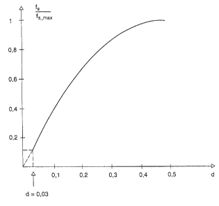
Figure 3 shows the profile of the ratio of the
operating frequency fs to be set to the
i
CA 02403053 2002-09-13
maximum switching frequency fs ma:~~ that is to
say the operating frequency for a pulse duty
factor d = 0.5, against the pulse duty factor
d.
Best mode for carrying out the invention
In an exemplary embodiment of the invention, the
operating frequency fs is set such that the operating
frequency is a maximum, that is to say fs = fs max, in a
case of maximum output power and thus of a maximum
pulse duty factor dmaX = 0.5. In the case of maximum
output power, the power transformer U therefore works
at optimum efficiency. If the output voltage, and thus
the output power, are reduced by reducing the pulse
duty factor d, the operating frequency fs is likewise
reduced, according to the invention. The operating
frequency f5 is only lowered in this case, however, so
far that saturation still does not arise in the power
transformer U.
The minimum permissible operating frequency fs,
normalized to the maximum operating frequency fsmax as a
function of the pulse duty factor d for which
saturation of the power transformer U still must not
occur, is yielded as:
fs =
fs_m..
This functional dependence is illustrated in figure 3.
As already mentioned, in this case fs maX is the maximum
operating frequency that is reached for a maximum pulse
duty factor dmax = 0.5, and in the case of which
saturation still does not occur during the maximum
i
CA 02403053 2002-09-13
_ g _
intermediate circuit voltage UzmaX. The above formula is
derived as follows:
The sum of the voltages across the coupling capacitors
Ckl, Ck2 Yields the intermediate circuit voltage Uz, and
s o Uckl + Uckz = Uz .
With reference to figure 2, the voltage-time areas A1
and A2 at the primary winding of the power transformer
L1 (in the steady state) are equally large, since only
alternating current flows through the coupling
capacitors Ckl, Ck2. It therefore holds that:
A1=Ul~t1=A2=U2~t2.
As already mentioned at the beginning, it holds further
that
d-tl; T=tl+t2; fs= 1. ~..
T T
One possibility of adapting the switching frequency fs
consists in reducing the operating frequency
continuously in such a way that the voltage-time area
at the power transformer U remains constantly at the
value ADes. Aoes can be selected in this case such that
the transformer U is operated with optimum efficiency
in conjunction with the maximum output power. However,
Apes can also be selected such that the power
transformer U is operated at the limit in relation to
saturation. The result in both cases is a profile
fs/fsmax according to the above formula, the
normalization frequency fsmax determining whether the
power transformer is operated at optimum efficiency or
at the limit in relation to saturation.
CA 02403053 2002-09-13
- 10 -
Another possibility of adapting the operating frequency
fs to the pulse duty factor d consists in lowering the
operating frequency fs in steps. If a specific value of
the pulse duty factor d is undershot when the output
power is reduced, the operating frequency fs is lowered
to the associated value. The adaptation of the
operating frequency fs can also be performed in such a
way that the profile according to the above equation is
approached by straight line segments, for example by
partial linearization.
The invention can be applied when implementing the
ballast with the aid of a half-bridge converter and
equally with the aid of a full-bridge converter.
The substantial reduction in the operating frequency
owing to the measure according to the invention may be
represented by an example:
Given a pulse duty factor of d = 0.03, which
corresponds to a dimming to approximately 1~ of the
maximum light flux, the above equation yields a
lowering of the operating frequency fs to 4 x 0.03 x (1-
0.03) X 100 = 11.6 of the maximum operating frequency
fsmax~ without the power transformer U going over into
the saturated mode. On the other hand, here the power
transformer can be operated with optimum efficiency
given a pulse duty factor d = 0.5, that is to say given
maximum output power (refer to a fixed intermediate
circuit voltage UZ).
The invention can be undertaken with the aid of a
microcontroller without additional outlay on circuitry,
or with the aid of a suitable analog or digital
circuit. In the case of alternative embodiments, it is
possible to carry out a normalization of the operating
frequency fs to other criteria as well, for example to
minimum losses in the transformer, or optimum thermal
conditions. It is to be taken into account in this case
i
CA 02403053 2002-09-13
- 11 -
that an optimum transformer utilization occurs near the
thermal limit thereof.
It can be sensible with regard to acoustic effects to
limit the ratio of f5 to fsmaX to a minimum of 0.4.