Note: Descriptions are shown in the official language in which they were submitted.
CA 02403167 2002-09-26
WO 01/82481 PCT/IB00/00509
METHOD AND APPARATUS FOR A OA'~~D OSCILT~ATO~.2. IN
DIGITAL CIRCUITS
BACK!CROUNT~ OF TIDE IN~VENTZON
The pz~esent invention relates to oscillators and more particularly to gated
oscillators.
Oscillators have a vride range of uses, For example, microprocessor
operation is synchronized by the periodic timing signals provided by an
oscillator.
Digital tachometers and digital speedometers in an automobile require a
precision
reference to provide accurate read-outs. Medical devices such as pacemakers
require an
accurate pulse generator to ensure proper rhythmic stimulation of the heart.
A gated oscillator is an oscillator that starts or stops oscillating by an
enabling signal_ In a conventional gated oscihatar, such as the on,e disclosed
in U.S. Pat.
No. 4,.365,? 12, oscillations are produced by periodically charging and
discharging a
capacitor bet~rr~en first and second voltage levels when the oscillator is
enabled. If it is
disabled, the oscillations are stopped by preventing the capacitor from
periodically
charging and discharging,
Let the first voltage level be lower than the second voltage level. Tf there
is no extra circuitry associated with the capacitor, then the capacitor will
continue to
discharge past the first voltage level toward the lower power supply ~roltaga
when the
oscillation is stopped. When the oscillator is enabled, a certain amount of
time is needed
to charge the capacitor from lower power supply voltage to the first voltage
level and then
to the second voltage level, whereupon oscillatory behavior ensues, The delay
ire
charging the capacitor from the lower power supply voltage to the first
voltage level
causes the first pulse in the pulse train to be wider than the rest of the
pulses. This error is
undesirable in applications which require and expect predictable pulse widths.
The error
can be substantially corrected if extra circuitry is added to prevent the
capacitor from
discharging past the first voltage level. This, of course, increases the
complexity of the
gated oscillator circuitry.
Gated oscillators have many applications in digital circuits. Zn an article
entitled "Gated oscillator emulates a tlig-flop," published in the March 1 b,
1995 issue of
EDN Magazine, a gated oscillator circuit is described in a flip-flop
configuration. Tn
another article entitled "Oscillator meets three requirements," published in
the December
CONFIRMATION COPY
CA 02403167 2002-09-26
WO 01/82481 PCT/IB00/00509
3, 1998 issue of ~D'bl Magaaine, a gated oscillator is described for use in
clock circuit as
the clocking source in a digital application.
A design that can be used as a gated oscillator is disclosed in U.S. Pat, No.
5,339,D53. A shmrtcoming oftb,is design, however, is that the enable signal
and the gated
oscillation are mixed at the circuit's output. Additional external circuitry
is therefore
required to separate the two signals,
A simplistic gated oscillator circuit can be built using an AND logic gate.
An enable signal is applied to on~c of its terminals and a continuous free
running oscillator
is applied to the other terminal, The output produces the desired gated
oscillations. This
prior art gated oscillator requires an external continuous free running
oscillator. A
problem with this design is the iry:ability of the enable sigaal to
synchronize with the free
running oscillator, thus producing indeterminate behavior, Another problem is
that the
free running oscillation fixes the frequency and duty cycle of the gated
oscillator output.
'X'et another is that the free running oscillator is continually running, even
when the
enable signal is removed. Consequently, there is unnecessary consumption of
power.
There is a need, therefore, far digital circuit design using a gated
oscillator
circuit which requires reduced support circuitry, It is desirable to provide a
design which
is energy efficient. There is a need for a design which can provide a tunable
ascillatiota
frequency. There is a frrrther for a design that can provide a tunable duty
cycle of the
oscillation. it is also desirable that the design has an ability to
synchronize the onset of
oscillatory behavior with the enable signal.
S'CY OF TIC 1NV,~NTION
A method for get,erating pulses in a digital circuit includes providing a
circuit hawing a variable operating point. The circuit is defined by a
transfer fraction
characterized by having an unstable operating region bounded by a first stable
operating
region and a second stable operating region, The circuit produces oscillatory
output when
its operating point is moved into the unstable region. The circuit produces a
non
oscillatory output when its operating point is placed into either ofthe first
and second
stable regions. The method further includes forcing the operating point into
the unstable
region to produce oscillatory output. 'fhe method further includes forcing the
operating
point into one of the stable regions in, order to terminate oscillations,
A gated oscillator circuit in accordance with the invention includes a
circuit having a transfer function defined by an unstable operating region
bounded by a
2
CA 02403167 2002-09-26
WO 01/82481 PCT/IB00/00509
first stable operating region and by a second stable operating region. The
transfer
function defines a set of operating points. The circuit is adapted to produce
oscillatory
output when the operating point is positioned in the unstable region. The
circuit is further
adapted to produce a rton-oscillatory output when its operating point is
positioned in
either of the first arid second stable regiaz~s. A function generator, which
selectively
produces an output of a Hxst level and an output of a second level is coupled
to the circuit
as an input signal. The operating paint is forced into the unstable region
when the
function generator output is at the f rst level. This level is called an
enable signal. The
operating point is forced into one of the stable regions when the function
generator output
1 Q is at its second output level. This level is referred to as a disable
signal.
Consequently, the ixtvention requires only the application of an enable
signal to enable oscillations or a disable signal to terminate oscillations.
The inventive
circuit is advantageous in that its oscillations start and stop substantially
instantaneously.
There axe no transients between the ON and OFF state of the oscillator.
Another
advantage is that the period of the first cycle of oscillation during an ON
period is the
same as the subsequent cycles ir< that ON period. There is no need for
additional
supporting circuit elements or special circuits fox maintaining standby levels
in the
capacitor. The circuit does not require any external free running oscillation.
The circuit
will generate its own oscillation.when triggered by the enable signal. The
circuit is
~0 inherently synchronized with the enable signal. Hy tuning the circuit
parameter, without
chaziging the cixcuit confZguration, the duty cycle and the frequency of
oscillation can be
'varied. The gated oscillation at the output of the circuit is not overlapping
with the enable
signal and therefore no additional circuit is required to separate them.
BRIEF DESCR1PTION OF THE T)rtAWxN'GS
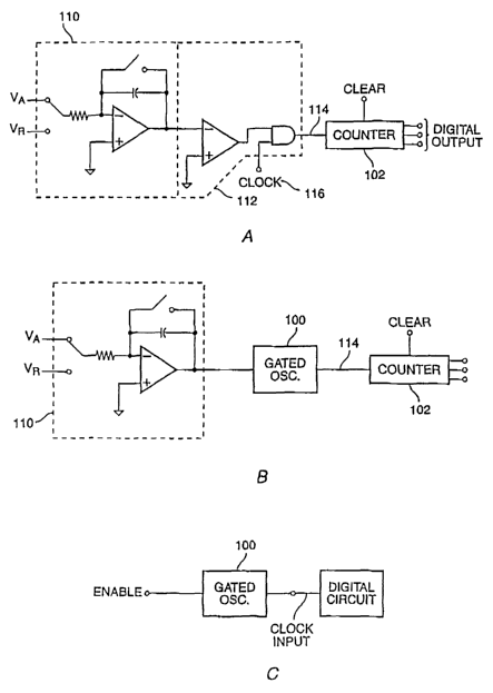
Figs. 1 A -1 C show hour the present invention obviates the need for a
clock in conventional clocked digital circuit designs.
Fig, 2 illustrates generally the transfer function of a circuit used in Figs.
lb
and 1 c.
Fig. 3 illustrates schematically a ciircuit arrangement for forcing the
operating point between stable and unstable regions.
Figs. 4 - 6 are examples of circuit configurations in accordance with the
inwentiori.
3
CA 02403167 2002-09-26
WO 01/82481 PCT/IB00/00509
Fig. 7 illustrates measurements taken from a circuit constructed in
accordance with the invention.
D1;SCRIPTION OF'TI~E SPECIFIC EMBODI~NTS
Referring to Fig. 1 A, a typical digital circuit such as the illustrated dual
slope analog-to-digital converter is shown, V~ is a referenced voltage and VA
is an
analog voltage to be converted to a digital representation. The output of
integrator 110 is
an analog waveform that contains inforaxiation of the amplitude of VA with
respect to V~.
A comparator that converts this analog waveform to an enable signal and AND
gate
combination 112 that receives an external clocking signal together produce a
gated
oscillation output 114 wlxich drives the counter.
Fig. 113 shows how a gated oscillator 100 inn accordance with the present
invention can be used to replace the conventional gated clock generation
circuit 1 I2 of
conventional digital circuits. As shown in Fig, 1C, generally, the clock input
ofmost
1 S conventional digital circuits can be driven by the gated oscillator
circuit of the present
invention. The discussion which follows will focus on the inventive
oscillator. It is
understood that digital circuits encompass a wide range of applications, The
invention is
therefore not limited to any one particular digital circuit. Rather, the
invention relates to
digital circuits having a clockloscillation generation function provided by
the cizcuit
disclosed hereinbelow.
Referring to Fig. 2, gated oscillator circuits in accordance rtrith the
present
invention exhibit a transfer function whose c~,~rve has a generally N-shaped
appearance.
For the purposes of tl~e present invention, the "transfer function" of a
circuit refers to tk~e
relationship between any two state variables of that circuit. For example,
electronic
circuits are typically characterized by their I-V curves, the two state
variables being
current (I) and voltage ('V). Such curves indicate how one state variable
(e.g., current, ~
changes as the other state variable (voltage, V) varies. As can be seen in
Fig. 2, a transfer
function curve 202 includes a portion which lies within a region 204, referred
to herein as
an "unstable" region. The unstable region is bounded on either side by regions
206 and
20$, each of which is herein referred to as the "stable" region. As can be
seen in Fig. 2,
portions of the transfer function curve 202 also lie in the stable regions.
A circuit in accozdance with the invention has an associated "operating
point" which is defined as its location on the transfer function 202. Fig. 2
shows three
operating point positions, 210, 210', and 210". 'The nature of the output of
the circuit
4
CA 02403167 2002-09-26
WO 01/82481 PCT/IB00/00509
depends on the location of the operating point along the transfer function. If
the operating
point is positioned along the portion 214 of the transfer function that lies
within region
204, the output of the circuit will exhibit an oscillatory behavior. Hence,
the region 204
in which this portion of the transfer function is found is referred to as an
unstable region.
If the operating point is positioned along the portions 216, 218 of the
transfer function
that lie within either of regions 206 and 208, the output of the circuit will
exhibit a
generally time-varying but otherwise non-oscillatory behavior. For this
reason, regions
206 and 208 are referred to as stable regions.
Referring to Figs. 2 and 3, a general configuration for varying floe
operating point of a circuit is shown. The figure shows a circuit 302 hawing
an input
defined by terminals 303 and 305. An inductive element 304 is coupled to
terminal 305.
A function generator 310 is coupled beiween the other end of inducti~re
element 304 and
terminal 303 of circuit 302, thus completing the circuit. Itt accordance with
the izwention,
circuit 302 has a transfer function which appears N-shaped. Further in
accordance with
the invention, circuit 302 is characterized in that its operating point can
moved into and
out of the unstable region 204 depending on the level of the output Vs of
function
generator 310. This action controls the onset of oscillatory behavior, and
cessation of
such oscillatory behavior, at the output Vo"t of circuit 302. Forcing the
operation point to
be on a portion of the transfer function that lies in the unstable region 204
will result in
oscillatory behavior. Forcing the operating point to lie orx the transfer
fmzction found in
one of the stable regions 206, 208 will result in non-oscillatory behavior.
An exannple of a circuit that eXhibits the N-shaped transfer function, is ax1
operation amplifier (op-amp) configured with a feedback resistor between the
op-amp
output and its non-inverting input. Fig. 4 shows such a circuit 400.. An op-
amp 402
2~ includes a positive feedback path wherein the op-amp's output Vou~ feeds
back to its non-
inverting input via feedback resistor 408 having a resistance Rf. A portion of
the output
voltage of op-amp 402 is provided to its inverting input. Fig, 4 shows a
voltage dividing
circuit comprising resistors 404 and 406, having respectively resistances R~
and R2, to
supply a portion of the op-arnp output back to its inverting input. Completing
the circuit
is an inductor 410 and function generator 310 coupled in series between the
non-inverting
input of op-an~;p 402 and ground. A typical off the-shelf op-amp can be used,
such as the
commonly available LM-358 op-amp.
Another example of a circuit having an N shaped transfer function is
shown in Fig. S. Here, circuit 500 comprises a tunnel diode 502 coupled to
function
S
CA 02403167 2002-09-26
WO 01/82481 PCT/IB00/00509
generator 314 through inductive element 410. The outlrut Yo"~ 15 taken across
resistor
504, which is coupled between the other end of diode 502 and ground.
The foregoing circuits can be expressed by the following generalized pair
of coupled equations which describe a two-variable Van der Pol (VdP)
oscillator:
L d = f (t)-x (1 )
~ ~ =Y-'1'(x) (2)
where x and y are the state variables of the VdP oscillator,
~ and s are parameters of the Vdl' oscillator,
,~'(t) is a time varying Forcing function that is controllable and can be used
to move
the operating point of the Vdp oscillator, and
'E(x) is a cubic funetioz~ of variable x. '~(x) is the key for establishing a
1 S controllable VdP oscillator.
Equations (1) and (2) relate to the circuit ofFig. 4 by replacing variables x
andy respectively with Yand l to represent physical variables that are
commonly used in
a circuit design. Hence,
L dt =Y, -Y
~mC ~~ =i-~(Y) ,(4)
1?arameter C in Eq, (4) represents a small parasitic capacitor 420 across the
voltage Y, shown in Fig. 4 by phantom lines. Y~ is the time varying voltage
source of
function generator 3 LO which acts as forcing function. 'the operating point
of circuit X00
is obtained by setting dV = 0 and al ' 0. Equations (3) and (4) become Y' = YS
and l
dt dt
~I'(1'), respectively, l = ~~'(V) is the transfer function vfthe op amp with
lZf, Rj and R2
combinations. Thus, with reference back to Fig. 2, it can be seen that
transfer fraction
curve 202 is defined by l = '1'(f~.
The intersection between the lire Y ~ Y~ and the curve l .= Y'(Y) defines
the operating point 210 ofthe circuit. A closer inspection oftransfer function
202 defined
by t = ~(Y) reveals that segments 216, 218 lave positive slope (dildY~ 0) and
segment
6
CA 02403167 2002-09-26
WO 01/82481 PCT/IB00/00509
214 has a negative slope (dild~'< 0). When op-amp 402 (Fig. 4) is saturated,
operating
point 210 lies along one of the two positive sloped segments 21b, 218. When op-
amp 402
is operating linearly, the operating point lies along the negative sloped
segment. When
the operating point is on the negative sloped segment 214, oscillatory
behavior will be
observed at the output Vo", of circuit 400. Fence the negative sloped segment
is said to
lie in unstable region 204 as is operating point 210. When the operating paint
210', 210"
is on a positive sloped segment, a non-oscillatory output is observed. Hence
the positive
segments are said to lie in stable regions 206, 208,
The operating point 210 can be moved along the transfer function, by
changing the output V'$ of function generator 310 as it is applied to the
input o~ circuit
400. In particular, the operating point can be moved into unstable region 204
when an
enable signal is provided by the fw~ction generator. ironversely, the
operating point can
be moved out of the unstable region and into one of the stable regions 206,
208 by the
application of a disable signal, The resulting behavior of circuit 400 is that
of a gated
oscillator.
Fig, 6 shows yet another embodiment of the gated oscillator of the
invention. As in the foregoing figures, a function generator 3I0 provide a
variable
voltage signal Y$. This signal feeds through inductor 410 into a first
inventor 602, The
output of inverter 602 is coupled to a secarcd inverter 604, The output of
inverter 604 is
taken across resistor 60S to provide output Vo"c. A feedbacl~ path from the
output of
inverter 604 to the input of inverter 602 is provided via resistor 606.
Referring now to Fig. 7, an oscilloscope trace is shown, illustrating the
foregoing described behavior. Trace 1 is the output V$ of function generator
310 as
applied to the input of circuit 400. A first portion of the trace constitutes
the LNA,BLE
signal. This is followed by a second portion which constitutes the DISABL)J
signal.
Preferably, the function generator output is a digital vvaveforno, For
example, a typical
digital waveform is a square wave such as shown in Fig. 7, rt is noted that
typically, the
digital waveform will be asymmetric along the time axis, since the periods of
ON time
and OFF time will depend on the nature of the particular application of the
gated
oscillator.
Trace 2 is the output voltage Va"~ of circuit 400. A~s can be seen, the
circuit begins to oscillate when an enable signal is received. The
oscillations continue for
the duration of the enable signal. It can be further seen that the first
period x~ of the first
7
CA 02403167 2002-09-26
WO 01/82481 PCT/IB00/00509
cycle has the same duration as each of the remaining cycles, Tz. The pulse
width can be
varied by changing the circuit parameters Rr, R~, and 1Z2 or the op-amp I3C
bias V~.
'When the disable signal is receued, the circuit stops oscillating
instantaneously.
The location of the operating point along the transfer curve in the unstable
region affects the period of oscillations of the output of circuit 400. The
location of the
operating point within the unstable region (and the stable regions for that
matter) can be
determined by adjusting the level of the forcing function, It can be seen,
therefore, that
different oscillation periods can be attained from circuit 400 by applying an
enable signal
of different levels. The gated oscillator of the invention can thus be made to
produce
different pulse widths by the use of a function generator in which the level
of the enable
signal can be controlled.
The invention described herein uses an unconventional method of
controlling the operating point of a "VdP oscillator to pzvvide a
significantly simplified
digital circuit desigrw which obviates the need for a clock circuit. The
inventive circuit
does not need additional supporting components. The invention obviates the
need for a
charging and a discharging capacitor for generating pulses. The invention
dispenses with
the support circuitry conventionally required to maintain capacitor potential
when
oscillation is stopped.
The invention requires only that an enabling signal be provided to "force"
the V'dp oscillator to oscillate and a disabling signal to stop oscillations.
These signals
oan be readily generated by any of a number of Irnoum circuit designs.
The inventive gated oscillator Circuit is advantageous in that its
oscillations
start and stop substantially instantaneously. Consequently, there are no
transients
between the ON and OFF state of the oscillator. Another advantage is that the
period of
the 1-irst cycle of oscillation during an ON period is the same as the
subsequent cycles
during that ON period.
Another advantage is that the circuit does not require any external free
running oscillator. The circuit will generate its own oscillations when
triggered by an
enable signal. Consequently, tk~is shows for sagni~caz~t reductions in power
consumption
in digital circuit applications. This is especially advantageous given the low
povuer
requirements of many of today°s digital applications,
Yet azo,other advantage, the circuit is inherently synchronized with the
enable signal. By tuning the circuzt parameter, ~svathout changing the circuit
configuration, the duty cycle and the frequency of oscillation can be varied.
The gated
8
CA 02403167 2002-09-26
WO 01/82481 PCT/IB00/00509
oscillation at the output of the circuit does not overlap with the enable
signal and
therefore no additional circuitry is required to separate the signals, thus
realizing a
simplification in the gated oscillator circuitry,
9