Note: Descriptions are shown in the official language in which they were submitted.
CA 02403427 2002-09-17
WO 01/71322 PCT/CA01/00367
METHOD AND APPARATUS FOR ASSAY FOR MULTIPLE ANALYTES
FIELD OF THE INVENTION
The present invention relates to a method and apparatus for detecting
multiple analytes in a medium, and more particularly the present invention
relates
to a method of assaying based on light diffraction which appears or changes
upon the binding of analytes to their specific receptors laid out in patterns
on a
substrate.
BACKGROUND OF THE INVENTION
In many instances, it is desirable to determine the presence and the
amount of a specific material in solution (the 'medium'). Surface-based assays
rely on the interaction of the material to be assayed (the 'analyte') with a
surface
that results in a detectable change in any measurable property. For the
purpose
of this patent application, the term 'analyte' refers to the material to be
assayed.
Examples of analytes include: an ion; a small molecule; a large molecule or a
collection of large molecules such as a protein or DNA; a cell or a collection
of
cells; an organism such as a bacterium or virus. Analyte-specific receptor, or
'recognition element' refers to that complementary element that will
preferentially
bind its partner analyte. This could include: a molecule or collection of
molecules;
a biomolecule or collection of biomolecu. les, such as a protein or DNA; a
groove
on the substrate that has the complementary geometry and/or interaction. In
general, in order to assay for a specific analyte, the surface is modified so
as to
offer the appropriate chemical interaction. In immunoassays, for example, one
takes advantage of the specificity of the antibody-antigen interaction: A
surface
can be coated with an antigen in order to assay for the presence of its
corresponding antibody in the solution. Similarly, a strand of
deoxyribonucleic
= acid (DNA) can be attached to a substrate and used to detect the presence of
its
complementary strand in solution. In any of these cases, the occurrence of
binding of the analyte to its recognition element on the surface, which thus
identifies the presence of the specific analyte in solution, is accompanied by
1
CA 02403427 2002-09-17
WO 01/71322 PCT/CA01/00367
detectable change. For example, the binding can produce a change in the index
of refraction at the interfacial layer; this can be detected by ellipsometry
or
surface plasmon resonance. Alternatively, the bound analyte molecules may emit
light; this emission can be collected and detected, as is the case for
fluorescence-based sensors. Non-optical signals may also be used, as in the
case of radio immunoassays and acoustic wave sensing devices.
Diffraction is a phenomenon that occurs due to the wave nature of light.
When light hits an edge or passes through a small aperture, it is scattered in
different directions. But light waves can interfere to add (constructively)
and
subtract (destructively) from each other, so that if light hits a non-random
pattern
of obstacles, the subsequent constructive and destructive interference will
result
in a clear and distinct diffraction pattern. A specific example is that of a
diffraction
grating, which is of uniformly spaced lines, typically prepared by ruling
straight,
parallel grooves on a surface. Light incident on such a surface produces a
pattern of evenly spaced spots of high light intensity. This is called Bragg
scattering, and the distance between spots (or 'Bragg scattering peaks') is a
unique function of the diffraction pattern and the wavelength of the light
source.
There is a unique correspondence between a pattern and its diffraction image,
although in practice, diffraction is best illustrated by using periodic
patterns,
because these yield easily recognized diffraction images of clearly defined
regions of high and low light intensity.
Diffraction techniques are commonly used in studies of molecular
structurp; specifically, X-ray diffraction is used in the identification of
chemical
compounds and in the determination of protein structures. However, the
principle
of diffraction, especially in the optical domain, has rarely been invoked for
use in
assays.
United States Patent No. 4,647,544 (Immunoassay using optical
interference detection) describes a light optical apparatus and method, in
which a
ligand, or an antibody, is arranged in a predetermined pattern, preferably
stripes,
on a substrate, and the binding between ligand and antiligand, or between an
antibody and an antigen, is detected by an optical detector set at the Bragg
2
CA 02403427 2002-09-17
WO 01/71322 PCT/CA01/00367
scattering angle, which is expected to arise due to optical interference. The
pattern of ligand or antibody is created by first laying out a uniform layer
of
antibody on a substrate, then deactivating sections of this coverage.
United States Patent No. 4,876,208 (Diffraction immunoassay apparatus
and method) describes the apparatus and reagents for an immunoassay based
on a silicon or polysilicon substrate with a pattern of evenly spaced lines of
a
biological probe (a 'biological diffraction grating') to which binding can
take place.
The pattern is created by first coating the substrate with an even layer of
antibodies, then deactivating regions by the use of a mask and of ultraviolet
(UV)
lights. This idea is extended to the assay of DNA in United States Patent No.
5,089,387 (DNA probe diffraction assay and reagents), which describes a
biological diffraction grating, and a process for its manufacture by first
immobilizing a uniform layer of hybridizing agent on a smooth surface, and
then
exposing this surface to UV radiation through a mask with diffraction grating
lines. The UV exposure deactivates the hybridizing agent, leaving a pattern of
lines of active hybridizing agents.
The above patents on assays by diffraction are necessarily restricted to
the case of a single analyte. In United States Patent Nos. 4,876,208 and
5,089,387, the described techniques are extended to the case of multiple
analytes by making biogratings with identical patterns of different analyte-
specific
receptors on different areas of a substrate and then measuring the diffraction
due
to each pattern measured independently of the others.
United States Patent No. 5,922,550 (Biosensing devices which produce
diffraction images) describes a device and method for detecting and
quantifying
analytes in a medium based on having a predetermined pattern of self-
assembling monolayer with receptors on a polymer film coated with metal. The
size of the analytes are of the same order as the wavelength of transmitted
light,
thereby its binding results in a diffraction pattern that is visible. This
patent also
describes a method of producing the patterned surface by microcontact printing
of the self-assembled monolayer of receptors on a metal-coated polymer. This
is
extended to the case of a predetermined pattern of receptors (not necessarily
3
CA 02403427 2002-09-17
WO 01/71322 PCT/CA01/00367
self-assembling) in United States Patent No. 6,060,256 (Optical Diffraction
Biosensor). The technique of rnicrocontact printing of self-assembled
monolayers
on a metal substrate is described in United States Patent No. 5,512,131
(Formation of microstamped patterns on surfaces and derivative articles).
Microcontact printing is a technique of forming patterns of micrometer
dimensions on a surface using an elastomeric stamp; the material to be
patterned serves as the "ink" and is transferred by contacting the stamp to
the
surface. Microcontact printing of proteins on silicon, silicon dioxide,
polystyrene,
glass and silanized glass is reported in Bernard, A; Delamarche, E.; Schmid,
H.;
Michel, B.; Bosshard, H.R.; Biebuyck, H.; "Printing Patterns Of Proteins"
Langmuir (1998), 14, 2225-2229.
To utilize diffraction techniques in surface-based assays, it is important to
be able to produce a material patterned with receptors, and the five patents
discussed above have outlined their ways of doing so. In addition, other
techniques that exist in the literature may be adaptable for patterning. For
example, using photolithographic techniques, oligonucleotides have been
immobilized on a substrate in arrays such that each array is a distinct
species.
United States Patent Nos. 5,831,070 and 5,599,695 show how this is done
through the use of deprotection agents in the gas phase. This approach has not
been used in the creation of patterns for diffraction assays, but can be
adapted
for such with the design of an appropriate mask.
It would be very advantageous to provide a method of simultaneously
assaying for multiple analytes using diffraction of light.
SUMMARY OF THE INVENTION
An objective of the present invention is to provide a method for the
simultaneous assay of multiple analytes using diffraction of light.
In accordance with this objective the present invention provides a method
for detecting multiple analytes in a medium. The method involves the laying
down
of analyte-specific receptors on the surface of a solid substrate, such that
each
type of receptor defines a distinct pattern. Exposure of the substrate to a
medium
4
CA 02403427 2010-02-03
containing one or more analytes will result in binding events between each
analyte and its analyte-specific receptor. These binding events will result in
a
diffraction image from which can be derived the presence of the analyte(s).
In one aspect of the invention there is provided a sensing element for
use in a light diffraction assay for detecting the presence or absence of at
least two analytes, comprising:
a substrate including a surface and on said surface a first pre-selected
pattern of first analyte-specific receptors and at least a second pre-selected
pattern including second analyte-specific receptors, wherein each of said pre-
selected patterns on said surface is distinct from the other pre-selected
pattern of analyte-specific receptors formed on the surface,
wherein said surface includes a selected area that is illuminated by an
incident beam, and both the first pre-selected pattern and the at least second
pre-selected pattern are contained in said selected area such that each
analyte-specific receptor pattern within the selected area is simultaneously
illuminated and, when bound to an analyte, gives rise to a pre-selected
diffraction pattern distinct from diffraction patterns formed from all other
unbound and bound pre-selected patterns on the selected area of the surface.
In another aspect of the invention there is provided a method for
detecting simultaneously at least two analytes in a medium using light
diffraction, comprising:
providing a substrate including a surface and on said surface a first
pre-selected pattern of first analyte-specific receptors and at least a second
pre-selected pattern including second analyte-specific receptors, wherein
each of said pre-selected patterns on said surface is distinct from the other
pre-selected pattern of analyte-specific receptors formed on the surface, and
when bound to an analyte, gives rise to a pre-selected diffraction pattern
distinct from diffraction patterns formed from all other unbound and bound
pre-selected patterns on the surface;
contacting said surface of said substrate with said medium for a
sufficient time to permit analytes present in said medium to bind to their
associated analyte-specific receptors; and
5
CA 02403427 2010-02-03
illuminating said substrate and detecting, at a position spaced from the
substrate surface, an image of diffracted light from said substrate surface
and
analysing the image of diffracted light for the presence or absence of each of
said pre-selected diffraction patterns representative of binding of said
analytes
to their associated analyte-specific receptors and identifying from the image
of
diffracted light the presence or absence of said analytes in said medium.
In this aspect of the invention illuminating the substrate may include
illuminating a sufficient area of the substrate to illuminate at least a part
or all
of each of the at least two patterns. Alternatively, illuminating the
substrate
may include illuminating the patterns one a time.
In another aspect of the invention there is provided an apparatus for
detection of analytes in a medium using diffraction of light, comprising:
a source of illumination;
a sensing element including a substrate having a surface and on said
surface a first pre-selected pattern of first analyte-specific receptors and
at
least a second pre-selected pattern including second analyte-specific
receptors, wherein each of said pre-selected patterns on said surface is
distinct from the other pre-selected pattern of analyte-specific receptors
formed on the surface, wherein said surface includes a selected area that is
illuminated by an incident beam, and both the first pre-selected pattern and
the at least second pre-selected pattern are contained in said selected area
such that each analyte-specific receptor pattern within the same selected area
is simultaneously illuminated and, when bound to an analyte, gives rise to a
pre-selected diffraction pattern distinct from diffraction patterns formed
from
all other unbound and bound pre-selected patterns on the selected area of the
surface, said source of illumination being positioned so as to illuminate said
selected area of substrate surface;
detection means positioned with respect to said sensing element to
detect at a position spaced from the substrate surface, an image of diffracted
light from the substrate surface; and
processing means for analysing said image of diffracted light for
presence of each of said pre-selected diffraction patterns representative of
6
CA 02403427 2010-02-03
binding of one or more analytes to their associated pre-selected analyte-
specific receptors.
The sensing element substrate may be transparent and have two
opposed surfaces upon which analyte-specific receptors are patterned. The
assay is performed by contacting both faces of the substrate with the medium,
for example, by dipping.
In another aspect of the invention there is provided a method of
producing a sensing element for use in a light diffraction assay, comprising:
providing a substrate including a surface, wherein said surface includes
a selected area that is illuminated by an incident beam;
depositing within the selected area on the surface of the substrate a
first pre-selected pattern of first analyte-specific receptors and at least a
second pre-selected pattern including second analyte-specific receptors such
that each analyte-specific receptor pattern within the same selected area is
simultaneously illuminated, wherein each of said pre-selected patterns on said
selected area is distinct from the other pre-selected pattern of analyte-
specific
receptors formed on the selected area of the surface and, when bound to an
analyte, gives rise to a pre-selected diffraction pattern distinct from
diffraction
patterns formed from all other unbound and bound pre-selected patterns on
the selected area of the surface.
In another aspect of the invention there is provided a method for
detecting simultaneously at least two analytes in a medium using light
diffraction, comprising:
providing a substrate including a surface comprising glass, mica,
polished silicon, silicon dioxide, a polymeric material, or a substantially
transparent polymeric material, and on said surface a first pre-selected
pattern of a first analyte-specific receptors and at least a second pre-
selected
pattern including second analyte-specific receptors, wherein each pre-
selected pattern, when bound to an analyte, gives rise to a pre-selected-
diffraction pattern distinct from diffraction patterns formed from all other
unbound and bound pre-selected patterns on the surface;
contacting said surface of said substrate with said medium for a
6a
CA 02403427 2010-02-03
sufficient time to permit analytes present in said medium to bind to their
associated analyte-specific receptors; and
illuminating the substrate and detecting, at a position spaced from the.
substrate surface, an image of diffracted light from said substrate surface
and
analyzing the image of diffracted light for presence or absence of each of
said
pre-selected diffraction patterns representative of binding said analytes to
their associated analyte-specific receptors and identifying from the image of
diffracted light the presence or absence of said analytes in said medium.
In another aspect of the invention there is provided a method for
detecting simultaneously at least two analytes in a medium using light
diffraction, comprising:
providing a substantially transparent substrate including a surface and
on said surface a first pre-selected pattern of first analyte-specific
receptors
and at least a second pre-selected pattern including second analyte-specific
receptors, wherein each of said pre-selected patterns on said surface is
distinct and, when bound to an analyte, gives rise to a pre-selected
diffraction
pattern distinct from diffraction patterns formed from all other unbound and
bound pre-selected patterns on the surface;
contacting said surface of said substrate with said medium for a
sufficient time to permit analytes present in said medium to bind to their
associated analyte-specific receptors; and
illuminating said substrate and detecting, at a position spaced from the
substrate surface, an image of diffracted light from said substrate surface
and
analysing the image of diffracted light for the presence or absence of each of
said pre-selected diffraction patterns representative of binding of said
analytes
to their associated analyte-specific receptors and identifying from the image
of
diffracted light the presence or absence of said analytes in said medium,
wherein said surface is illuminated from one side of said substrate, and
wherein said light diffracted from said substrate is detected on the opposite
side of said substrate.
6b
CA 02403427 2010-02-03
BRIEF DESCRIPTION OF THE DRAWINGS
The invention will now be described, by way of example only, reference
being had to the accompanying drawings, in which;
Figure 1a is a top view of a sensing element for a diffraction assay for
detecting two or more analytes having three patterns of analyte-specific
receptors with the three patterns interleaved in the same area on the
substrate surface;
Figure lb is a top view of a sensing element for a diffraction assay for
detecting two or more analytes having three patterns of analyte-specific
receptors with the three patterns spaced from each other on the substrate
surface;
Figure 2a shows a diagrammatic illustration of an apparatus for
performing an assay in accordance with the present invention using a
transmission configuration;
Figure 2b shows a diagrammatic illustration of an apparatus for
performing
6c
CA 02403427 2002-09-17
WO 01/71322 PCT/CA01/00367
an assay using a reflection configuration;
Figure 2c shows a diagrammatic illustration of an apparatus for performing
an assay using a configuration with a rotating mirror to direct the signal to
a
detector;
Figure 3a is a perspective view of a cell for performing an assay in the
static mode;
Figure 3b is a cross-sectional view showing an embodiment of a flow cell
constructed for performing the present assay;
Figure 3c is a perspective view of an alternative embodiment of a flow cell
constructed in accordance with the present invention;
Figure 3d is a cross-sectional view of a flow cell using total internal
reflection;
Figure 4 shows a glass substrate patterned with goat immunoglobulin G
(IgG) by microcontact printing, visualized by atomic force microscopy;
Figure 5 shows a glass substrate patterned with goat IgG and rabbit IgG
produced by microcontact printing using a stamp for both having the same
pattern but rotated -90 with respect to each other, the images being obtained
by
atomic force microscopy.
Figure 6 shows a glass substrate patterned with mouse IgG and rabbit IgG
produced by microcontact printing using a stamp for both having the same =
pattern but rotated -30 with respect to each other, the images being obtained
by
atomic force microscopy;
Figure 7 shows effect of treating a rabbit and mouse IgG cross-stamped
substrate sequentially with the indicated solutions;
Figure 8 shows effect of treating a biotin and fluorescein (both as bovin
serum albumin (BSA) conjugates) cross-stamped substrate sequentially with the
indicated solutions;
Figure 9 shows the use of an avidin stamped substrate for the detection of
single-stranded DNA by the sequential treatment with the indicated solutions;
Figure 10 shows the titration of a substrate patterned with rabbit IgG with
increasing concentrations of anti-rabbit IgG; and
7
CA 02403427 2006-03-22
Figure 11 shows the change in signal over time resulting from the
treatment of a biotin-BSA patterned substrate with streptavidin solution
DETAILED DESCRIPTION OF THE INVENTION
The present invention provides a method for the assay of multiple analytes
on the same general region of a substrate using light diffraction. The method
takes advantage of the unique correspondence between a given receptor pattern
and its diffraction pattern, in order to assess the presence or absence of
specific
analytes. Analyte-specific receptors are laid out on the surface of a solid
substrate, either directly or through an intervening layer, such that each
type of
receptor defines a unique pattern. For the purpose of this patent, two
patterns
are considered 'distinct' or 'unique' if they correspond to diffraction
patterns
distinguishable from each other. The solid substrate may be transparent,
partially
transparent, or reflecting at the wavelength of the incident illumination. In
the
case of a transparent substrate, analyte-specific receptors may be patterned
on
one or both surfaces of the substrate.
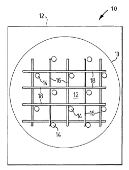
Figures la and lb depict general representations of two possible layouts
of patterns of recognition elements on a substrate. Referring to Figure la, a
sensing element shown generally at 10 comprises a substrate 12 that holds
multiple recognition elements, in this example there are three different
recognition elements 14, 16 and 18, with each recognition element laid out in
a
unique pattern on the surface of the substrate. In this embodiment the
patterns
14, 16 and 18 interpenetrate each other in a preselected area of the substrate
12. Under illumination, defined by the circle 13, portions of the different
patterns
within circle 13 are simultaneously illuminated. Figure lb shows another
sensing
element 20 having a substrate 12' having three different analyte-specific
receptors laid out in three different unique patterns 21, 23 and 25 distinct
from
each other but in this case the patterns do not interpenetrate each other.
Once the recognition element that is capable of specific binding (e.g.,
protein, oligonucleotide, antibody, etc.) is laid out on the surface in a
preselected
pattern, the medium to be assayed is contacted with the substrate, allowing
8
CA 02403427 2002-09-17
WO 01/71322 PCT/CA01/00367
analytes present in the medium to bind to their complementary recognition
element. When a particular analyte is present in the medium, the subsequent
binding event between analyte and its complementary recognition element is
accompanied by a change in the local thickness of the layer on the substrate
and/or in the local index of refraction. Both the change in thickness and the
change in index of refraction will alter the optical properties at the
interface
between the substrate and medium in regions where the binding has taken place.
Since the recognition elements are present on the substrate in a predetermined
pattern, light incident on the substrate will not be scattered uniformly, but
rather
will be diffracted. In one embodiment of this invention, the patterned
substrate is
non-diffracting, and the binding events result in an observable diffraction
image.
In another embodiment, the patterned substrate itself produces an observable
diffraction image, but the binding events alter the intensities of the
diffracted
signal.
The pattern of the diffracted light (the 'diffraction image') corresponds to a
unique pattern on the substrate. The assay works in the following manner: The
substrate is patterned with a multipilicity of analyte-specific receptors, say
RA,
RB, RC, such that each type of receptor defines a distinct pattern, PA, PB,
PC,
respectively. (Patterns are considered distinct if they individually
correspond to
distinguishable diffraction images, say DA, DB, DC respectively). In the case
of
only one type of analyte present, say AA which is complementary to receptor
RA,
said analyte will bind to its partner and the pattern corresponding to that of
receptor RA will thus be highlighted by a change in refractive index and/or
height
above the substrate due to this binding event. If the patterned substrate is
initially
non-diffracting, the binding event will cause the appearance of a diffraction
image
that looks like DA. Thus, observing a diffraction image that looks like DA
immediately identifies the presence of analyte AA bound to receptor RA, and
hence the presence of AA in the original medium. The signal intensities at the
bright regions (for example, the Bragg peaks if the pattern were a grating)
reflect
the amount of binding, and can be calibrated in order to effect quantification
of
bound analytes, and thus makes for a quantitative assay. If there are a
9
CA 02403427 2002-09-17
WO 01/71322 PCT/CA01/00367
multiplicity of analytes present, say AA, AB, AC, complementary partners to
RA,
RB, RC respectively, the binding events will produce a diffraction image that
is a
non-additive composite of DA, DB and DC. That is, patterns DA, DB and DC will
be present in the observed diffraction image, but additional features will
also be
present. In this case, the assay can be effected in either of following
manner. (1)
The full diffraction image can be stored on a computer; and with the use of
image
processing and computational tools, the image is deconvoluted into the
individual
patterns. (2) In a preferred embodiment of this invention, the appearance or
change in signal at specific regions of the diffraction image signify the
presence
of specific analytes. For example, the appearance of a bright region
characteristic of DA but not DB or DC is a good marker for the presence of AA.
Similar regions can be located for AB and AC, and when electronic detection is
employed, their signal intensities can be calibrated (as in the case of only
one
analyte) in order to effect a quantitative assay. The more analytes and
analyte-
specific receptor patterns present, the more complex the observed diffraction
image will be. It is thus important to choose patterns that are as distinct
from
each other as possible to enable ease of assay. As well, in simple cases,
visual
inspection may suffice to indicate distinctness of patterns; that is, one can
clearly
see that the diffraction image corresponds to DA and not DB. However, as
complexity increases, a preferred embodiment of this invention uses an imaging
device that will enable a more effective comparison. In one embodiment, the
detector obtains the diffraction image as an electronic signal that is stored
in a
computer, and image processing is utilized. In another embodiment, information
is already stored in the computer that will facilitate such interpretation.
For
example, changes in intensities at specific pixels of the image signify a
particular
binding event. In this latter case, this information may either be programmed
in
the computer or encoded in the substrate itself and be read by the apparatus
during the assay.
Referring to Figure 2a, an apparatus for performing an assay in
accordance with the present invention is shown generally at 30. Apparatus 30
is
configured for transmission and comprises a source of illumination 32,
substrate
10
CA 02403427 2002-09-17
WO 01/71322 PCT/CA01/00367
with the patterned recognition elements located on a surface thereof, and a
detector 34 for detecting the light after it has been transmitted through the
substrate. Figure 2b illustrates another embodiment of an apparatus at 40
constructed in accordance with the present invention that is configured for
5 operating in reflection mode. Figure 2c illustrates another embodiment of
an
apparatus 50 for use in the transmission mode including a rotating mirror 11
to
direct the signal transmitted through substrate 10 to detector 34. A
similar.design
may be used in another embodiment of a reflection configuration.
Light source 32 may produce a monochromatic beam, typically light with a
10 wavelength in the range from the ultraviolet to the infrared, but
preferably a
coherent and collimated light beam, such as would come from a laser (e.g.
diode,
He-Ne, Nd:YV04, Argon-ion). This may be a low power, continuous wave laser.
The substrate 10 may either be an optically transmitting or partially
transmitting
substrate with respect to the wavelength of light used in Figure 2a or it may
be
reflecting or partially reflecting as shown in Figures 2b and 2c. In one
embodiment of this invention, the incident illumination is delivered to the
substrate by an optical fibre. In another embodiment of the invention, the
incident
illumination is scanned (rastered) over the substrate, illuminating one or
more
recognition elements at a time. Since each pattern is distinct and it is known
a
priori which analyte binds with that pattern, a detection of a change in
diffraction
image associated with that pattern immediately identifies the presence of that
analyte.
The substrate is preferably flat or smooth enough so that impinging light
will not be scattered to such an extent that it obscures or degrades the
diffraction
signal. Non-limiting examples of substrates that may be used are glass, mica,
polished silicon, silicon dioxide, various smooth polymer materials, gold and
other metals with reflecting surfaces, either as sheet or as thin films on a
support.
The substrate may be of any size, but the area of the active region, that
which
contains the patterns of analyte-specific receptors or recognition elements,
should be at least the cross sectional size of the incident beam as it
intercepts
the surface of the substrate, and preferably of comparable size (indicated by
the
11
CA 02403427 2002-09-17
WO 01/71322 PCT/CA01/00367
circles 13 in Figures la and 1b). In this way each analyte-specific receptor
pattern is simultaneously illuminated so that the resulting diffraction image
simultaneously gives information about the presence or absence of two or more
analytes depending on the number of analyte-specific receptor patterns in the
illuminated portion of the substrate.
In applications in which moisture may be problematic, the substrate may
be placed in a cell that is partially evacuated in order to reduce moisture.
This is
advantageous where it is desirable to reduce the signal strength that may
arise
due to water condensation. However, in the case where the analytes but not
their
partner receptors are favoured by water, the presence of water condensation
(also called 'condensation figures') can be utilized to enhance the diffracted
signal. In another embodiment of the invention, the assay may also be
performed in situ by placing the substrate into a chamber into which the
medium
can be introduced. Figure 3a shows a cell 50 with a substrate 52 immersed in a
liquid being tested for the presence of one or more of the analytes in a
static
configuration with no flow-through. Analyte-specific receptors are patterned
on
one or both surfaces of substrate 52.
Figure 3b shows a flow configuration comprising a cell 56 comprising
spaced parallel walls 58 and 60 with analyte-specific receptor patterns formed
on
the insides of each of the walls. The liquid is continuously flowed through
the cell
during operation and the reflection or transmission mode may be used as
indicated by the arrows. Figure 3c shows another embodiment of a flow cell 66
comprising spaced parallel walls 68 and 70 with wall 70 having an inlet port
72
and an outlet port 74. The analyte specific receptor pattern 76 is formed on
the
inner surface of wall 68 and an 0-ring 78 is used to seal the flow chamber. In
each of these embodiments the chamber should have at least one window
transparent to the incident illumination. The substrate within the chamber is
located in direct line of illumination, and the assay is performed either in
reflection or transmission, as described previously. In another embodiment,
the
fluid chamber may comprise the patterned substrate as one or more of its
windows. In these embodiments, the time dependence of the binding events may
12
CA 02403427 2002-09-17
WO 01/71322
PCT/CA01/00367
be monitored simultaneously for all analytes. This may be useful for
measurement of relative binding affinities.
Detector 34 must be sensitive to the illumination of choice. The detector
34 may be a position sensitive photodiode, a photomultiplier tube (PMT), a
photodiode (PD), an avalanche photodiode (APD), a charged-coupled device
(CCD) array, the unaided eye, a camera, a photographic plate, or any other
imaging device. In one embodiment of this invention, the transmitted or
reflected
signal is collected by an imaging optical fibre and directed to an imaging
detector.
Detector 34 is attached to the appropriate accessories to provide power and
enable signal collection and data processing. If a position sensitive
photodiode is
used it is first calibrated; the intensity of the signal reflects the position
of the
pattern impinging on the detector.
The photodiode, photomultiplier tube or avalanche photodiode is mounted
on a translation stage. By moving the detector on the stage, the pattern of
high
and low light levels are mapped out. Alternatively, the PMT or (APD) may be
held
in a stationary position. A mirror is positioned to direct the light from the
substrate
to the PMT, PD or APD. This mirror is mounted on a rotation stage, and by
rotating the stage, the pattern of low and high light levels can be mapped out
on
the PMT, PD or APD as shown in Figure 2c.
When a CCD array or other imaging device is used, it is positioned to
collect either the full diffraction image, or a part thereof. In the latter
case, the
imaging device is mounted on a translation stage to enable inspection of
selected
regions of the diffraction image; changes in the intensities signify the
binding
event(s).In certain cases, as will be described in the examples hereinafter,
the
diffracted signal will be strong enough to be visible to the unaided eye under
proper lighting conditions. In this case, all that is needed is the observer's
eye, or
for a more permanent record, any camera, or similar imaging device. For
quantification of low intensity signals, a sensitive CCD array detector or a
PMT
may be used. For further signal enhancement, lock-in detection as well as
amplification schemes known to those skilled in the art may be employed. As
13
CA 02403427 2002-09-17
WO 01/71322 PCT/CA01/00367
discussed previously, the image, or a part thereof, obtained as an electronic
signal from the detector is stored on a computer and image analysis software
is
then used to identify the patterns on the substrate that gave rise to the
observed
diffraction image thus identifying which analytes are present in the medium. A
code may be written on the substrate itself that identifies which analyte-
specific
receptors are present. The presence of signals at specific locations relative
to a.
standard encoded location within the diffraction image corresponds to the
presence of specific analytes. Quantification of signals at defined locations
enables quantification of the amount of different analytes.
In operation, the recognition elements that are capable of specific binding
(e.g., protein, oligonucleotide, antibody, etc.) are laid out on a surface in
preselected patterns. The medium to be assayed is contacted with the
substrate,
allowing analytes present in the medium to bind to their complementary
recognition element. It should be noted that the recognition element could be
a
structural or topographical feature such as grooves formed in the top surface
of
the substrate having dimensions to trap the target of interest such as a
bacterium. In one embodiment of this invention, the substrate is rinsed and
dried,
and placed in one of the devices previously described such that the substrate
with the bound analytes is placed in direct line of the light beam from the
light
source 32. The substrate may be a dipstick.
While it is simplest to utilize a clear medium, such as an aqueous solution,
this method can also be used for assay of analytes present in other media. The
medium may generally be a fluid including gas or liquid and the analytes can
include various biological pathogens, environmental toxins or chemical warfare
agents dispersed in air. In one embodiment of this invention,, analytes
present in
complex media such as urine, blood, serum, plasma or other turbid media are
assayed. If the medium is not completely transparent to the incident
illumination,
the assay is best performed under reflection configuration. The assay of
analytes
in complex media may be complicated by degradation of signal-to-noise due to
scattering and/or absorption of the incident illumination by the medium. Thus,
in
one embodiment of the invention the apparatus used to perform the assay uses
14
CA 02403427 2002-09-17
WO 01/71322 PCT/CA01/00367
total internal reflection of the incident light from the substrate-medium
interface.
Referring to Figure 3d, a substrate 84 having analyte-specific receptor
patterns
86 is in contact on one side thereof with the medium 82 being tested, which is
contained within a chamber 80. Light is totally reflected from the interface
between substrate 84 and medium 82. The cell operates as a flow cell when
fluid
is pumped through tube 90 into chamber 80 and out of tube 92. In another
embodiment of this invention, the incident illumination is chosen so that the
complex medium is transparent at the wavelength of the light, for example, the
use of near-infrared laser wavelengths for the assay of fluids such as blood
and
the like.
The significant advantage of the present method is that by using a
multiplicity of patterns, such that each type of recognition element defines a
unique pattern, multiple analytes may be assayed for simultaneously using
detection of light diffracted by the patterns with the preselected analytes
bound
thereto using light from a simple source impinging on the substrate either in
reflection or transmission mode.
An exemplary, non-limiting list of analyte-specific receptors or recognition
elements that may be used may be from one member of any specific binding
pair, such as either member of the following pairs: antibody-antigen, enzyme-
inhibitor, complementary strands of nucleic acids or oligonucleotides,
receptor-
hormone, receptor-effector, enzyme-substrate, enzyme-cofactor, lectin-
carbohydrate, binding protein-substrate, antibody-hapten, protein-ligand,
protein-
nucleic acid, protein-small molecule, protein-ion, cell-antibody to cell,
small
molecule-antibody to small molecule, chelators to metal ions and air-born
pathogens to associated air-born pathogen receptors to mention just a few. The
analyte that is assayed for is thus the complementary member of the specific
binding pair. Analytes may be present in a medium after processing, such as
purification, isolation, amplification, for example. Alternatively, the
analytes may
be in fluids such as blood, serum, plasma, urine, or other body fluids.
Similarly, depending on the application and analytes that need to be
identified, recognition elements may comprise small molecules that participate
in
15
CA 02403427 2002-09-17
WO 01/71322 PCT/CA01/00367
non-specific but preferential binding events, as for example, a hydrogen-
bonding
compound, that can interact with hydrogen-bonding species over non-hydrogen
bonding species, a charged species that will preferentially recognize its
opposite
charge. The important consideration in this case is that within a substrate
with
multiple recognition elements, these recognition elements can provide the
desired distinction between species. For example, on the substrate there may
be
located one recognition element that provides a hydrogen-bonding interaction,
and another that provides a hydrophobic interaction.
Each specific recognition element is arranged on the substrate to form a
distinct pattern, such that the different recognition elements form different
patterns on the same active region of the substrate surface that is
illuminated.
The presence of these patterns are preferably invisible or near-invisible to
the
source (that is, transmission or reflection of the source by the substrate is
unaffected or minimally affected by the presence of this pattern; i.e. the
pattern is
non-diffracting). However, the visibility of this pattern may be adjusted by
appropriate adjustment of the intensity of the source of illumination (e.g.
through
the use of filters), or of the detector signal (e.g. electronic filters or by
software),
and does not limit the scope of the invention.
In the present invention, we utilize patterns that correspond to diffraction
patterns that are different from each other. This is not a fundamental issue,
but
simply one of ease of detection. That is, given a perfect detector, which can
capture the full diffraction image to infinite resolution, this image can be
deconvoluted into the set of surface patterns that gave rise to it; in
practice, one
should choose surface patterns that can be easily differentiated, as well as
can
be made with reasonable ease. The following are non-limiting examples of
simple distinct patterns: (1) they may consist of different geometric elements
(lines, circles, etc.); (2) they may be of the same geometric elements but
arranged with different periodicities; (3) they may be of the same geometric
elements with the same periodicity but rotated with respect to each other,
provided the patterns do not have rotational symmetry; (4) they may be a
mixture
of any of the above. The size and shape of the elements in a pattern, and
their
16
CA 02403427 2002-09-17
WO 01/71322 PCT/CA01/00367
periodicities determine the resulting diffraction image, as is discussed in
many
textbooks in optics (for example: E. Hecht, "Optics", 2nd edition, Addison-
Wesley,
1987) and known to those skilled in the art.
The patterned layer itself may be invisible to the source for several
reasons, including that the layer of recognition elements is very thin and its
refractive index is closely matched to that of the substrate. If the layer of
recognition elements is not very thin with regards to the original substrate,
an
inert material can be added, such that this inert material covers the rest of
the
substrate, and reduces the effective thickness of the patterned layer. In this
case,
the refractive index of the patterned layer and of the inert material should
be
. closely matched. Another reason the patterned layer may not be visible to
the
source is that the layer of recognition elements is very thin and the
refractive
indices of the substrate, the thin layer and medium are very similar.
= If the conditions above are not met, the patterned layer may produce a
weak diffraction signal prior to addition of the analyte. In this case, a
binding
event is accompanied by an enhancement in diffraction signal, and detection of
the analyte is accomplished by observing the changes in the signal intensities
of
selected parts of the diffraction image. Alternatively, the light source can
be
reduced in intensity, either by controlling its input power, or by the use of
optical
filters, so as to null this background diffraction pattern that arises from
the
recognition elements. The enhanced signal due to binding will thus cause a
positive signal on the detector.
It may be very useful to detect light diffracted from the substrate surface
prior to exposure of the substrate surface to the medium being screened for
the
purpose of producing a baseline diffraction image due to the substrate and
analyte-specific receptor patterns in the absence of analytes. This baseline
baseline diffraction image is then stored and compared in the appropriate way
to
the diffraction image obtained after exposure of the substrate to the medium.
Alternatively, the initial patterned substrate may produce a diffracted
image, and the analyte may interact with the recognition elements on the
substrate that would result in the decrease of the diffracted signal. One
example
17
CA 02403427 2002-09-17
WO 01/71322
PCT/CA01/00367
is the case where the recognition elements are probe molecules that are
degraded by the analyte. Another example is the case where the recognition
elements are grooves or other types of surface relief patterns or
topographical
features on the substrate, which are filled in by the binding of the analytes.
Such
interaction would then be detectable by the disappearance or decrease in
brightness of specific regions within the diffraction image.
The device can quantitatively determine the amount of analyte in the
original solution by measurement of intensities at the appropriate parts of
the
diffraction image. Each type of analyte, when bound to its partner receptor,
defines a specific diffraction pattern, and thus gives rise to certain
characteristic
parts of the resulting diffraction image. Different analytes can thus be
quantified
by examination of the intensity of the appropriate parts of the diffraction
image.
The way to effect quantification is by calibration with standard analyte
samples of
known concentration. The utilization of calibration curves for quantification
purposes is typical of immunoassay methods.
The diffracted signal strength may be enhanced by the addition of one or
more secondary species selected to localize on the already immobilized
analytes. The secondary species may contain a substance that will enhance the
change in index of refraction (such as a chromophore, a metal colloid with a
plasmon band, resonant with the source wavelength, or an enzyme that can
cause a precipitate to form when appropriate reagents are added), or enhance
the change in height above the substrate (such as a large particle, a metal
colloid, a polymer colloid, a quantum dot, a protein), or both.
. Alternatively, the analytes may be pre-treated so as to be first coupled to
a
material that will enhance the signal obtained upon binding, either through a
change in refractive index, or in height, or both. This material may be a
polymer
colloid, a large molecule, a chromophore or a metal colloid. The chromophore
or
metal colloid should preferably absorb radiation at the wavelength of the
source
illumination.
The patterns of recognition elements on the surface may be created in any
of several ways, depending on the specific analyte to be assayed. Example
18
CA 02403427 2002-09-17
WO 01/71322 PCT/CA01/00367
methods include microlithography and its variations, microcontact printing,
ink-jet
writing, robotics spotting, dip pen nanolithography, nanolithograpahy by
atomic
force microscopy, near-field optical scanning lithography. These various
techniques are described in more detail hereinafter.
Microlithographic techniques are well known to those skilled in the art. For
example, masking strategies and reactions developed for the creation of DNA
arrays, as described in United States Patent Nos. 5,599,695; 5,753,788;
5,831070; 4,867,208 and 5,089,387 may also be employed here. The main
difference is that in these previous patents, different types of
oligonucleotides are
placed on different spatial regions on the substrate by using a mask that
exposes
one region of interest at a time. In the current invention, masks
corresponding to
various patterns are used to prepare a multiplicity of oligonucleotide
patterns on
the same total area.
Microlithography can also be used to create patterns on self-assembled
monolayers (SAM) of thiol on gold. Using the appropriate mask, SAMs of thiol
on
gold can be exposed to UV light. Areas that are not covered by the mask
undergo a reaction and the thiols are desorbed and can be washed off to leave
a
bare gold surface. A different thiol can then be adsorbed on these exposed
gold
regions. These thiols may already contain the receptor elements or can be
derivatized subsequently by common methods. Thus, iterative processing using
different masks and different thiols result in multiple patterns in the same
area.
Microcontact printing is a stamping technique, in which the ink is
transferred from an elastomeric stamp, such as polydimethylsiloxane (PDMS), to
the desired substrate. The stamp is prepared by casting the precursor polymer
on a master, and subsequent curing to harden it. The master is typically a
hard
material which has topographic features corresponding to the desired pattern.
The use of self-assembled monolayers as the ink to form a patterned
monolayer on metals such as gold by microstamping or microcontact printing is
described in United States Patent No. 5,512,131. Patterning of polymer
substrates by self-assembled monolayers is feasible through the use of a thin
metal film that is deposited on the polymer; this is described in United
States
19
CA 02403427 2002-09-17
WO 01/71322 PCT/CA01/00367
Patent No. 6,020,047. In particular, the stamping technique has been used to
create protein patterns on silicon, polystyrene and silanized glass, as
described
in Bernard, A; Delamarche, E.; Schmid, H.; Michel, B.; Bosshard, H.R.;
Biebuyck,
H.; "Printing Patterns Of Proteins" Langmuir (1998), 14, 2225-2229.
In order to create multiple recognition elements on the same substrate,
different stamps are used for each element. The stamps vary in the geometric
structure they contain (lines, circles, etc,) and/or the periodicity of the
patterns.
Alternatively, in the case of patterns lacking in-plane rotational symmetry
(such
as lines), the same exact same pattern may be used, but different recognition
elements are stamped at different angles with respect to each other.
Patterns may be 'written' on a substrate using current technology of inkjet
printers, or by the use of computer-controlled robot arm, or by an analog
plotter
with fine point. In any of these cases, the substance to be patterned, either
the
recognition element or its precursor, is in a liquid medium and is deposited
by
dropping the solution at the desired locations. The solution is allowed to
dry, so
that the recognition elements are adsorbed onto the substrate, and excess
material is rinsed off. Alternatively, a chemical or photochemical reaction is
used
to covalently bind the recognition elements at the appropriate location,
subsequent to writing the pattern. In one embodiment of this process, the
substrate surface is first activated by being coated with a reactive layer.
This
method is suitable for creating patterns whose elements are of the order of
tens
of microns in their smallest dimension.
When it is preferred to use smaller patterns, such as to increase the
number of patterns in a given area, advances in scanning probe microscopy
approaches are utilized. Dip pen nanolithography is based on the strong
preferential adsorption of certain molecules to form self-assembled
monolayers,
such as thiols, bound to metals such as gold. Thus, a pen dipped in a dilute
solution of thiols can pick up some molecules. By contacting such 'ink' to a
gold
surface, a monolayer of thiols is strongly immobilized at the point of
contact. By
using a small point, such as the probe tip of an atomic force microscope,
structures (consisting of a nnonolayer of materials) that are tens of
nanometer in
20
CA 02403427 2002-09-17
WO 01/71322 PCT/CA01/00367
size can be 'written' on a metal substrate. The technique of dip pen
nanolithography is described in Piner, R. D.; Zhu, J.; Xu, F.; Hong, S. H.;
Mirkin,
C. A. Science 1999, 283, 661-663. In particular, a derivative of biotin that
has a
dithiol linkage can be patterned in this manner. By using the known avidin-
biotin
interaction, other materials can be immobilized in a pattern dictated by the
initial
biotin layer.
Atomic force microscopy (AFM) can be used to pattern proteins on
surfaces by the simple procedure of allowing protein adsorption, then using
the
AFM probe tip to scratch off regions so as to produce the desired pattern.
This
sample is then backfilled by contacting with a solution of another recognition
element. A description of this approach in the case of thiols and carboxylic
acids
is given in United States Patent No. 5,922,214, and extended to proteins in
Wadu-Mesthrige, K.; Xu, S.; Amro, N. A.; Liu, G. Y.; Langmuir 1999, 15, 8580-
8583.
In one embodiment of pattern formation, the recognition elements are laid
out directly on the substrate by any of the techniques described above or by
other means. In another embodiment of pattern formation, an intervening layer
is
used that will assist in the patterning. One example is the use of the known
biotin-avidin affinity as follows. A pattern of biotin is 'written' on the
substrate.
This is then contacted with a solution of streptavidin, which binds
selectively to
the biotin layer. After washing off excess protein, this sample, which now has
a
patterned layer of streptavidin-biotin, is then contacted with a solution of a
biotinylated recognition element, which binds to the patterned streptavidin,
creating a patterned recognition element. The process is then iterated to
produce
the second pattern of a second recognition element, and so on.
The patterning of the initial biotin layer can be produced in many of the
ways describe above. A preferred embodiment is the use of either nnicrocontact
printing or dip pen nanolithography using a dithiol compound on a metal or
metal
film as substrate. Another relies on the use of photobiotin, which is a light-
activated form, in conjunction with lithographic techniques, see Hengsakul,
M.;
Cass, A. E. G.; Bioconjugate Chemistry, 1996, 7, 249-254.
21
CA 02403427 2002-09-17
WO 01/71322 PCT/CA01/00367
Another embodiment is the use of microcontact printing of an activated
form of biotin on a substrate with which it can interact, and preferably
react. An
example of this substrate is glass coated with an aminosilane layer.
In another embodiment of the invention, the pattern of recognition
elements that is overlayed on a substrate that is also topographically
patterned
with crevices. The substrate is preferably a polymer that has several
different
topographical patterns; the topographic patterns may be produced by
micromachining or by microlithography and etching. On each pattern there is
immobilized one recognition element. The polymer substrate is chosen such that
its index of refraction matches that of the solution of analytes.
Alternatively, the
medium's refractive index is adjusted to match that of the patterned
substrate. In
either case, the assay is performed in the following manner. The patterned
substrate is placed in a cell with flat windows, which is illuminated by the
source.
The medium containing the analytes to be assayed is then introduced. At the
initial time, no diffraction image is observed because of refractive index
matching
between the substrate and the medium. As the binding event takes place, a
diffraction pattern emerges, which is characteristic of the pattern to which
the
appropriate analyte binds.
The invention may be utilized as an indicator of presence or absence of a
specific analyte. In one embodiment of the invention, the amount of analyte is
determined by measurement of the intensities of the light in the portion of
the
diffraction image that corresponds to the specific analyte. This is preferably
done
by first producing a calibration curve. In another embodiment this signal
intensity
is monitored as a function of time after introduction of the analyte; from
this can
be obtained information about kinetics of the binding. The binding of two or
more
analytes to their analyte-specific receptors can be compared within the same
substrate. In this embodiment of the invention, the time dependence of the
intensities of portions of the diffraction pattern that can be ascribed to
specific
analytes are compared.
The apparatus and method described herein is applicable to assay various
combinations of analytes. Substrates patterned with different sets of analyte-
22
CA 02403427 2002-09-17
WO 01/71322 PCT/CA01/00367
specific receptors can thus be prepared and used within the same apparatus. In
one embodiment of this invention, the substrate is encoded with markings that
identifies which type of receptors are patterned within it, and hence which
analytes it can be used to assay. In another embodiment of this invention, the
substrate is encoded with information regarding which specific locations
within
the diffraction image relative to a standard location should be used to assay
for
specific analytes. The diffraction image thus recorded can be analyzed with
this
prior information already available to the instrument.
The method of detecting multiple analytes disclosed herein is
advantageous for several reasons. It is possible to perform an assay for a
multitude of analytes using a very small sample depending on the resolution of
the pattern printing methodology. For example, the active area of the
substrate
may be as small as, or smaller than, 1 mm on a side. The sample amount
required will then be as small as, or smaller than, lmm x 1mm x thickness of
the
pattern. The method is advantageous because of increased reliability due to
repetition of elements within a pattern and the method is quite inexpensive.
The
sensing elements 10 may be produced in bulk with the analyte-specific
receptors
being dependent on the analyte the user requires.
The method disclosed herein may be utilized for numerous applications. It
may be used as an alternative or complement to a DNA array. A plurality of
patterns, each one containing a specific sequence of oligonucleotide or
nucleic
acid, is laid out on a small region (typically a millimeter, or less.) The
method may
be used for rapid medical diagnostic applications, for example rapid analysis
of
body fluids, such that several different tests can be performed with the same
(small) sample and at the same time.
This method is of great benefit when diagnosing a specific syndrome that
has multiple markers. For example, red tide outbreak is marked by the presence
of any of several toxins. It is very useful for differential assays, that is,
in cases
where a comparison between the amount of A, B, C etc. are needed in the same
sample. It may be used for binding assays of multiple analytes. In one
embodiment of this invention, one of the analyte-specific receptor may be a
23
CA 02403427 2002-09-17
WO 01/71322 PCT/CA01/00367
marker for an analyte that serves as a standard that identifies the material,
or
that serves to calibrate the instrument. The present method may also be
adapted
so that time dependence of the binding events can be monitored. The following
non-limiting examples are intended to illustrate the present invention and in
no
way are to be considered limitations on the scope of the present invention.
Example 1
Preparation of patterned substrate by microcontact printing
The substrates were patterned by microcontact printing following the
procedure described in Bernard, A; Delamarche, E.; Schmid, H.; Michel, B.;
Bosshard, H.R.; Biebuyck, H.; "Printing Patterns Of Proteins" Langmuir (1998),
14, 2225-2229. The poly(dimethylsiloxane) (PDMS) stamps were fabricated by
using as molds acrylic diffractive optic masters (G1007A and G1008A, Thor
Labs) using typically 10% crosslinking (Sylgard 184 Silicone elastomer kit,
Dow
Corning Corporation purchased from Paisley Products, Ontario Canada) and
curing at 50-60 C for 14-18 h. The PDMS stamps prepared in this manner have
a diffractive surface of ¨50 mm2. The PDMS stamp was cleaned by sonication in
a 2:1 solution of distilled and deionized water (ddH20)/ethanol for 5-10 min,
followed by drying under a stream of nitrogen gas (N2) and applying a fresh
piece
of adhesive tape to the stamp surface. The tape was removed from the stamp
surface after a few minutes, 150-200 jL of protein at 50-100 g/mL in
phosphate
buffered saline (PBS) was immediately applied to the stamp surface and allowed
to stand at room temperature. After 30 min, the solution of protein was
removed
and the inked stamp surface was washed with PBS (2x2mL), ddH20 (2x2mL)
and, finally, dried under a stream of N2.. The stamp was then applied under
light
pressure to a substrate, previously cleaned by sonication in 2:1 ddH20/Et0H
and
dried under a stream of N2, and left in place for several seconds. The stamped
substrate was then washed with PBS (2mL), ddH20 (2mL) and dried under a
stream of N2. A substrate prepared in this manner is shown in Figure 4, where
the deposited material is visualized using atomic force microscopy.
Subsequent patterns were produced on the same substrate by using
24
CA 02403427 2002-09-17
WO 01/71322 PCT/CA01/00367
additional PDMS stamps cleaned, inked and stamped in the same manner as
above, but cross-stamped onto the substrate at angles offset from the existing
patterns. Figure 5 shows an example of a substrate prepared with two analytes
stamped on the same region using the same stamp pattern but rotated with
respect to each other, as visualized by atomic force microscopy.
Example 2
Signal Measurement
The substrate was illuminated with either a Nd:YV04 laser (X = 532 nm) or
a red diode laser (X = 650 nm). The diffraction image of crossed-stamped
substrates resulting from illumination by either laser can be visually
observed in
transmission or reflection mode prior to addition of analyte. For visual and
photographic signal detection, the intensity of the diffracted light was
reduced to
the point when the diffraction image was no longer discernible by eye using a
neutral density filter before the addition of analyte. For electronic signal
detection,
the intensity was reduced with a neutral density filter to a small, but
measurable
value to maximize the signal range of the detection device before the addition
of
analyte.
Example 3
"Dry" Measurement
In the "dry" measurement scheme, the substrate was immersed in a
solution containing the analyte for the specified period of time. The
substrate was
then removed from the analyte solution, washed with PBS (2 mL) and ddH20
(2mL), and dried under a stream of N2. The substrate was illuminated with a
laser
and a visible diffraction image could be discerned by eye and the intensity
measured using a CCD linear array or CCD area array detector hooked up to a
computer. Alternatively, a photo multiplier tube mounted on an x-y translation
stage was used to measure the signal intensity of a specific spot on the
diffraction image by moving it across the spot while recording the intensity
on an
oscilloscope.
25
CA 02403427 2002-09-17
WO 01/71322 PCT/CA01/00367
Example 4
In Situ Measurement
In situ measurements were done in either a low volume (10-20 L) or high
volume (100-200 L) arrangement. The low volume configuration consisted of a
10mm x 10mm substrate held in place with two pieces of double-sided adhesive
tape against a microscope slide with the stamped substrate surface facing the
microscope slide. A channel of 1 mm x 5 mm x 10 mm was formed by the two
pieces of double-sided sticky tape through which analyte solution can be
wicked
into contact with the stamped surface of the substrate. In the high volume
configuration, the substrate was separated from a plastic backing with a
rubber
0-ring such as shown in Figure 3c. Two holes were drilled into the plastic
backing through which analyte solution could be added and removed. The total
volume of this cell is ¨100-200 L. In both these configurations, the
diffraction
signal is measured after illumination of the substrate by the lasers in
reflection
mode.
The intensity of the diffraction image is reduced when the substrate is
immersed in an aqueous solution compared to when the substrate is dry and in
air. As measured by a CCD linear array coupled to an oscilloscope, a 900 mV
signal in air drops to 580 mV upon addition of 1X PBS solution to the cell.
Example 5
Goat and Rabbit IgG Stamped Substrate Tested with Anti-goat and Anti-
rabbit Gold Conjugates
Goat and rabbit IgG were cross-stamped onto a glass substrate as
described above. See Figure 5 for an AFM image of the cross-stamped
substrate. The resulting cross-stamped slide was immersed in anti-goat IgG
gold
conjugate solution for 30-60 min and then removed from the solution of anti-
goat
IgG gold conjugate and washed with PBS (2x2m1) and ddH20 (2x2m1) and dried
under a stream of N2. The development of the diffraction images observed in
both the transmitted and reflected modes corresponding to goat IgG on the
substrate was monitored visually (data not shown). The stamp was then
26
CA 02403427 2002-09-17
WO 01/71322 PCT/CA01/00367
immersed in an anti-rabbit IgG gold conjugate solution for 30-60 min and then
removed from the solution of anti-rabbit IgG gold conjugate and washed with
PBS (2x2m1) and ddH20 (2x2m1) and dried under a stream of N2. The
development of the diffraction images observed in both the transmitted and
reflected modes corresponding to rabbit IgG on the substrate was monitored
visually (data not shown).
Example 6
Goat and Rabbit IgG Stamped Substrate Tested with Anti-goat and Anti-
rabbit IgG
Goat and rabbit IgG were cross-stamped onto a substrate as described
above. The resulting cross-stamped slide was immersed in anti-goat IgG
solution for 30-60 min and then removed from the solution of anti-goat IgG and
washed with PBS (2x2m1) and ddH20 (2x2m1) and dried under a stream of N2.
The development of diffraction images from both transmission and reflection
mode measurements corresponding to goat IgG on the substrate was observed
visually (data not shown). The stamp was then immersed in an anti-rabbit IgG
solution for 30-60 min and then removed from the solution of anti-rabbit IgG
and
washed with PBS (2x2m1) and ddH20 (2x2m1) and dried under a stream of N2.
The development of diffraction images from both transmission and reflection
mode measurements corresponding to rabbit IgG on the substrate was observed
visually (data not shown).
Example 7
Rabbit and Mouse IgG Stamped Substrate Tested with Anti-rabbit and Anti-
mouse IgG
Rabbit and mouse IgG were cross-stamped onto a substrate as described
above. Figure 6 is an AFM image of the cross-stamped substrate. The resulting
cross-stamped slide was immersed in a solution of goat anti-rabbit IgG for 60
min
and then washed with PBS (2x2m1) and ddH20 (2x2m1) and dried under a stream
27
CA 02403427 2002-09-17
WO 01/71322 PCT/CA01/00367
of N2. The substrate was then immersed in a solution of goat anti-mouse IgG
for
60 min and then washed with PBS (2x2m1) and ddH20 (2x2m1) and dried under a
stream of N2. Finally, the substrate was immersed in a solution of rabbit anti-
goat
IgG for 60 min and then washed with PBS (2x2m1) and ddH20 (2x2nri1) and dried
under a stream of N2. The anti-goat IgG treatment was used to enhance the
existing signals through a "sandwich" assay. The intensity of a characteristic
spot
in the diffraction image was measured after each incubation/wash cycle.
Figure 7 shows effect of treating a rabbit and mouse IgG cross-stamped
substrate sequentially with the indicated solutions. The diffraction image
consists
of two bright rows of dots perpendicular to each other (other periodic
patterns of
dots can be seen, but they are much weaker in intensity). One row of dots is
characteristic of the rabbit IgG pattern, while the other is due to the mouse
IgG.
The intensities at two locations in this diffraction image, one of the bright
dots
corresponding to rabbit and one corresponding to mouse IgG, were measured
= 15 with a linear CCD array detector attached to an oscilloscope. Prior to
introduction
of the analytes, the substrate gives a low intensity reading for both spots.
Addition of goat anti-rabbit IgG results in an increase in the signal arising
from
the stamped rabbit IgG, while little change is observed in the signal that
derives
from mouse IgG. Treatment of the substrate with goat anti-mouse IgG then
results in the increase in signal that arises from stamped mouse IgG, while
the
signal for rabbit IgG remains constant from the previous treatment. Finally,
the
addition of anti-goat IgG to the previously treated substrate results in the
further
increase of both signals, confirming that the goat-raised antibodies used in
the
first two treatments are present. Additionally, this also demonstrates the use
of a
secondary species, the anti-goat antibody, for enhancing the signal for
analyte
detection.
Example 8
BSA and BSA-biotin Conjugate Stamped Substrate Tested with Avidin Gold
Conjugate
BSA and BSA-biotin conjugate were cross-stamped onto a substrate as
28
CA 02403427 2002-09-17
WO 01/71322 PCT/CA01/00367
described above. The resulting cross-stamped slide was immersed in a solution
of avidin gold conjugate for 30-60 min and then and washed with PBS (2x2m1)
and ddH20 (2x2m1) and dried under a stream of N2. The development of
diffraction images in both transmission and reflection mode measurements
corresponding to BSA-biotin on the substrate was observed visually (data not
shown). No diffraction pattern attributable to BSA was observed.
Example 9
BSA-fluorescein and BSA-biotin Conjugate Stamped Substrate Tested with
Anti-fluorescein and Avidin
BSA-fluorescein and BSA-biotin conjugate were cross-stamped onto a
substrate as described above. The resulting cross-stamped slide was immersed
in BSA (100 lig/mL in PBS) for 60 min and then washed with PBS (2x2m1) and
ddH20 (2x2m1) and dried under a stream of N2. The substrate was then immersed
in a solution of anti-fluorescein antibody (10% solution of A-889 from
Molecular
Probes in PBS) for 60 min and then washed with PBS (2x2m1) and ddH20 (2x2m1)
and dried under a stream of N2. The substrate was then immersed in an avidin
solution (-301,1g/mL in PBS) for 60 min and then washed with PBS (2x2m1) and
ddH20 (2x2m1) and dried under a stream of N2. The intensities of
characteristic
spots in the diffraction image were measured after each incubation/wash cycle
, using a linear CCD array detector attached to an oscilloscope. Figure 8
shows
the results. The patterned substrate shows low intensity diffraction signasl
initially
(prior to the introduction of the analyte). Treatment with BSA partially fills
in the
areas of exposed glass not already covered by stamped BSA-conjugates,
reducing the signals further. Addition of a solution of anti-fluorescein
antibody
results in a dramatic increase in the diffraction signal arising from the
stamped .
fluorescein-BSA conjugate, while little change is observed in the signal that
derives from the patterned biotin-BSA conjugate. Finally, addition of a
solution of
avidin results in the increase in the diffraction signal that arises from
stamped
biotin-BSA conjugate, while the signal for fluorescein-BSA conjugate is
unchanged.
29
CA 02403427 2002-09-17
WO 01/71322 PCT/CA01/00367
Example 10
DNA Hybridization
A glass slide was stamped with avidin as described above. The resulting
patterned slide was immersed in a solution of BSA (50 lag/mL in PBS) for 60
min
and then washed with PBS (2x2m1) and ddH20 (2x2m1) and dried under a stream
of N2. The substrate was then immersed in a 10 ,M aqueous solution of
biotinylated oligonucleotide 2590BT (5'CAGTCAGTCAGTCAGTCAGT-biotin-3')
for 60 min at room temperature. After washing with PBS (2x2m1) and ddH20
(2x2m1) and drying under a stream of N2, the substrate was immersed for 60 min
at room temperature in a 101,LM aqueous solution of the colloidal gold-
labelled
complementary oligonualeotide strand 2593T (5'ACTGACTGACTGACTGACTG-
S-gold-3'). The sample was again washed with PBS (2x2m1) and ddH20 (2x2m1)
and dried under a stream of N2, before a final 60 min. incubation in 1.0M
NaCI. A
control experiment using biotinylated oligo-dG (5'-G20-biotin-3') instead of
2590BT as the first strand was also performed. Figure 9 shows the results. The
intensity of a characteristic spot in the diffraction image corresponding to
the
patterned avidin layer was monitored after each incubation/wash cycle with a
linear CCD array detector attached to an oscilloscope. The avidin-patterned
substrate was initially treated with biotinylated oligonucleotide 2590BT; a
small
signal at the characteristic spot was observed. Addition of the complementary
oligonucleotide 25931 (gold-conjugate) results in an increase in the signal.
Further treatment of the substrate with 1.0 M NaCl wash results in a further
increase in signal. Finally, as a control, a substrate patterned with avidin
was
treated initially with a biotinylated poly-dG oligonucleotide instead of
2590BT; the
same sequence of treatments did not result in a corresponding increase in
signal
intensity.
Example 11
Titration of Rabbit IgG Stamped Substrate with Anti-rabbit IgG
The substrate was stamped with rabbit IgG as described above. The
resulting patterned slide was treated sequentially by incubating with
increasing
30
CA 02403427 2002-09-17
WO 01/71322 PCT/CA01/00367
concentrations of anti-rabbit IgG solution for 15 min at room temperature.
After
each incubation, the substrate was washed with PBS (2x2m1) and ddH20 (2x2m1)
and dried under a stream of N2. The intensities of two characteristic spots
from
the resulting diffraction image were measured and averaged after each
treatment. Figure 10 shows the results.
Example 12
Time Dependence of Streptavidin Binding to Biotin-BSA substrate
A glass slide was stamped with biotin-BSA as described above. The
resulting patterned slide was placed in a liquid flow cell as shown in Figure
3c. A
solution of streptavidin (500 L, 200 ,g/mL in PBS) was added to the flow
cell
and the intensity of a characterstic spot from the resulting diffraction image
was
measured at varying time intervals. Figure 11 shows the change in signal over
time resulting from the treatment of a biotin-BSA patterned substrate with
streptavidin solution.
The foregoing description of the preferred embodiments of the invention
has been presented to illustrate the principles of the invention and not to
limit the
invention to the particular embodiment illustrated. It is intended that the
scope of
the invention be defined by all of the embodiments encompassed within the
following claims and their equivalents.
31