Note: Descriptions are shown in the official language in which they were submitted.
CA 02403725 2002-09-18
WO 01/71894 PCT/USO1/08454
OSCILLATORLESS DC-DC POWER CONVERTER
CROSS REFERENCE TO RELATED APPLICATIONS
This application claims the benefit of, and hereby incorporates by reference
in its
entirety, the commonly owned U.S. Provisional Application, Serial No.
60/141,119, that
was filed on 25 June 1999 by Dragan D. Nebrigic, Milan M. Jevtitch, Vig
Sherill, Nick
Busko, William Millam and Peter Hansen: entitled "BATTERY HAVING BUILT-IN
DYNAMICALLY-SWITCHED CAPACITIVE POWER CONVERTER."
This application is also related to the following co-pending and commonly
owned
application which was filed on even date herewith by Dragan D. Nebrigic, et.
al.: U.S.
Serial No. 09/532,91 entitled " DYNAMICALLY-CONTROLLED, INTRINSICALLY
REGULATED CHARGE PUMP POWER CONVERTER " (P&G Case No. 7993) and
which is hereby incorporated by reference herein in its entirety.
FIELD OF THE INVENTION
The present invention relates to DC/DC power supply controllers, and more
particularly to regulated inductive power converters for integrated power
management
systems.
BACKGROUND OF THE INVENTION
Advances in electronics technology have enabled the design and cost-effective
fabrication of portable electronic devices. Thus, usage of portable electronic
devices
continues to increase as do the number and types of products. Examples of the
broad
spectrum of portable electronic devices include pagers, cellular telephones,
music
players, calculators, laptop computers, and personal digital assistants, as
well as others.
The electronics in a portable electronic device generally require direct
current
(DC) electrical power. Typically, one or more batteries are used as an energy
source to
provide this DC electrical power. Ideally, the energy source would be
perfectly matched
to the energy requirements of the portable electronic device. However, most
often the
voltage and current from the batteries are unsuitable for directly po vering
the electronics
CA 02403725 2002-09-18
WO 01/71894 PCT/USO1/08454
of the portable electronic device. For example, the voltage level determined
from the
batteries may differ from the voltage level required by the device
electronically. In
addition, some portions of the electronics may operate at a different voltage
level than
other portions, thereby requiring different energy source voltage levels.
Still further,
batteries are often unable to respond quickly to rapid fluctuations in current
demand by a
device.
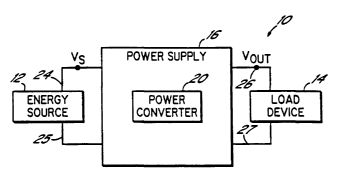
A typical arrangement is shown in FIG. 1 for a portable electronic device 10
that
includes an energy source 12, such as one or more batteries, and a load device
14, such as
the internal electronics that require electrical power. Interposed between the
energy
source 12 and he load device 14 is a power supply 16 that may perform a number
of
functions. For example, a power converter 20, depicted as integral to the
power supply
16, provides the necessary changes to the power from the energy source 12 to
make it
suitable for the load device 14.
The power supply 16 rnay also perform functions other than power conversion.
For example, protecting the energy source 12, load device 14 andlor power
converter 20
from damage by a sustained high electrical current may require electrically
disconnecting
the energy source 12 from the rest of the portable electronic device 10. As
another
example, the power converter 20 may require assistance during start-up which
is provided
by the supply 16.
With respect to the types of power conversion required, the power converter 20
may "step up" (i.e., boost) or "step down" the voltage. That is, the converter
20 may
increase or decrease the input voltage Vs from the energy source 12 across a
pair of input
terminals 24, 25 to an output voltage Tlo provided to the load device 14
across a pair of
output terminals 26, 27. The power converter 20 may also store an amount of
energy to
satisfy a brief spike or increase in demand by the load device 14 that the
energy source 12
is unable to provide.
The power converter 20 may also regulate the output voltage Tlo, keeping it
close
to the desired output voltage level and reducing rapid fluctuations that may
cause
detrimental noise or cause undesirable performance of the load device 14. Such
fluctuations may occur due to changes in demand by the load, induced noise
from
2
CA 02403725 2002-09-18
WO 01/71894 PCT/USO1/08454
external electromagnetic sources, characteristics of the energy source 12,
and/or noise
from other components in the power supply 16.
Inductive DC-DC power converters are often used in medium to medium/high
capacity switching power supplies. Known inductive DC-DC power converters are
based
upon switching an output stage between a charge and discharge state. The
output stage
includes a switch that, when closed during the charge state, causes an
inductive element,
such as an inductor to charge (i.e., to store energy in an electric field)
from the energy
source. A rectifying element, such as a diode, is non-conductive, thereby
preventing
discharging to a load capacitor across the output terminals. During the
discharge state,
the switch is opened and the rectifying element conducts allowing the inductor
to
discharge into the load capacitor.
Known inductive DC-DC power converters are configured in various ways in
order to achieve greater capacities, voltage ranges, and
inverting/noninverting outputs.
An inverted output has the opposite algebraic sign as the input. For example,
an input
voltage is provided at the positive input terminal 24 at +1.5 V referenced to
a grounded
negative input terminal 25. The positive output terminal 26 is grounded and
the negative
output terminal 27 is -1.0 V. Examples of known configurations include
converters
referred to buck, boost, buck-boost, noninverting buck-boost, bridge, Watkins-
Johnson,
current fed bridge, uk, single-ended primary inductance converter (SEPIC),
buck
square.
Inductive DC-DC power converters are often chosen due to power efftciencies
which are greater than other converters such as linear converters, whose
efficiency is
related to the ratio of output voltage Tlo to input voltage vs. Also, the
output voltage Yo
of inductive converters is generally related to the duty cycle of the
switching, rather than
the operating frequency of the switching, unlike generally known capacitive
power
converters.
However, known output stages for inductive DC-DC power converters 20 do have
some drawbacks related to the capacitor, switch, and rectifying elements used
in the
converter. Specif tally, reliance upon a diode as the rectifying element
imposes a voltage
drop across the diode that makes low input voltages (e.g., sub-one volt)
impractical. In
CA 02403725 2002-09-18
WO 01/71894 PCT/USO1/08454
addition, generally known switches similarly require a control signal of a
magnitude
unsuitable for low input voltages. In addition, the range of practical
inductance and
capacitance values is constrained by achievable operating frequencies of the
controller.
Therefore, relatively expensive, noisy, and relatively large discrete
inductors are required
~ for the power output stage within an inductive converter.
Furthermore, known inductive DC-DC power converters 20 rely upon oscillator-
based control. The inductor-capacitor combination chosen for these known
"oscillator-
controlled power converters" 20 generally dictate an operating frequency
suitable for
operation. Adjustments to the power delivered by the oscillator-controlled
power
converter is often provided by Pulse Width Modulation (PWM) or Pulse Frequency
Modulation (PFM) by a controller. The problems with PWM and PFM schemes
include
circuit and fabrication complexity. Such complexity results in difficulty in
miniaturizing
the power converter 20 due to the number of discrete components necessary
andlor the
required area allocated on a semiconductor device.
In addition to the drawbacks associated with their complexity, oscillator-
controlled power converters are also inefficient with light loads due to the
continued
operation of the oscillator.
Still further drawbacks in the prior art are the result of some inductive DC-
DC
power converters 20 using feedback, either inductor voltage VL or inductor
current iL,
feedback to sense the energy stored in the inductor as well as to sense the
output voltage
Yo. These feedback techniques cause problems due to the nature of PWM and PFM
control. For instance, inductor voltage VL feedback is an indirect approach to
sensing the
stored energy in the inductor L and introduces noise into the feedback voltage
VF, (which
is the same as or directly related to the inductor voltage VL,) due to
fluctuations in input
voltage Ys and/or demand by the load device 14. Using current feedback avoids
sources
of voltage noise; however, known current-feedback power converters 20 suffer
problems
with respect to inadequate robustness to noise disturbances in the current
feedback iF,
(which is the same as or directly related to the inductor current iL,)
resulting in premature
switching and reduced power converter stability.
4
CA 02403725 2002-09-18
WO 01/71894 PCT/USO1/08454
SUMMARY OF THE INVENTION
The invention overcomes the above-noted and other deficiencies of the prior
art
by providing an apparatus and method for a dynamically controlled inductive
DC/DC
power converter that efficiently transfers power from an energy source as
demanded by a
load device.
In particular, in one aspect consistent with the invention, a dynamic
controller
operates an inductive power output stage to transfer energy at a rate to
maintain an output
voltage Yo across a load capacitor CL. More particularly, a power converter
has a power
output stage that is operable to electrically couple to input terminals of an
energy source
input terminals and to output terminals of a load device. The power output
stage includes
an inductive element that is charged by an inductor current supplied by the
energy source
during a charge state. The power output stage also includes the load capacitor
that is
charged by the inductive element during a discharge state. The dynamic
controller is
responsive to input signals for selectively and non-oscillatorily generating
the control
signal S2 to open the switch in a discharge state and close the switch in the
charge state.
The input signals to the controller including one or more of an output voltage
across the
output terminals, an input voltage across the input terminals, a selectable
reference
voltage and a feedback voltage measured across the inductive element.
These and other objects and advantages of the present invention shall be made
apparent from the accompanying drawings and the description thereof.
BRIEF DESCRIPTION OF THE FIGURES
The accompanying drawings, which are incorporated in and constitute a part of
this specification, illustrate embodiments of the invention, and, together
with the general
description of the invention given above, and the detailed description of the
embodiments
given below, serve to explain the principles of the present invention.
FIGURE 1 is a top-level block diagram of a portable electronic device
incorporating a power supply with a power converter.
CA 02403725 2002-09-18
WO 01/71894 PCT/USO1/08454
FIGURE 2A is a top-level diagram of an output stage for a buck power
converter.
FIGURE 2B is a top-level diagram of an output stage for a boost power
converter.
FIGURE 3 is a top-level block diagram of a dynamically controlled inductive
power converter in accordance with the invention.
FIGURE 4 is one embodiment of a circuit for a start-stop controller for the
boost
power converter of FIG. 2B in accordance with the invention.
FIGURE 5 is an embodiment of a circuit for a voltage-feedback oscillator-less
controller for the boost power converter of FIG. 2B in accordance with the
invention.
FIGURE 6 is a flow diagram for the operation of the voltage-feedback
oscillator-
less controller of FIG. 5 in accordance with the invention.
FIGURE 7 is an embodiment of a start-up circuit for the boost power converter
of
FIG. 5 in accordance with the invention.
FIGURE 8 is a wave diagram for the start-up circuit of FIG. 7.
FIGURE 9 is a flow diagram for the operation of the start-up circuit of FIG.
7.
FIGURE 10 is an embodiment of a gain amplifier circuit for the boost power
converter of FIG. 5 in accordance with the invention.
FIGURE 11 is an embodiment of a voltage reference circuit for the boost power
converter of FIG. 5 in accordance with the invention.
FIGURE 12 is top-level block diagram of an embodiment of the comparator for
the boost power converter of FIG. 5 in accordance with the invention.
FIGURE I3 is an embodiment of a circuit for the comparator of FIG. 12 in
accordance with the invention.
FIGURE 14 is an embodiment of a circuit for the timing circuit of FIG. 5 in
accordance with the invention.
FIGURE 15 is an embodiment of a circuit for a current-feedback oscillatorless
controller for the boost power converter of FIG. 2B.
DETAILED DESCRIPTION OF INVENTION
An explanation of lalown inductive power converters will be helpful in
understanding the invention. Referring to FIG. 2A, a top-level diagram of a
known buck
6
CA 02403725 2002-09-18
WO 01/71894 PCT/USO1/08454
power output stage 30a for a power converter 31A is depicted, as an example of
a down
converter that provides an output voltage Yo that is less than the input
voltage Tls. The
buck output stage 30a is coupled to an energy source 12 at input terminals 24,
25 and to a
load device 14 at output terminals 26, 27 to deliver energy from the energy
source to the
load device. The energy source 12 provides an input voltage Ys and an input
current is.
The load device 14 receives a current io and an output voltage Tao.
The buck output stage 30a includes a switch MS, a rectifying element MR, an
inductive element, such as an inductor L, and a capacitance element, such as a
load
capacitor CL. The Ioad capacitor CL has its positive terminal 32 coupled to
the positive
output terminal 26 and its negative terminal 33 coupled the negative output
terminal 27,
which is also coupled to the negative input terminal 25 forming a ground
reference. The
load capacitor CL, thus, is charged to the output voltage ho. The inductor L
has its
positive end 34 coupled to a feedback voltage node VF. The feedback voltage VF
is
related to the voltage VL across the inductor L. The inductor L has its
negative end 35
coupled to the positive output terminal 26.
The rectifying element MR, implemented as a MOSFET configured as a
synchronous rectifier, has its positive terminal (source) 36 coupled to the
feedback
voltage node VF and its negative terminal (drain) 37 coupled the negative
input and
output terminals, 25, 27. The rectifying element MR closes in response to a
control
signal S 1 in order to act like a diode. The MOSFET of the rectifying element
MR has a
channel that conducts current in the reverse direction, and thereby acts like
a diode often
used in oscillator-controlled power converters 20, by having the source and
drain
reversed compared to the MOSFET switch MS. The switch MS has its positive end
(drain) 38 coupled to the positive input terminal 24 and its negative end
(source) 39
coupled to the feedback voltage node VF. The switch MS closes in response to
control
signal S2 turning ON.
During the discharge state, the control signal S1 is ON to close the
rectifying
element MR so that it conducts and the control signal S2 is OFF to open the
switch MS,
allowing the inductor L to discharge into the load capacitor CL. During the
charge state,
the control signal S 1 is OFF to open the rectifying element or make it non-
conductive MR
7
CA 02403725 2002-09-18
WO 01/71894 PCT/USO1/08454
and the control signal S2 is ON to close the switch MS, allowing the inductor
to be
energized by the input current is from the energy source 12.
Referring to FIG. 2B, a boost power output stage 30b for a power converter 31
illustrates a configuration suitable for increasing the output voltage ho with
respect to the
input voltage Ys. The boost power output stage 30b has its input terminals 24,
25, output
terminals 26, 27, and load capacitor CL configured as described above for the
buck power
output stage 30a. The inductor voltage vL is defined between the input
terminal 24 and
the feedback voltage node VF. This inductor voltage VL is thus equivalent to
the
feedback voltage TL minus the input voltage Vs.
Rectifying element MR has its negative end 37 coupled to VL? the feedback
voltage node VF and its positive end 36 coupled to the positive output
terminal 26.
Specifically, a MOSFET is configured as a synchronous rectifier with its drain
as the
negative end and its source as the positive end. MOSFET switch MS has its
positive end
(drain) coupled to the feedback voltage node YF and its negative end (source)
coupled to
ground. During the discharge state, the MOSFET switch MS opens in response to
control
signal S2 turning OFF and rectifying element MR closes in response to control
signal S 1
turning ON, coupling the energy source I2 and inductor L to the load capacitor
CL. Thus,
the input voltage VL and inductor voltage VL are added in order to boost the
output
voltage Yo imparted to the load capacitor CL. During the charge state, MOSFET
switch
MS closes in response to control signal S2 fuming ON, coupling the inductor L
across the
energy source 12. Rectifying element MR opens in response to control signal S
1 turning
OFF, disconnecting the load capacitor CL from the energy source 12 and
inductor L.
In accordance with one aspect of the present invention, the buck power output
stage 30a of FIG. 2A and the boost power output stage 30b of FIG. 2B are both
advantageously efficient and operable with a low input voltage (e.g., sub-one
volt) by
implementation as an integrated circuit fabricated in a 0.35 micron double
salicide
process (two metal, two poly salicide) utilizing MOSFET transistor switches
capable of
low threshold (e.g., sub-one volt) control, as described the following co-
pending and
commonly owned applications all filed on March 22, 2000: U.S. Serial No.
09/532,761,
entitled "Lateral Asymmetric Lightly Doped Drain MOSFET", naming Ying Xu et
al.
CA 02403725 2002-09-18
WO 01/71894 PCT/USO1/08454
(P&G Case No.7992), which is hereby incorporated by reference. In addition to
having a
low threshold control, the disclosed MOSFET devices have a low on-resistance,
directly
contributing to the efficiency of the power output stage 30a and 30b used in
accordance
with the invention.
Referring to FIG. 3, a power converter 41 is depicted in block diagram form,
illustrating oscillatorless, dynamic control of power transfer from an energy
source 12 to
a load device 14 coupled to the output voltage Yo across output terminals 26,
27 in
accordance with one aspect of the invention. The power converter 41 is
dynamically
controlled in that it adapts to the demands from the load device I4, even with
variations
IO in the input voltage Ys, and variation in the transfer and storage
characteristics of the
power converter 4I.
The power converter 41 is intrinsically voltage regulated in that the amount
of
energy transferred does not only correspond to the demand, but the rate of
energy transfer
is controlled so that the output voltage Yo remains within an accepted range.
This is
generally referred to as remaining within an acceptable voltage ripple VIP.
The power converter 41 includes a power output stage 42 that transfers the
stor ed
energy to the load device 14 and a power controller 46 coupled to the power
output stage
30 to responsively command the appropriate amount of stored energy to be
transferred in
accordance with the present invention.
In one embodiment, the power output stage 42 is an inductive DC-DC power
converter, of which the above described buck power output stage 30a and boost
power
output stage 30b are examples. The load capacitor CL is electrically coupled
across the
output terminals 26, 27. The load capacitor CL stores electrical charge and
provides the
output voltage yo in relation to its stored charge. The power output stage 42
also
incorporates the inductor L for transferring energy from the energy source 12
to the load
capacitor CL as discussed above. The series resistance for the inductor L and
the load
capacitor CL may advantageously be chosen to be low so that the power
converter 41 has
reduced power consumption. The power output stage 42 includes a switch matrix
48
coupled to the inductor L, load capacitor CL, and energy source 12 for
configuring the
power output stage 30 between a charge state and a discharge state.
9
CA 02403725 2002-09-18
WO 01/71894 PCT/USO1/08454
In addition, the power output stage 30 may be inverting or noninverting, with
respect to whether the output voltage has an opposite algebraic sign to the
input voltage
Ys. For example, a 2.2 V input voltage Ys may be converted to a -1.6 V output
voltage
Yo. Generally, noninverting embodiments are illustrated below for clarity,
although one
skilled in the art, having the benefit of the instant disclosure, should
recognize application
to inverting power converters.
Mufti-loop power controller 46 comprises a dynamic controller 50, a voltage
reference 52, and an environmental controller 64 to advantageously control the
power
output stage 42. The dynamic controller is responsive to feedback signals
which act as
input signals to the controller 50. A first control Ioop 56 is formed by the
output voltage
yo from output terminal 26 being provided as feedback to the dynamic
controller 50. The
dynamic controller 50 commands the switch matrix 48 to transfer additional
charge from
the energy source 12 to the load capacitor CL in response to the output
voltage Yo being
below a predetermined value VHF. The dynamic controller 50 makes the
determination of
whether Yo is below a predetermined value in comparison to a reference voltage
Tl~F
from voltage reference 52. One suitable VHF may be provided by the energy
source 12 if
it is sufficiently voltage stable to simplify the voltage reference 52 (e.g.,
lithium batteries
are voltage stable). Thus, the voltage reference 52 may then be provided by a
voltage
divider or multiplier of the input voltage Ys to achieve the desired reference
voltage VHF.
In addition to the first control loop 56, the mufti-loop power controller 46
is
responsive to a second control loop 58 or input signal. In the second control
loop 58, the
energy stored in the inductor L is sensed indirectly by the dynamic controller
50 as a
feedback voltage YF, which is the same as or directly related to the inductor
voltage UL.
Alternatively, the energy stored in the inductor L may be directly sensed as
the strength
of an electrical field created by inductor current iL, or by a feedback
current iF, which may
be the same as or directly related to the inductor current iL, as will be
discussed with
regard to FIG. 15 below. Thus, using the feedback signal associated with the
inductor,
any discharge of the inductor L upon demand may be predicated upon the
inductor L first
reaching an optimum state of charge (i.e., energy stored in the form of an
electrical field).
CA 02403725 2002-09-18
WO 01/71894 PCT/USO1/08454
The optimum state of charge exists because undercharging the inductor L
results in
unnecessary switching power losses and overcharging the inductor L
unnecessarily limits
the rate of power transfer.
Regarding unnecessary switch power losses, dynamic control of the switch
matrix
S 48 achieves efficiency in part as described with the first control loop by
remaining in the
discharge state until more charge is needed (i.e., until ho drops below T~~F).
Prior art
oscillator-controlled power converters 20, by contrast, are switched at a
fixed rate even
when not necessary. Therefore, the present invention is oscillatorless and
provides
control non-oscillatorily even though it will switch periodically, because the
switching is
determined by feedback control and does not continuously oscillate at a fixed
frequency.
Additional efficiency in the dynamic control of the switch matrix 48 is
realized by
remaining in the charge state long enough fox the inductor L to acquire a
significant
amount of charge. For example, charging to 40% rather than 80% of full charge
would
require that the operating frequency would double to transfer the same power.
The switch
1 S MS and rectifying element MR dissipate power in relation to this increased
operating
frequency. This is due to low-on resistance and high-off resistance of the
Field Effect
Transistors used. Since power consumption is a function of the square of the
current
times the resistance, most of the power loss occurs during the transition.
Consequently,
the second control Loop S8 senses the voltage Ievel across the inductor L to
avoid
undercharging during the charge state, and thus avoid unnecessary switching
losses.
Optimizing the charge on the inductor L in accordance with one aspect of the
invention also includes avoiding overcharging. Inductors are characterized by
their rate
of charging as a function of time. Specifically, as inductors approach a fully
energized
condition, their rate for accepting additional energy decreases. Thus, the
initial amount of
2S energy acquired by the inductor takes less time than a later similar amount
of energy. For
example, it would take Less time to energize the inductor L twice to 4S% than
to energize
the inductor L once to 90%, even though the same amount of energy would be
accepted
by the inductor L. Consequently, leaving the switch matrix 48 in the charge
state for a
period of time longer than required to achieve the optimum level of charge of
the inductor
L misses an opportunity to transfer more power.
11
CA 02403725 2002-09-18
WO 01/71894 PCT/USO1/08454
It should be appreciated that the optimum level of stored energy for a
particular
inductive component may be determined empirically and/or analytically as would
be
apparent to those skilled in the art having the benefit of the instant
disclosure.
In combination with one or more other control loops 56, 58 discussed above,
the
power converter 41 may advantageously include a forward control loop 60 as an
input
signal whereby one or more parameters of the energy source 12 are provided to
the
dynamic controller 50. One use of the forward control Ioop 60 would include
disabling
(i.e., interrupting output current to the output terminals 26, 27) and/or
bypassing (i.e.,
directly coupling the energy source 12 to the output terminals 26, 27) the
power converter
31 due to unsafe conditions or performance limiting conditions sensed in the
energy
source 12. For example, a low input voltage may indicate inadequate remaining
charge in
the energy source 12 to warrant continued operation of the power converter 31.
As
another example, the electrical current drawn from the energy source 12 may be
too high
for sustained operation. Thus, a protection circuit may be included in the
power converter
41 for interrupting output current to the output terminals 26, 27 based upon
control loop
60.
As yet an additional example of dynamic control, a large demand by the load
device 14 may warrant continued operation of the power converter 41 in
parallel to a
direct coupling of the energy source 12 to the output terminals 26, 27. This
may be
especially true when the input voltage Vs and desired output voltage Tlo are
approximately the same. An increased output current capacity is achievable by
having
two paths providing current to output terminals 26, 27.
As a further example, the feedback voltage YF (second control loop 58), and
the
input voltage Vs (forward control loop 60) may indicate that the power
converter 41 is
fully discharged and is in a start-up condition. This start-up condition may
advantageously warrant use of a rapid progressive start-up circuit, an example
being
described below in accordance with one aspect of the invention.
In combination with one of the other control loops or control input signals
56, 58,
and 60, the power controller 46 may further include an adaptive control loop
62, as
represented by an environmental controller 64. The environmental controller 64
senses a
12
CA 02403725 2002-09-18
WO 01/71894 PCT/USO1/08454
control parameter 66 and provides a command 68 to the dynamic controller 50
for
altering the predetermined value for the output voltage Yo. For example, the
environmental controller 64 may sense that the dynamic controller 50 has
become
unstable, and in response thereto, may provide a signal to drive the dynamic
controller 50
to a stable output condition. More particularly, the environmental controller
64 may be
adapted to sense an unstable operating condition of the power converter 41,
such as the
instantaneous output voltage and current each approaching a constant value.
The
environmental controller 64 may then adjust the predetermined value to drive
the power
converter 41 to a stable operating condition. Moreover, such altering of the
predetermined value may include resetting of the dynamic controller 50 to a
stable initial
condition.
As another example, the adaptive control loop 62 may include a control signal
S~
that is input to the environmental controller 64 whereby the dynamic
controller 50 can be
made to respond to changes in a load device 14 (e.g., CPU, volatile memory,
analog-to-
digital converter, digital-to-analog converter) or to other parameters. The
load device 14
may advantageously perform better with an adjusted output voltage Yo from the
power
converter 41. As another example, the output control signal S~ may be a
reconfiguration
control signal, such as for selecting a desired inverting or noninverting mode
or
predetermined output voltage Yo. As yet another example, a protective function
(e.g.,
bypassing, disabling, or altering the output voltages) may be dictated by the
S~ command
to preclude damaging a load device 14. For example, the load device 14 may
fail under
high current, and thus, limits may be imposed to preclude this occurrence.
Depending upon the type of switch matrix 48 that is utilized in the invention,
various control signals are generated by the dynamic controller 50 for the
switch matrix
48, as represented by switch signals S1, S2, S3 to SN. For example, control
signals S3 to
SN may represent inputs for a configuring the power output stage 42 to various
combination in order to provide a step up, step down, inverted, and/or
noninverted output
arrangement.
13
CA 02403725 2002-09-18
WO 01/71894 PCT/USO1/08454
It should be appreciated that the inductor L and the load capacitor CL are
illustrative of charge storage and transfer components and may represent
discrete
elements or integrated circuit elements.
Moreover, due to the flexibility of the dynamic controller 50, the load
capacitor
CL may include various levels of storage capability, such as with small
capacitors (e.g.,
ceramic, chip thick film, tantalum, polymer) and large capacitors (e.g., ultra-
capacitors,
pseudo-capacitors, double-layer capacitors). The amount of inductance and
capacitance
is reflective of the amount of storage capability. Thus, providing the same
amount of
energy transfer requires either that small doses of energy be transferred from
a small
inductor L with a high operating frequency or that larger doses of charge be
transferred
more slowly. Thus, the power converter 41 is flexible in that the same dynamic
controller
50 may control various power output stages 42. In particular, unlike the prior
art
oscillator-controlled power converter 20, the dynamic controller 50 may
operate in the
low operating frequency range appropriate for power output stages 30
incorporating ultra-
capacitors.
It should further be appreciated that the energy source 12 may include various
electrical charge storage or generating devices such as one or more
electrochemical cells
(e.g., a battery), photovoltaic cells, a direct-current (DC) generator (e.g.,
a wrist watch
charged by a motion- powered generator in combination with a rechargeable
battery), and
other applicable power sources.
As another example, power converters 41 consistent with the invention may be
used advantageously in electronic devices powered by other power supplies. For
example, a device receiving its power from a standard alternating current (AC)
wall plug
generally transforms the AC power into direct current (DC) power for
electronic portions
of the device. The DC power provided may be unsuitable for all or portions of
the
electronics without further adjustment and regulation. For example, a
microprocessor
may be operating at 2.2 V whereas input/output electronics may operate at 5 V.
Consequently, a power converter 41 in accordance with the invention may be
used to
step-down the input voltage to the microprocessor.
14
CA 02403725 2002-09-18
WO 01/71894 PCT/USO1/08454
Referring to FIG. 4, one embodiment of a circuit for a start-stop controller
SOa for
the power output stage 30b of FIG. 2B is illustrated. Generally known power
converters
20, including inductive power converters, continue to oscillate, even when the
demand
from the load device 14 makes the power converter inefficient. Consequently,
the start-
s stop controller advantageously stops the oscillation of a Pulse Width
Modulation (PWM)
output when the load capacitor CL is adequately charged.
Specifically, the boost power output stage 30b is as described above in FIG.
2B,
except for the addition of a capacitive element C1 coupled across input
terminals 24, 25
which is used to enhance the stability of input voltage Ys.
I0 The start-stop controller SOa is responsive to input signals for pulse
width
modulation (PWM), and oscillated control of the power output stage 30b by
selectively
generating the control signal S 1 to close the rectifying element MR during
the discharge
state and to open the rectifying element MR during the charge state, and
selectively
generating the control signal S2 to open the switch MS during the discharge
state and to
15 close the switch MS during the charge state. The staut-stop controller SOa
senses a low
demand as indicated by the comparison of the reference voltage VHF and the
output
voltage Vo to hysteretically stop the oscillated control signal so that the
output stage 30b
remains in the discharge state. The start-stop controller SOa includes a
hysteretic
comparator 70 responsive to the reference voltage V~,F, the output voltage Vo
and the
20 feedback voltage VF to generate a duty-cycle signal, and hysteretically
responsive to the
output voltage vo and the reference voltage Y~F to generate a stop signal. A
modulator
72 generates an oscillation signal having the predetermined frequency. An SR
flip flop
74 is set by the set duty-cycle signal and reset by the oscillation signal to
produce a
switching signal which determines the charge state and the discharge state. A
multiplexer
25 75 is responsive to the switching sigmal to generate the control signals S
1 and S2. The
multiplexer 75 has a predetermined state switching delay to mitigate cross
conduction of
the power output stage 30b. The multiplexer 75 is also responsive to the stop
signal to
stop oscillations until more energy is needed by turning OFF control signal S2
to open
switch MS and by turning ON control signal S1 to close rectifying element MR.
CA 02403725 2002-09-18
WO 01/71894 PCT/USO1/08454
In addition, a start-up circuit 76 biases the start-stop controller SOa when
the
power output stage 30b is discharged, as well as providing initial charge to
the load
capacitor CL.
Referring to FIG. 5, an embodiment of a circuit for a voltage-feedback dynamic
controller SOb is shown as used for a boost power converter such as shown in
FIG. 2B. In
particular, the first control loop 56 provides the output voltage Vo and the
second control
loop 58 provides the feedback voltage VF to the dynamic controller SOb, which
provides
control of the chargeldischarge states of the converter with control signals
S1 and S2.
The start-up circuit 76 is powered by the input voltage Vs from the input
terminal
I O 24. The start-up circuit 76 responds to the feedback voltage VF such that
when the power
output stage 30b is fully discharged and thus the controller SOb is not yet
operating, the
start-up circuit 76 provides a bias to the voltage reference 52, to a gain
amplifier 78 and
to the dynamic controller SOb.
The gain amplifier 78 receives the output voltage Tlo and the feedback voltage
VF
respectively from the first and second control loops 56, 58, and provides a
desired bias
and gain to each to produce a filtered and amplified output voltage V'o and
feedback
voltage VF. The desired bias and gain may be selected for appropriate
responsiveness
and stability of the dynamic controller SOb.
The dynamic controller SOb receives as input signals the input voltage Vs, the
reference voltage VHF from the voltage reference 52, the filtered feedback
voltage VF,
and the filtered output voltage Yo. More particularly, during the discharge
state, the
dynamic controller SOb couples the reference voltage TT~F to a positive
comparator input
80 via a switch M2 responsive to a control signal S1'. The dynamic controller
SOb
couples the filtered output voltage Vo to a negative comparator input 81 via a
switch M4
responsive to the control signal Sl'. During the charge state, the dynamic
controller SOb
couples the input voltage input voltage vs to the positive comparator input 80
via a switch
M1 responsive to a control signal S2'. The dynamic controller SOb further
couples the
filtered feedback voltage VF to the negative comparator input 81 via a switch
M3
responsive to the control signal S2'.
16
CA 02403725 2002-09-18
WO 01/71894 PCT/USO1/08454
The dynamic controller includes a comparator 82 for generating a comparison
signal based on the input to the positive and negative comparator inputs 80,
81, as
described in FIG. 6 below. The comparison signal is used by a timing circuit
84 to
produce the control signals S1, S2, Sl', S2', S1N and S2N, as described below
in FIG. 14.
Control signal S 1 is used to control the rectifying element MR, and has
sufficient current
to control a power MOSFET. Control signal S2 is used to control the switch MS,
and has
sufficient current to control a power MOSFET. S 1' and S2' are unamplified
versions of
control signals S1, S2, used within the dynamic controller SOb. Control
signals S1N and
S2N are inverted versions respectively of control signals Sl, S2, used for
controlling the
start-up circuit 76.
Referring to FIG. 6, a flow diagram for an operation 100 of the voltage-
feedback
dynamic controller SOb of FIG. S is shown. The operation 100 begins with the
controller
not operating, and thus control signals S 1 and S2 are OFF (block 102). Thus a
start-up
operation 104 is performed, as described below in more detail with respect to
FIGS. 7-9.
Then operation 100 begins dynamic operation, alternating as required between
charge and
discharge states.
Then, a determination is made as to whether the output voltage Yo is less than
the
reference voltage Y~F (block 106). If not, then the load capacitor CL is
sufficiently
charged and operation 100 repeats block 106, remaining in the discharge state.
However, if in block 106 the output voltage Yo is less than the reference
voltage
Y~F, then a start-up delay is performed (block 108). Then, control signal S 1
is turned
OFF, opening rectifying element MR (bloclc 110). A cross conduction delay
occurs
thereafter with control signal S2 already OFF and switch MS is open (block
112). This
prevents inefficient shorting of the power output stage 30b. Then, control
signal S2 is
2S turned ON, closing the switch MS, beginning the charge state (block 114).
At block 116, a determination is made as to whether the inductor L is
sufficiently
energized by determining whether the feedback voltage TlF is greater than or
equal to a
predetermined fraction ~i of the input voltage Vs, where 0 < ~i< 1, with block
116
repeating until satisfied.
17
CA 02403725 2002-09-18
WO 01/71894 PCT/USO1/08454
The fraction (3 is chosen either analytically or empirically for providing an
optimum energy transfer amount. A relatively small fraction [3 results in a
higher
operating frequency of switching. Since typical switches dissipate energy
mostly during
the transition from OFF to ON and from ON to OFF, minimizing switching
increases
efficiency. However, a relatively high fraction (3 limits the capacity of the
power output
stage 30b since the inductor L has a diminishing rate of energy storage as it
approaches a
fully energized state.
When block 116 is satisfied, then a start-up delay is performed (block 118).
Then,
the control signal S2 is turned OFF, opening the switch MS (block 120). A
cross
conduction delay occurs thereafter with control signal S2 already OFF and
switch MS
now open (block 122). Then control signal S 1 is turned ON, closing the
rectifying
element MR, beginning the discharge state. Operation 100, thus returns to
block 106 to
repeat the sequence.
FIG. 7 is an embodiment of a start-up circuit 76 for the boost power converter
of
FIG. 5.
FIGURE 8 is a wave diagram for the start-up circuit 76 of FIG. 7.
Referring to FIG. 9, the operation 104 of the start-up circuit 76 of FIG. 7 is
illustrated. The start-up operation 104 begins with an initial condition in
block 150 that a
load is already applied to the power converter and in block 152 that an input
voltage is
available to the power converter. Then a determination is made as to whether
the power
controller is off and not controlling the power output stage (block 154). If
the power
controller is on (block 154), then a small start-up capacitor CQp~p 1S floated
(block 156)
and the start-up operation 104 is complete.
Tt should be appreciated that the controller SOb is off with respect to the
start-up
operation 104 even after the controller begins to operate. That is, control
signals to the
start-up circuit 76 generally becomes available before the controller actually
has
developed a sufficient voltage to operate the rectifying element MR and the
switch MS.
If in block 154 the controller is off, then a start-up switch is closed to
provide
input voltage Ys to the start-up capacitor CQp~p (block 158) and the start-up
capacitor
CQPUMP is referenced to ground (block 160). When the start-up capacitor CQP~
is
18
CA 02403725 2002-09-18
WO 01/71894 PCT/USO1/08454
charged (block 162), it is first used to bias the controller (block 164), and
then discharged
into the load capacitor (block 166) and the start-up circuit including start-
up capacitor
CQPUMP is uncoupled from the power output stage of the power converter (block
168).
Then, the start-up operation 104 returns to block 154 to see if this start-up
cycle was
sufficient to activate the controller and subsequent start-up operation cycles
repeated as
necessary.
Referring to FIG. 10, an embodiment of the gain amplifier circuit 78 for the
dynamic controller SOb of FIG. S is depicted. The gain amplifier circuit 78
accepts as
input signals the feedback voltage Y~ and the output voltage Yo. An
operational amplifier
180 is biased by the start-up circuit 76. The positive input of the
operational amplifier
180 is the input which is coupled through voltage divider R3/R4. The negative
input and
output of the operational amplifier are coupled for feedback through resistors
RI and R2.
The resistors may be integrated (e.g., poly resistors) and of high impedance
(e.g., mega-
ohm range) for low power consumption.
Referring to FIG. 1 I, one embodiment of a voltage reference circuit 52 is
shown
for the boost power converter 30b of FIG. 5, capable of sub-one volt input
voltage 1s
operation in accordance with an aspect of the invention. A constant current
circuit 200
powers a voltage reference-to-rail circuit 202, isolating the voltage
reference-to-rail
circuit 202 from changes in the input voltage Ys. An output buffer 204
amplifies an
unamplified reference voltage from the voltage reference-to-rail circuit 202.
In order to
temperature compensate the voltage reference-to-rail circuit 202, a parallel
diode array
Proportional to the Absolute Temperature (PTAT) circuit 206 biases the circuit
202.
Referring to FIGS. 12 and 13, one embodiment of a comparator 82 is depicted
for
the boost power converter 30b of FIG. 5. Differential amplifiers 206-210 are
advantageously used since they are effective in rejecting common-mode signals.
For
example, common-mode signals may be induced noise on the inputs. Integrated
circuit
differential amplifiers have relatively low output gain. This has implications
in two
ways: non-linearity in an input transistor and in providing necessary current
gain fox the
timing circuit 84.
19
CA 02403725 2002-09-18
WO 01/71894 PCT/USO1/08454
For providing some cancellation of input non-linearity, a three differential
amplifier combination is depicted, wherein the first differential amplifier
206 receives a
V+ input at its negative input and V- at its positive input. A second
differential amplifier
208 receives V-. at its negative terminal and V+ at its positive terminal. The
output of the
first differential amplifier 206 is coupled to a negative terminal of a third
differential
amplifier 210 and the output of the second differential amplifier 208 is
coupled to a
positive input of the third differential amplifier 210. A fourth differential
amplifier 212 is
configured as a voltage follower buffer to increase the current of a
comparator switching
signal (Out+, Out-) from the third differential amplifier 210.
Referring to FIG. 14, one embodiment of the timing circuit 84 is depicted for
the
power controller 46A of FIG. 5.
Referring to FIG. 15, an embodiment of a circuit for a current-feedback
oscillator-
less dynamic controller SOb is shown for the boost power output stage 30b of
FIG. 2B.
Specifically, a feedback current iF sensed by a current probe 300 at feedback
voltage TlF
node. The feedback current iF is related to, or the same as, the inductor
current iL. The
sensed feedback current iF is converted into a feedback voltage VF by a
current converter
302 for an input to the gain amplifier 78 as described above.
While the present invention has been illustrated by description of several
embodiments and while the illustrative embodixnents have been described in
considerable
detail, it is not the intention of applicants to restrict or in any way limit
the scope of the
appended claims to such detail. Additional advantages and modifications
readily appear
to those skilled in the art.
For example, for clarity, the switch MS and rectifying element MR are normally
open, closed by a positive ON signal. It would be apparent to those skilled in
the art
having the benefit of the instant disclosure to use normally closed switches
and/or
switches closed by a negative ON signal.
As another example, a power converter consistent with the invention may be
incorporated in a wide range of products. For example, a power converter 31
taking
advantage of the small size and low power consumption (i.e., efficiency)
properties
described above may advantageously be incorporated into a battery package to
enhance
CA 02403725 2002-09-18
WO 01/71894 PCT/USO1/08454
battery service life and energy and amplitude on demand. Incorporating the
power
converter would be accomplished in manner similar to that disclosed in the
following co-
pending and commonly owned applications all filed on April 2, 1998: U.S.
Serial No.
09/054,192, entitled PRIMARY BATTERY HAVING A BUILT-IN CONTROLLER TO
EXTEND BATTERY RUN TIME, naming Vladimir Gartstein and Dragan D. Nebrigic; .
U.S. Serial No. 09/054,191, entitled BATTERY HAVING A BUILT-IN CONTROLLER
TO EXTEND BATTERY SERVICE RUN TIME naming Vladimir Gartstein and Dragan
D. Nebrigic; U.S. Serial No. 091054,087, ENTITLED BATTERY HAVING A BUILT-IN
CONTROLLER, naming Vladimir Gartstein and Dragan D. Nebrigic; and U. S.
Provisional Application Serial No. 60/080,427, entitled BATTERY HAVING A BUILT-
IN CONTROLLER TO EXTEND BATTERY SERVICE RUN TIME, naming Dragan D.
Nebrigic and Vladimir Gartstein. All of the aforementioned applications are
hereby
incorporated by reference in their entirety.
21