Note: Descriptions are shown in the official language in which they were submitted.
CA 02404059 2003-09-09
-1 -
TITLE OF THE INVENTION
METHOD AND APPARATUS FOR PROVIDING OPTIMIZED ACCESS TO
CIRCUITS FOR DEBUG, PROGRAMMING, AND TEST
STATEMENT REGARDING FEDERALLY SPONSORED RESEARCH OR
DEVELOPMENT
NIA
BACKGROUND OF THE INVENTION
The present invention relates to apparatus and methods for accessing
electrical nodes of electronic circuits for programming, testing, or debugging
purposes.
One way of providing access to electrical nodes of
Integrated Circuits (ICs) is commonly referred to as "scan testing," which
typically involves serially shifting digital data into state elements included
in an IC to apply logic levels to selected nodes as test stimuli, and serially
shifting digital date out of the state elements to capture logic levels
generated
at other nodes in response to the test stimuli. Such control and observation
of an IC's electrical nodes via state elements is also used to provide
"visibility"
into an IC for debugging purposes. Further, an IC that supports scan
CA 02404059 2002-09-20
WO 01/71876 PCT/USO1/08884
-2-
testing is frequently used to access electrical nodes of
other electronic circuits connected thereto. For example,
these other electronic circuits may be embedded within the
IC, i.e., embedded memories or cores, or .externally
connected to the IC.
Scan testing is typically performed in accordance
with the IEEE 1149.1 Standard described in the IEEE
1149.1-1990 Standard Test Access Port and Boundary Scan
Architecture specification. The IEEE 1149.1 Standard was
primarily developed to solve problems related to Printed
Circuit Board (PCB) testing. The IEEE 1149.1 Standard is
also typically used to access "scan chains" within ICs to
facilitate testing and debugging of ICs, PCBs, and
systems.
"Boundary scan" is an application of scan testing at
input and output (I/0) pins of an IC to provide direct
control and observation of electrical nodes using boundary
scan operations. Boundary scan involves a specific type
of scan path having a boundary scan register cell at each
I/O pin of an IC. For example, by performing boundary
scan operations, known logic levels may be placed directly
on outputs of one circuit and observed at inputs of
another circuit connected thereto. Boundary scan
therefore provides a way of determining whether circuits
are properly connected to each other on, e.g., a PCB,
and/or whether there are manufacturing defects on the PCB
that may prevent the circuits from carrying out their
intended mission. Boundary scan tests can detect
different types of defects on a PCB, e.g., broken circuit
traces, cold solder joints, solder bridges, and
CA 02404059 2002-09-20
WO 01/71876 PCT/USO1/08884
-3-
electrostatic-discharge (ESD) induced failures in IC
buffers .
Fig. 1 depicts boundary scan architecture 100, which
is compliant with the IEEE 1149.1 Standard a.nd may be
embedded in an IC to provide direct control and
observation of electrical nodes via the IC's I/O pins. As
depicted in Fig. 1, an IC compliant with the IEEE 1149.1
Standard includes the following four (4) mandatory pins:
TDI, TDO, TCK, and TMS. Further, the IC optionally
includes the pin, TRSTN. These pins, TDI, TDO, TCK, TMS,
and optionally TRSTN, are commonly known as the Test
Access Port (TAP).
In addition, the IC includes three (3) mandatory scan
registers, i.e., an Instruction Register (IR) 104; and,
two (2) Data Registers (DRs), i.e., a Boundary Scan
Register (BSR) 106 and a Bypass Register (BYPASS) 108.
Further, the IC optionally includes at least one User DR,
i.e., a User DR 110, which may be used to implement tests
such as internal scan path testing and Built-In Self-Test
(BIST). Moreover, the IC includes a protocol interface
102 known as a TAP Controller, which includes a 16-state
Finite State Machine (FSM) operated by the mandatory TMS
and TCK input pins and other logic.
Fig. 3 depicts a state diagram 300 for the standard
FSM of the Tap Controller 102. A logic level on the TMS
pin determines a next state of the FSM, and a clock signal
on the TCK pin causes state transitions to occur.
Further, an updated IR instruction selects the IR 104, the
BSR 106, the BYPASS DR 108, or the USER DR 110 for scan
operations. Moreover, the FSM includes a Select-DR branch
301 that defines states for performing a "DR-scan"
CA 02404059 2002-09-20
WO 01/71876 PCT/USO1/08884
-4-
operation and a Select-IR branch 303 that defines states
for performing an "IR-scan" operation.
The IR 104, the BSR DR 106, the BYPASS DR 108, and
the USER DR 110 each comprise a separate scan .path; and,
the TAP Controller 102 enables operation of only one of
these scan registers at a time. The selected scan
register shifts its scan data between the TDI pin and the
TDO pin during a Shift-IR 324 state or a Shift-DR 310
state. Further, the selected scan register for the next
set of scan operations is determined by the IR instruction
that was previously updated in the IR 104 during an
Update-IR 332 state. Moreover, the IEEE 1149.1 Standard
uses both edges of the clock signal on the TCK pin.
Specifically, a logic level on the TMS pin and scan data
on the TDI pin are sampled on the rising edge of the clock
signal, and scan data on the TDO pin changes on the
falling edge of the clock signal.
The state diagram 300 of Fig. 3 includes six (6)
~~steady-states," i.e., a Test-Logic-Reset 302 state, a
Run-Test/Idle 304 state, a Shift-DR 310 state, a Pause-DR
314 state, a Shift-IR 324 state, and a Pause-IR 328 state.
According to the IEEE 1149.1 Standard, there is only one
(1) steady-state when the TMS pin is set to logical 1,
i.e., the Test-Logic-Reset 302 state; and, the FSM of the
TAP Controller 102 can be reset (i.e., transition to the
Test-Logic-Reset 302 state) within five (5) TCK clock
signal transitions while the TMS pin is set to logical 1.
The optional TRSTN pin provides another way to reset the
FSM of the TAP Controller 102. For example, setting the
TRSTN pin to logical 0 causes an asynchronous reset of the
TAP Controller 102 FSM.
CA 02404059 2002-09-20
WO 01/71876 PCT/USO1/08884
-5-
The DR branch 301 and the IR branch 303 of the TAP
Controller 102 FSM each includes six (6) states.
Specifically, a Capture state, e.g., a Capture-DR 308
state and a Capture-IR 322 state, causes a selected scan
register to capture data via parallel inputs of the scan
register. This captured data is shifted out of the
selected register on the TDO pin during the Shift-DR 310
state or the Shift-IR 324 state, while new scan data is
simultaneously shifted into the register via the TDI pin.
After the scan shift operation is completed, new scan
data is updated into a parallel update stage of the scan
register. An IR or DR update operation is enabled upon
entering either the Update-IR 332 state or the Update-DR
state 318, respectively.
A state sequence including an Exit1-DR 312 state,
immediately followed by a Pause-DR 314 state, and
immediately followed by an Exit2-DR 316 state is used to
terminate or suspend the Shift-DR 310 state operation.
Similarly, a state sequence including an Exitl-IR 326
state, immediately followed by a Pause-IR 328 state, and
immediately followed by an Exit2-IR 330 state is used to
terminate or suspend the Shift-IR 324 state operation.
The Pause-DR 314 state and the Pause-IR 328 state are
included in the TAP Controller 102 FSM primarily to
account for potentially slow tester hardware and/or
software performance.
The instructions updated in the IR 104 not only
select scan registers for shifting scan data, but also
determine test behavior, e.g., for boundary scan testing
of PCB interconnects. The IEEE 1149.1 Standard specifies
three (3) mandatory instructions and their corresponding
CA 02404059 2002-09-20
WO 01/71876 PCT/USO1/08884
-6-
test behavior. One such instruction is the BYPASS
instruction, which selects the BYPASS DR 108 to provide a
1-bit scan path between TDI and TDO. For example, scan
paths of multiple circuits compliant with the hEEE 1149.1
Standard may be chained together by serially connecting
their respective TDI and TDO pins. The BYPASS instruction
may then be used to "bypass" these potentially long scan
paths when DRs corresponding thereto do not have to be
accessed for particular test or debug operations. In this
way, the BYPASS instructions) may be used to reduce the
number of scan bits that are shifted.
Other mandatory instructions are the SAMPLE/PRELOAD
and EXTEST instructions, both of which select the BSR 106.
Specifically, the SAMPLE/PRELOAD instruction is used to
sample logic levels on an IC's I/O pins during normal
operation and pre-load data into the BSR 106 before
testing. The IC's I/0 pins are controlled by normal
system logic during the SAMPLE/PRELOAD instruction. The
EXTEST instruction controls the IC's I/O pins from the BSR
106 and may be used to perform PCB interconnect testing.
Although the boundary scan architecture 100 can be
used to program, test, and debug electronic circuits, the
boundary scan architecture 100 has several drawbacks. For
example, in accordance with the IEEE 1149.1 Standard, the
Pause-IR 328 state and the Pause-DR 314 state are included
in the Select-IR branch 303 and the Select-DR branch 301,
respectively, of the TAP Controller 102 FSM primarily to
account for less than optimal tester hardware and/or
software performance. However, the hardware and software
of today's test resources are normally fast enough to
shift scan data continuously without requiring the Pause-
CA 02404059 2002-09-20
WO 01/71876 PCT/USO1/08884
IR 328 and Pause-DR 314 states. Accordingly, these states
merely increase the time required to perform such shift
operations.
In addition, in ICs compliant with the LEEE 1149.1
Standard and PCBs including such components, it is
frequently difficult to access electrical nodes of non
scan sequential circuits from scan paths surrounding these
circuits. Such non-scan sequential circuits may include
non-scan embedded cores and component clusters on PCBs.
The IEEE 1149.1 Standard is particularly inefficient when
used to access memories, whether the memories are embedded
within an IC or externally connected to an IC. This is
because memories typically require long and/or complex
control and address sequences to fully access their
contents and provide comprehensive testing thereof, and
ICs compliant with the IEEE 1149.1 Standard often cannot
efficiently handle such long and complex sequences.
Specifically, if the BSR 106 of an IC were used to
move data to a memory externally connected to the IC, then
read/write cycles of the memory would typically be
emulated using the Select-DR branch 301 of the TAP
Controller 102 FSM, and data would typically be shifted
into the BSR 106 to sequence the data, address, and
control signals of the memory. This is conventionally
done by putting the IC into the EXTEST mode, shifting a
pattern of address, data, and control values into
corresponding bit positions of the BSR 106, and updating
the BSR 106 to apply the bit pattern to the memory in
parallel.
However, any change in a control value, e.g., to
place a logical 0 on a write enable (WEN) pin, therefore
CA 02404059 2002-09-20
WO 01/71876 PCT/USO1/08884
_g_
requires multiple BSR shift operations. This can be very
inefficient for complex access sequences, wherein several
BSR scan operations may be required to read from or write
to a single address location of the memory. Further,
read/write control sequences must be serialized to apply
these same sequences through the BSR 106.
Still further, each BSR scan operation scans all of
the bits in the BSR 106, not just those bits needed to
access the memory data, address, and control signals.
This also decreases efficiency because in a typical IC
with high-density I/0 packaging, e.g., a Ball Grid Array
(BGA), the BSR 106 can be several hundred bits in length
yet only a fraction of these bits typically needs to be
accessed to control the memory signals.
In addition, the protocol of the TAP Controller 102
FSM prohibits certain types of testing. Specifically, the
TAP Controller 102 FSM does not provide for a state
sequence including the Shift-DR state, immediately
followed by the Capture-DR state, and immediately followed
by the Shift-DR state, which is normally required for
controlling internal scan registers; or, a state sequence
including the Update-DR state immediately followed by the
Capture-DR state, which is normally required for
performing path delay testing of interconnects.
It would therefore be desirable to have improved
apparatus and methods that provide for the access of
electrical nodes of electronic circuits including scan and
non-scan sequential circuits and combinatorial circuits.
It would also be desirable to have improved apparatus and
methods that efficiently access electrical nodes of
CA 02404059 2002-09-20
WO 01/71876 PCT/USO1/08884
-9-
electronic circuits that require long and/or complex
control and address sequences.
BRIEF SUMMARY OF THE INVENTION
In accordance with the present invention, apparatus and
methods are disclosed for providing optimized access to
electrical nodes of electronic circuits for programming,
testing, and debugging. The presently disclosed apparatus
includes an access interface circuit that can be connected
between a test resource and an electronic circuit such as a
circuit adapted for scan testing, a non-scan sequential
circuit, a component cluster, or a memory circuit. The
access interface circuit includes a protocol generator,
which has a control register queue and an address register;
and, a data generator, which has a plurality of registers
adapted for capturing, shifting, and/or updating data
samples. Address and control sequences for
programming/testing/debugging the electronic circuit can be
serially loaded into the control register queue and the
address register using the test resource. Data sequences
for programming/testing/debugging the electronic circuit can
also be serially loaded into the data registers using the
test resource. The access interface circuit also includes
circuitry for switchably and directly applying either the
serially loaded address and control sequences or the normal
system address and control signals to the electronic
circuit; and, for switchably and directly applying either
the serially loaded data sequences or the normal system data
signals to the electronic circuit. The access interface
circuit further includes circuitry for directly capturing
data values from the electronic circuit in the data
CA 02404059 2002-09-20
WO 01/71876 PCT/USO1/08884
-10-
registers. The access interface circuit therefore allows
complex access sequences to be efficiently applied to the
electronic circuit, and data sequences to be efficiently
written to and read from the electronic circuit under
control of the test resource. Such capability is
particularly useful in programming/testing/debugging memory
and non-scan circuits.
The presently disclosed apparatus further includes a
programmable controller connected to the access interface
circuit and connectable to the test resource. The
programmable controller includes a state machine having a
plurality of states at least one of which is programmable.
The access interface circuit performs operational commands
based on at least a portion of the plurality of states.
Because the state machine is programmable, the programmable
controller enhances the flexibility of the access interface
circuit for programming/testing/debugging electronic
circuits. The access interface circuit also includes at
least one scan path connectable to the electronic circuit;
and, circuitry for switchably applying, under control of the
programmable controller, address/control sequences from the
protocol generator, data sequences from the data generator,
and/or data sequences from the test resource to the scan
path. The control register queue and address register of
the protocol generator and the data registers of the data
generator comprise minimal length scan paths that can be
used for efficiently programming/testing/debugging the
circuits adapted for scan testing.
The access interface circuit and/or the programmable
controller may be controlled by way of the test resource to
enable communication between the test resource and the
CA 02404059 2002-09-20
WO 01/71876 PCT/USO1/08884
-11-
electronic circuit connected to the access interface
circuit. The test resource can be any type of apparatus
customarily used to program/test/debug electronic circuits,
such as Automatic Test Equipment (ATE) or a general-purpose
computer, e.g., a Personal Computer (PC), connected t.o the
access interface circuit. Alternatively, the test resource
may be embedded with the access interface circuit and the
programmable controller in a device such as an IC.
The access interface circuit and/or the programmable
controller may be designed into a device as a
permanent/fixed interface; or, in the case of a programmable
logic device such as a Field Programmable Gate Array (FPGA),
the access interface/programmable controller may be
temporarily programmed into the device. By utilizing the
latter method, electronic circuits coupled to the access
interface may be temporarily accessed for
programming/testing/debugging purposes via the FPGA, and the
FPGA can be subsequently re-programmed with its normal
mission mode logic.
Other features, functions, and aspects of the access
interface will be evident from the Detailed Description of
the Invention that follows.
BRIEF DESCRIPTION OF THE SEVERAL VIEWS OF THE DRAWING
The invention will be more fully understood by
reference to the following Detailed Description of the
Invention in conjunction with the Drawing of which:
Fig. 1 is a block diagram depicting the Standard IEEE
1149.1 Test Access Port and Boundary Scan Architecture;
CA 02404059 2002-09-20
WO 01/71876 PCT/USO1/08884
-12-
Fig. 2 is a block diagram depicting a test
configuration operative in a manner according to the
present invention;
Fig. 3 is a flow diagram depicting the operation of
the finite state machine for the Standard IEEE 1149.1 Test
Access Port Controller;
Fig. 4 is a block diagram depicting an access
interface and a controller used in the test configuration
of Fig. 2;
Fig. 5 is a flow diagram depicting the operation of
the finite state machine for the controller of Fig. 4;
Fig. 6 is a block diagram depicting a data generator
included in the access interface of Fig. 4;
Fig. 7 is a block diagram depicting an alternative
embodiment of the data generator of Fig. 6;
Fig. 8 is a block diagram depicting a protocol
generator included in the access interface of Fig. 4;
Fig. 9 is a plan view of a protocol register included
in the protocol generator of Fig. 8;
Fig. 10 is a timing diagram depicting a first
operational sequence of the access interface and the
controller of Fig. 4;
Fig. 11 is a timing diagram depicting a second
operational sequence of the access interface and the
controller of Fig. 4;
Fig. 12 is a block diagram depicting the access
interface and the controller of Fig. 4 configured to
access electrical nodes of parallel memory circuits;
Fig. 13 is a block diagram depicting the access
interface and the controller of Fig. 4 configured to
access electrical nodes of serial memory circuits;
CA 02404059 2002-09-20
WO 01/71876 PCT/USO1/08884
-13-
Fig. 14 is a flow diagram depicting a first exemplary
method of operation for the access interface and the
controller of Fig. 4; and
Fig. 15 is a flow diagram depicting ~ a second
exemplary method of operation for the access interface and
the controller of Fig. 4.
DETAILED DESCRIPTION OF THE INVENTION
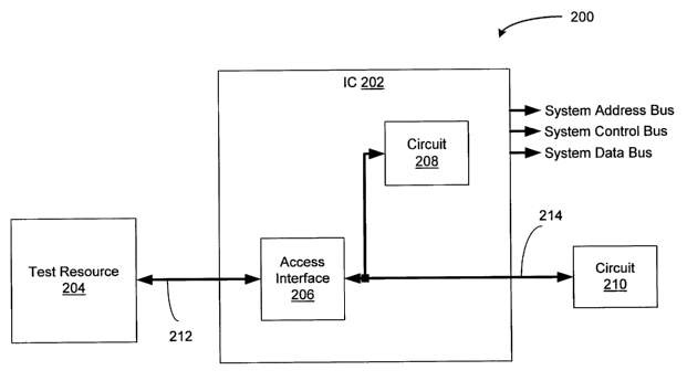
Fig. 2 depicts an illustrative embodiment of a test
configuration 200 operative in a manner according to the
present invention. Specifically, the test configuration
200 includes an access interface 206 that allows
communications between a test resource 204 and electronic
circuits 208 and 210 under test. In this illustrative
embodiment, both the access interface 206 and the
electronic circuit 208 are embedded in an IC 202; and, the
electronic circuit 210 external to the IC 202 is connected
to the access interface 206 and the circuit 208 by way of
a bus 214 coupled to at least one I/0 pin of the IC 202.
Similarly, the test resource 204 is connected to the
access interface 206 by way of a bus 212 coupled to at
least one I/0 pin of the IC 202.
In one embodiment, the IC 202 used to implement the
access interface 206 may be an Application Specific
Integrated Circuit (ASIC). In this case, the access
interface 206 has a fixed configuration, although it may be
configured to access any number or types of circuits such as
electronic circuits 208 or 210. In another embodiment, the
IC 202 used to implement the access interface 206 may be a
programmable device such as an FPGA. In this case, the FPGA
may be programmed to implement the access interface 206 via
CA 02404059 2002-09-20
WO 01/71876 PCT/US01108884
-14-
the test resource 204, and different configurations of the
access interface 206 may be re-programmed into in the FPGA
to access any number or types of circuits. After testing,
debugging, or programming devices coupled to the access
interface 206, the FPGA may be re-programmed to perform its
intended system function.
Those of ordinary skill in this art will appreciate
that other test configurations are possible. For example,
the access interface 206 may be implemented on an IC that
is separate from any IC including circuits under test.
Further, the test resource 204 may alternatively comprise
a programming or debugging resource, and the combination
of the test resource 204 and the access interface 206 may
be used to program or debug the circuits 208 and 210.
The test resource 204 may comprise at least one
memory such as a ROM or RAM, and at least one processor
operative for executing programs stored in the memory,
including applications for communicating with the access
interface 206 to program, test, or debug the circuits 208
and 210. Further, as depicted in Fig. 2, the test
resource 204 may be externally connected to the IC 202
incorporating the access interface 206. Alternatively,
the test resource 204 may be embedded in the IC 202.
It should be understood that the test configuration
200 may include more than one access interface; and, each
access interface may be connected to one or more
electronic circuits such as the embedded circuit 208 and
the external circuit 210.
Fig. 4 depicts an illustrative embodiment of the
access interface 206 that can be used to program, test, or
debug the circuits 208 and 210. Specifically, the access
CA 02404059 2002-09-20
WO 01/71876 PCT/USO1/08884
-15-
interface 206 is connected to a protocol interface 402 and
an Instruction Register (IR) 404. In one embodiment, the
protocol interface 402 comprises the standard TAP
Controller 102 (see Figs. 1 and 3). In a~ preferred
embodiment, the protocol interface 402 is a modified TAP
Controller, which will be described in detail below. In
this illustrative embodiment, the access interface 206,
the modified TAP Controller 402, the IR 404, and
multiplexors 406 and 408 connected thereto, are embedded
in the IC 202 (see Fig. 2) and operatively connected to
the test resource 204 and the circuits 208 and 210.
More specifically, the modified TAP Controller 402 is
connected to the test resource 204 by way of the bus 212,
which is coupled to input pins TRSTN, TMS, and TCK of the
IC 202. Similarly, the access interface 206, the IR 404,
and the multiplexor 406 are connected to the test resource
204 by way of the bus 212, which is also coupled to an
input pin TDI and an output pin TDO. Still further, the
access interface 206 is connected to the circuits 208 and
210 by way of the bus 214, which is coupled to a CONTROL
bus 418, an ADDRESS bus 419, and a bi-directional DATA bus
420.
In this illustrative embodiment, the TDI, TDO, TCK,
and TMS pins correspond to the mandatory pins of the IEEE
1149.1 Standard; and, the TRSTN pin corresponds to the
optional input pin of the IEEE 1149.1 Standard.
Accordingly, registers included in the access interface
206 can serially receive data via the TDI pin, and
serially transmit data on the TDO pin by way of the
multiplexors 406 and 408.
CA 02404059 2002-09-20
WO 01/71876 PCT/USO1/08884
-16-
In addition, the modified TAP Controller 402 includes
conventional circuitry for providing an AI RESET signal on
a line 430 and DR CNTL signals on a bus 432 to the access
interface 206; and, the IR 404 includes conventional
circuitry for providing DR SEL signals on a bus 434 and a
AI ENABLE signal on a line 436 to the access interface
206. Specifically, the DR SEL signals are used to select
a register in the access interface 206; the DR-CNTL
signals are used to control register operations (e. g.,
Capture, Shift, and Update operations) using the selected
register; the AI-RESET signal is used to reset the access
interface 206; and, the AI ENABLE signal is used to enable
the access interface 206. The operation of these signals
will be described in detail below.
As depicted in Fig. 4, the access interface 206
includes a protocol generator 410, which is connected to a
multiplexor 414 for providing control signals in
programmed sequences to the circuits 208 and 210 on the
bus 418. Specifically, the multiplexor 414 receives a
signal from the protocol generator 410 on lines 428 to
select between normal system control signals of the
circuits 208 and 210 on a bus 424 and programmed protocol
signals on a bus 422. In this illustrative embodiment,
the normal system control signals are provided by the IC
202 (see Fig. 2).
Similarly, the protocol generator 410 is connected to
a multiplexor 415 and can be used to provide address
signals in programmed sequences to the circuits 208 and
210 on the bus 419. Specifically, the multiplexor 415
receives a signal from the protocol generator 410 on the
lines 428 to select between normal system address signals
CA 02404059 2002-09-20
WO 01/71876 PCT/USO1/08884
-17-
of the circuits 208 and 210 on a bus 425 and programmed
address signals on a bus 423. In this illustrative
embodiment, the normal system address signals are provided
by the IC 202 (see Fig. 2). The protocol generator 410
further includes a sequence generator 802 comprising a
plurality of registers, e.g., registers SRl through SRN,
and an address register (AR) 804 (see Fig. 8), that are
connected between the TDI and TDO pins.
The access interface 206 also includes a data
generator 412, which includes another plurality of
registers, e.g., a register 601 comprising registers 602
and 604 (see Fig. 6), and separate registers 702 and 704
(see Fig. 7), that are connected between the TDI and TDO
pins. Specifically, the registers of the data generator
412 receive the DR SEL signals from the IR 404 and the
DR CNTL signals from the modified TAP Controller 402 for
use in performing, e.g., Capture, Shift, and Update
operations.
The data generator 412 is connected to a multiplexor
416 for providing data signals to the circuits 208 and 210
on the bus 420. Specifically, the multiplexor 416
receives a signal from the protocol generator 410 on the
lines 428 to select between the data signals generated by
the data generator 412 on bus 426 and normal system data
signals of the circuits 208 and 210 on bus 429. In this
illustrative embodiment, the normal system data signals
are provided by the IC 202 (see Fig. 2).
The registers of the data generator 412 vary in
length depending upon specific applications and numbers of
data inputs and outputs of the circuits 208 and 210. In a
preferred embodiment, the registers of the data generator
CA 02404059 2002-09-20
WO 01/71876 PCT/USO1/08884
-18-
412 include as many cells or bits as there are data inputs
and outputs of the circuits 208 and 210.
The registers of the data generator 412 also provide
specialized data access and/or test functions. For
example, in BIST implementations, the data generator 412
may include a Linear Feedback Shift Register (LFSR) for
providing test stimuli and a Multiple Input Signature
Register (MISR) for capturing a circuit response.
Fig. 5 depicts a state diagram 500 for the FSM of the
modified TAP Controller 402. Specifically, the state
diagram 500 includes eight (8) steady-states, i.e., a
Test-Logic-Reset 502 state, a Run-Test/Idle 504 state, a
Shift-DR 510 state, a Pause-DR 514 state, a Shift-IR 524
state, a Pause-IR 528 state, an Accessl-DR 536 state, and
an Access2-DR 540 state. Further, the state diagram 500
includes a Select-IR branch 503 that defines a sequence of
states for performing an "IR-scan" operation, a Select-DR
branch 501 that defines a sequence of states for
performing ~~DR-scan" operations, and an access interface
branch 505 that defines a sequence of states for
performing programmable access operations using the access
interface 206.
The logic level of the AI-ENABLE signal (initially
logical 0; "AI-ENABLE is low" ) and the logic level at the
TMS pin determine a next state of the modified TAP
Controller 402 FSM, and the clock signal at the TCK pin
~~the TCK clock") causes state transitions to occur.
Specifically, the state diagram 500 shows that the Test-
Logic-Reset 502 state is a steady-state when the level at
the TMS pin is logical 1 (~~TMS is high"). Next, if the
level at the TMS pin changes from logical 1 to logical 0
CA 02404059 2002-09-20
WO 01/71876 PCT/USO1/08884
-19-
(~~TMS is low" ) , then there is a transition from the Test-
Logic-Reset 502 state to the Run-Test/Idle 504 state at
the next rising edge of the TCK clock. The Run-Test/Idle
504 state is a steady-state when TMS is low.
If the level at the TMS pin now changes from low to
high, then there is a transition from the Run-Test/Idle
504 state to the Select-DR-Scan 506 state at the next
rising edge of the TCK clock. As depicted in Fig. 5,
either the Select-DR branch 501 or the access interface
branch 505 can be selected as the next sequence of states
from the Select-DR-Scan 506 state. Otherwise, at the next
rising edge of the TCK clock, there is a transition from
the Select-DR-Scan 506 state to the Select-IR-Scan 520
state. As depicted in Fig. 5, the Select-IR branch 503
can be selected as the next sequence of states from the
Select-IR-Scan 520 state.
Specifically, if the level of the TMS pin changes
from high to low when in the Select-DR-Scan 506 state,
then at the next rising edge of the TCK clock there is a
transition from the Select-DR-Scan 506 state to the
Capture-DR 508 state, which is the first state in the
Select-DR branch 501. Similarly, if the level of the TMS
pin changes from high to low when in the Select-IR-Scan
520 state, then at the next rising edge of the TCK clock
there is a transition from the Select-IR-Scan 520 state to
the Capture-IR 522 state, which is the first state in the
Select-IR branch 503. In this illustrative embodiment,
the state sequences in the Select-DR branch 501 (i.e.,
states 508, 510, 512, 514, 516, and 518) and the Select-IR
branch 503 (i.e., states 522, 524, 526, 528, 530, and 532)
are the same as those in the corresponding Select-DR
CA 02404059 2002-09-20
WO 01/71876 PCT/USO1/08884
-20-
branch 301 and Select-IR branch 303, respectively, of the
standard TAP Controller 102 FSM (see Figs. 1 and 3).
Further, if the level of the TMS pin changes from
high to low and the level of the AI ENABLE signal changes
from low to high ("AI ENABLE is high") when in the Select
DR-Scan 506 state, then at the next rising edge of the TCK
clock there is a transition from the Select-DR-Scan 506
state to an Enter-Access-DR 534 state, which is the first
state in the access interface branch 505. As depicted in
Fig. 5, each branch 501, 503, and 505 of the state diagram
500 is compliant with the IEEE 1149.1 Standard in that the
modified TAP Controller 402 FSM can be reset to the Test-
Logic-Reset 502 state within 5 cycles of the TCK clock
when TMS is high.
As mentioned above, in this illustrative embodiment,
the Select-DR branch 501 and the Select-IR branch 503 of
the state diagram 500 correspond to the Select-DR branch
301 and the Select-IR branch 303, respectively, of the
standard TAP Controller 102 FSM. Accordingly, the
operations performed in the respective state sequences of
the Select-DR branch 501 and the Select-IR branch 503 are
fixed. In contrast, the operations performed in the state
sequence of the access interface branch 505 (i.e., states
534, 536, 538, 540, 542, and 544) are programmable.
For example, the operations performed in the state
sequence of the access interface branch 505 may be
programmed in response to a predetermined event such as
the provision of an electronic circuit with internal scan
registers. Accordingly, the access interface branch 505
may be programmed to generate a repeatable Shift/Capture
CA 02404059 2002-09-20
WO 01/71876 PCTNSO1/08884
-21-
sequence, which may then be used to control operations
using the internal scan registers.
Specifically, if the level of the TMS pin remains low
when in the Enter-Access-DR 534 state, then at the next
rising edge of the TCK clock there is a transition from
the Enter-Access-DR 534 state to the Accessl-DR 536 state.
For example, the Accessl-DR 536 state may be programmed to
perform either a Shift operation on a selected register or
a Pause operation. Further, the Accessl-DR 536 state is a
steady-state when TMS is low.
If the level of the TMS pin changes from low to high
when in the Accessl-DR 536 state, then at the next rising
edge of the TCK clock there is a transition from the
Accessl-DR 536 state to an Updatel/Capturel-DR 538 state.
For example, the Updatel/Capturel-DR 538 state may be
programmed to perform an Update operation only, a Capture
operation only, or both the Update and Capture operations.
Specifically, when the Updatel/Capturel-DR 538 state is
programmed to perform both the Update and Capture
operations, at the next falling edge of the TCK clock
after transitioning to the Updatel/Capturel-DR 538 state,
the Update operation is performed; and, at the next rising
edge of the TCK clock, the Capture operation is performed
followed by a transition from the Updatel/Capturel-DR 538
state to the next state.
If the level of the TMS pin now changes from high to
low, then at the next rising edge of the TCK clock there
is a transition from the Updatel/Capturel-DR 538 state to
the Access2-DR 540 state. Like the Accessl-DR 536 state,
the Access2-DR 540 state may be programmed to perform
either a Shift operation on the selected register or a
CA 02404059 2002-09-20
WO 01/71876 PCT/USO1/08884
-22-
Pause operation. Further, the Access2-DR 540 state is a
steady-state when TMS is low.
If the level of the TMS pin changes from low to high
when in the Access2-DR 540 state, then at the next rising
edge of the TCK clock there is a transition from the
Access2-DR 540 state to an Update2/Capture2-DR 542 state.
Like the Updatel/Capturel-DR 538 state, the
Update2/Capture2-DR 542 state may be programmed to perform
an Update operation only, a Capture operation only, or
both the Update and Capture operations.
Finally, if the level of the TMS pin remains high,
then at the next rising edge of the TCK clock there is a
transition from the Update2/Capture2-DR 542 state to an
Exit-Access-DR 544 state, which is the last state in the
access interface branch 505.
It should be noted that if the level of the TMS pin
changes from low to high when in the Enter-Access-DR 534
state, then at the next rising edge of the TCK clock there
is a transition from the Enter-Access-DR 534 state to the
Updatel/Capturel-DR 538 state. Further, if the level of
the TMS pin remains high when in the Updatel/Capturel-DR
538 state, then at the next rising edge of the TCK clock
there is a transition from the Updatel/Capturel-DR 538
state to the Exit-Access-DR 544 state. Still further, if
the level of the TMS pin changes from high to low when in
the Update2/Capture2-DR 542 state, then at the next rising
edge of the TCK clock there is a transition from the
Update2/Capture2-DR 542 state to the Accessl-DR 536 state.
When AI ENABLE is high, the access interface 206 is
enabled. As a result, subsequent operations are performed
on selected registers included in the access interface
CA 02404059 2002-09-20
WO 01/71876 PCT/USO1/08884
-23-
206. It should be understood that instructions loaded
into the IR 404 not only select the registers in the
access interface 206, but also program the states 536,
538, 540, and 542 of the access interface branch. 505. The
operations are then sequenced as the modified TAP
Controller 402 FSM follows the access interface branch
505. The access interface 206 may have any number of
instructions corresponding thereto, depending upon the
circuits to be accessed and the desired applications.
Specifically, if the instruction loaded into the IR
404 selects a register of the data generator 412 and
programs the Accessl-DR 536 state to perform a Shift
operation, then upon entering the Accessl-DR 536 state,
data in the selected register may be shifted while the
protocol generator 410 concurrently executes a sequence of
access operations on the circuit 208 or 210. Further, the
amount of data shifted and the access sequence length may
be precisely controlled based upon the number of TCK clock
cycles that occurs when in the Accessl-DR 536 state.
Alternatively, the instruction loaded into the IR 404 may
program the Accessl-DR 536 state to perform a Pause
operation only to pause the data generator 412 for a
predetermined number of TCK clock cycles while the
protocol generator 410 concurrently executes. The
Access2-DR 540 state may be programmed in a similar
manner.
The Updatel/Capturel-DR 538 and Update2/Capture2-DR
542 states also allow programmable Update and Capture
operation sequences to occur based upon instructions
loaded into the IR 404. For example, the instruction
loaded into the IR 404 may select a register of the data
CA 02404059 2002-09-20
WO 01/71876 PCT/USO1/08884
-24-
generator 412, program the Updatel/Capturel-DR 538 state
to perform an Update operation, and program the
Update2/Capture2-DR 542 state to perform a Capture
operation using the selected register.
In addition, the Accessl-DR 536 state, the
Updatel/Capturel-DR 538 state, and the Access2-DR 540
state may be similarly programmed to generate a
Shift/Capture/Shift sequence, which may be used to control
operations on internal scan registers. In this way, an
Update operation, which is typically not required for
controlling operations on internal scan registers, can be
eliminated from this sequence.
In addition, both the Updatel/Capturel-DR 538 and
Update2/Capture2-DR 542 states may be programmed to
generate an Update operation immediately followed by a
Capture operation. This Update/Capture sequence makes it
possible to perform path delay testing of interconnects
using standard boundary scan cells.
In addition, the Updatel/Capturel-DR 538 and Access2
DR 540 states may be programmed to generate a
Capture/Shift sequence, which may be used to capture read
data from a memory circuit into a register of the data
generator 412 and then immediately start shifting the read
data out.
In addition, either the Updatel/Capturel-DR 538 state
or the Update2/Capture2-DR 542 state may be programmed to
inhibit both the Update and the Capture operations. As a
result, these states may be used for merely starting,
stopping or continuing execution of the protocol generator
410.
CA 02404059 2002-09-20
WO 01/71876 PCT/USO1/08884
-25-
Upon entering the Exit-Access-DR 544 state, the
access interface 206 is disabled. Further, depending upon
whether TMS is high or low, at the next rising edge of the
TCK clock there may be a transition from the Exit-Access-
DR 544 state to either the Run-Test/Idle 504 state to
"park" the modified TAP Controller 402 or to the Select-
DR-Scan 506 state to start a new operation.
Figs. 6 and 7 depict block diagrams of illustrative
embodiments of the data generator 412. As depicted in
Fig. 6, the data generator 412 includes the register 601
comprising the register 602 for performing Shift/Capture
operations and the register 604 for performing Update
operations. In a preferred embodiment, both the registers
602 and 604 include as many cells as there are data inputs
and outputs in, e.g., the circuits 208 and 210. For
example, the data generator 412 may include a plurality of
registers such as the register 601.
Instructions loaded into the IR 404 are used to
generate (1) the DR_SEL signals for selecting a register
in the data generator 412, e. g. , the register 601, and (2 )
the AI ENABLE signal for enabling operation of the access
interface 206 including the data generator 412. Further,
the modified TAP Controller 402 generates (1) the AI RESET
signal for resetting the access interface 206, and (2) the
DR CNTL signals for controlling the Shift/Capture/Update
operations of the selected register. It should be
understood that the manner in which the registers of the
data generator 412 are enabled, selected, re-set, and
controlled is conventional.
In addition, the register 602 shifts-in data at the
TDI pin and shifts-out data on the TDO pin. Further, the
CA 02404059 2002-09-20
WO 01/71876 PCT/USO1/08884
-26-
timing of the Shift/Capture/Update operations performed by
the register 601 are synchronized with either the TCK
clock or with a system clock of the circuit 208 or 210.
Specifically, the register 601 can be ~ used for
accessing data portions of the circuits 208 and 210 using
simple register operations. For example, the register 602
may capture data from the circuits 208 and 210, and the
register 604 may update data to the circuits 208 and 210.
The Capture operation may be performed following an access
sequence that causes the circuit 208 or 210 to output data
onto parallel inputs 606 of the register 602. That data
can then be latched into the register 602 during, e.g.,
the Updatel/Capturel-DR 538 state of the access interface
branch 505 (see Fig. 5). Next, that data can be serially
shifted-out to the TDO pin during, e.g., the Access2-DR
540 state, so that it can be observed. Further, the
Update operation may be performed by first serially
shifting data into the register 602 during, e.g., the
Accessl-DR 536 state, thereby loading the register 602.
When the Shift operation has completed, that data can be
moved in parallel to the register 604 during, e.g., the
Updatel/Capturel-DR 538 state, for subsequent output to
the circuit 208 or 210 via parallel outputs 610.
As depicted in Fig. 7, the data generator 412
alternatively includes at least two (2) separate registers
connectable to the circuits 208 and 210, e.g., the
register 702 for receiving data from the circuits 208 and
210 on parallel inputs 706 and outputting data to the
circuits 208 and 210 on parallel outputs 708, and the
register 704 for receiving data from the circuits 208 and
210 on parallel inputs 710 and for outputting data to the
CA 02404059 2002-09-20
WO 01/71876 PCT/USO1/08884
-27-
circuits 208 and 210 on parallel outputs 712.
Specifically, the two (2) registers 702 and 704 are on
separate scan paths. The register 702 is scanned using a
first pair of TDI-1-TDO_1 pins; and, the register 704 is
scanned using a second pair of TDI-2-TDO-2 pins. It
should be understood that the manner in which the
registers of the data generator 412 are enabled using the
AI-ENABLE signal, selected using the DR-SEL signals, re
set using the AI-RESET signal, and controlled using the
DR CNTL signals is conventional.
Fig. 8 shows a block diagram of an illustrative
embodiment of the protocol generator 410. Specifically,
the protocol generator 410 includes the sequence generator
802 and the address register 804. The sequence generator
802 provides a programmable way of applying a particular
access protocol to the circuit 208 or 210; and, the
address register 804 provides a programmable way of
applying a sequence of addresses to the circuit 208 or
210.
The sequence register 802 includes a scannable
control queue comprising the registers SR1 through SRN,
which can apply logic levels directly (i.e., in parallel)
to control inputs of the circuit 208 or 210 via the bus
422. Alternatively, the control queue contents may
control or be decoded by additional logic within the
protocol generator 410 to provide control signals to the
circuit 208 or 210. For example, the additional logic may
include a clock generator 810, which outputs a CLOCK
signal on the bus 422. The clock generator 810 may be
used, e.g., to provide an access clock such as the TCK
clock or a system clock to the connected circuit 208 or
CA 02404059 2002-09-20
WO 01/71876 PCT/USO1/08884
-28-
210. Accordingly, the clock generator 810 may include
divider circuitry for setting a specific clock rate, or a
pulse-width shaping circuit for accessing asynchronous
memories using a clock that is synchronous to the access
interface 206. During operation of the access interface
206, this additional logic may synchronize with the TCK
clock or the system clock to allow it to operate at the
system speed of the circuit 208 or 210.
In this illustrative embodiment, the control queue of
the sequence register 802 is N-registers deep by M-bits
wide. For example, the N-register deep control queue may
be configured to support the maximum length protocol
sequence to be applied to the circuit 208 or 210. These N
control queue locations are depicted in Fig. 8 as SRl
through SRN.
Specifically, during operation of the access
interface 206 (i.e., while AI_ENABLE is high), the N
control queue locations are successively accessed and
their contents used to sequence the control signals of the
circuit 208 or 210 via the bus 422, and to control
sequencing of the data generator 412 using DG CNTL signals
on a bus 488 (see also Fig. 4). Accordingly, each control
queue location SR1 through SRN holds values for a single
control state of the circuit 208 or 210 along with
corresponding control states of the data generator 412.
In addition, when operation of the access interface
206 is disabled (i.e., AI ENABLE is low), the contents of
the registers SR1 through SRN can be scanned.
Accordingly, the sequence register 802 can be programmed
to set initial contents of the registers SRl through SRN
before enabling the access interface 206.
CA 02404059 2002-09-20
WO 01/71876 PCT/USO1/08884
-29-
The programmability of the protocol generator 410
permits (1) the sequence length of the access protocol to
vary, e.g., from 1 control sequence up to the maximum
queue depth of N, and (2) the access protocol to be
repetitively applied without re-scanning the contents of
the registers SR1 through SRN. Consequently, the sequence
register 802 can apply various sequences of control
signals in accordance with required circuit access
protocols.
As mentioned above, the control queue locations SRl
through SRN also contain levels for controlling the access
interface 206. As depicted in Fig. 8, the sequence
register 802 provides AR CNTL signals to the address
register 804 via a bus 832, which may be used to select or
control a particular address sequence generated by the
address register 804. The sequence register 802 also
provides the DG-CNTL signals to the data generator 412 on
the bus 830, which may be similarly used to select or
control a particular data sequence generated by the data
generator 412.
The execution of the sequence register 802 is
controlled by SR select logic 806 (see Fig. 8), which
provides control signals to the sequence register 802.
For example, the SR select logic 806 may be programmed via
scan initialization to vary the control queue depth from 1
to N. In a preferred embodiment, when the control queue
depth is programmed to be less than N, upper control queue
locations are not included in the access protocol
sequence. The execution of the sequence register 802
starts based upon an instruction loaded in the IR 404,
which causes the DR-SEL and AI_ENABLE signals to be
CA 02404059 2002-09-20
WO 01/71876 PCTNSO1/08884
-30-
appropriately asserted. During the execution of the
sequence register 802, the SR Select Logic 806 may either
stop sequencing the sequence register 802 after the
programmed number of locations have been executed, or
repeat that sequence until stopped by the modified TAP
Controller 402.
As mentioned above, the address register 804 provides
address sequences to the circuit 208 or 210 via the bus
423. For example, if the circuit 208 or 210 includes a
memory circuit, then the address register 804 may provide
address sequences directly (i.e., in parallel) to the
memory circuit instead of providing the address sequences
via a scan register. As a result, the protocol generator
410 can access memories without having to perform a scan
operation each time a new memory location is to be
accessed.
The address register 804 includes one or more address
generation circuits. For example, these circuits may
include up/down counters or pseudo-random sequence
generators such as an LFSR. Further, each address
generation circuit may comprise a separate address
register within the address register 804. The address
register 804 also includes conventional control circuitry
for the address generation circuits, e.g., to select an up
or down count sequence. The address register 804 can
therefore be configured to support different access
sequences for different types of memories. For example,
the address register 804 may provide multiple address
sequences to support the programming, testing, and
debugging of mufti-ported memories.
CA 02404059 2002-09-20
WO 01/71876 PCT/USO1/08884
-31-
As also mentioned above, the address register 804
receives control inputs from the sequence register 802 via
the AR-CNTL signals. For example, the AR-CNTL signals may
come directly from the sequence register 802 queue or may
alternatively be decoded by the address register 804.
Further, the AR CNTL signals may be used to direct one of
the address generation circuits to advance to a next
memory address. The address register 804 can also control
the SR Select Logic 806 via PG CNTL signals on a bus 834
and control the data generator 412 via the DG CNTL signals
on the bus 488, thereby allowing values or conditional
events included in address sequences to control both
protocol and data generation in the access interface 206.
In this illustrative embodiment, the sequence
register 802 is scannable; and, the address register 804
and the registers SR1 through SRN are included in the same
scan path, which is connected between the TDI and the TDO
pins. Accordingly, the address register 804 can be
scanned along with the sequence register 802. Scanning
the address register 804 allows its address register
contents and any control logic included therein to be
initialized before enabling the access interface 206.
The length of the scan chain including the registers
SR1 through SRN and address register 8C4 depends upon
specific configurations of the address register 804 and
the control queue of the sequence register 802. In this
exemplary embodiment, the sequence register 802 has a
length of (N x M) bits, and the address register 804 has a
length totaling all of the lengths of the address
registers included therein.
CA 02404059 2002-09-20
WO 01/71876 PCT/USO1/08884
-32-
In an alternate embodiment, the sequence register 802
and the address register 804 are partitioned so as to be
on more than one scan path within the protocol generator
410. For example, the (N x M) bits of the sequence
register 802 may be on one scan path, and each register of
the address register 804 may be on separate scan paths.
In this alternate embodiment, the protocol generator 410
may have multiple pairs of TDI-TDO pins. It should be
understood that the manner in which the registers SRl
through SRN and the address register 804 are enabled using
the AI-ENABLE signal, selected using the DR SEL signals,
re-set using the AI-RESET signal, and controlled using the
DR CNTL signals is conventional.
Fig. 9 depicts an illustrative embodiment of a
control queue location 900 included in the sequence
register 802. The queue location 900 indicates various
control field/bit assignments that are representative of
the control required to program, test, or debug, e.g., an
asynchronous SRAM device on a PCB or embedded in an IC.
The three most significant bits (MSBs), i.e., bits 3
through 5, are used to control logic within the protocol
generator 410. Specifically, MSB 5 (SR EOS) is used to
indicate that this ~SR location is the end of the protocol
sequence by signaling the SR Select Logic 806 to stop the
control queue sequencing at this point. Further, bit 4
(AR Next) is used to direct the address register 804 to
advance to a next memory address; and, bit 3 (DG Next) is
used to direct the data generator 412 to generate a next
data pattern, e.g., a foreground or background data
pattern in the case of a memory BIST application.
CA 02404059 2002-09-20
WO 01/71876 PCT/USOI/08884
-33-
As depicted in Fig. 9, the three least significant
bits (LSBs) of the queue location 900 are control signals
that can be directly applied to the circuit 208 or 210.
For example, the circuit 208 or 210 may comprise an SRAM.
Accordingly, bit 2 (CEN) is a chip enable signal, bit 1
(OEN) is an output enable signal, and LSB 0 (WEN) is a
write enable signal for the exemplary SRAM device. By
setting values for CEN, OEN and WEN in respective control
queue locations, the access sequence for the SRAM can be
programmed to perform, e.g., a read operation, a write
operation, a read followed by a write operation, etc.
Fig. 9 depicts the TDI and TDO pin connections
relative to the single queue location 900. In this
illustrative embodiment, these TDI and TDO pin connections
are chained from one queue location to the next for the
entire sequence register 802 to place the registers SR1
through SRN on the same scan path.
In one embodiment, the queue location 900 may be
shared and used to access other circuits in addition to
the SRAM mentioned above. Because the sequence register
802 is programmable, the control queue bits can be
redefined to accommodate requirements of the multiple
circuits. Further, additional control queue bits may be
defined if needed, e.g., when certain control bits are
used with one circuit and unused for another circuit.
Accordingly, the protocol generator 802 and the data
generator 804 can be configured to support any circuit
coupled to the access interface 206. For example, the
access interface 206 may be connected and dedicated to a
single circuit, or it may be implemented such that it is
shared to provide access to a plurality of connected
CA 02404059 2002-09-20
WO 01/71876 PCT/USO1/08884
-34-
circuits such as the circuits 208 and 210. The access
interface 206 may also be partitioned among a plurality of
circuits and/or devices. For example, the data generator
412 may be shared between a group of memories .while using
separate protocol generators 802, each one dedicated for
use with a respective memory. This would allow, e.g., a
different BIST algorithm for each memory to be programmed
in corresponding protocol generators, and the different
BIST algorithms to be executed concurrently using the
access interface 206.
Alternatively, a plurality of access interfaces may
operate in parallel from a single TAP Controller 402, or a
single access interface may be partitioned across multiple
ICs and synchronized to run from multiple TAP controllers
402. For example, this configuration may be used when an
external memory structure is connected to multiple ASICs
on a PCB, with a first ASIC controlling a memory data bus
and a second ASIC providing address and control signals to
the memories. In this application, the access interface
206 may be partitioned so that the data generator 412 is
implemented in the first ASIC and the protocol generator
410 is implemented in the second ASIC. Each ASIC would
then have a TAP Controller that would be used to run the
access interface 206 partitioned across the two ASICs.
The embodiments disclosed herein will be better
understood with reference to the following illustrative
examples. In a first illustrative example, a memory
circuit having 8-bits of input data and 8-bits of output
data is connected to the access interface 206, which
accesses this memory circuit using the data generator 412,
as depicted in Fig. 6. Specifically, the data generator
CA 02404059 2002-09-20
WO 01/71876 PCT/USO1/08884
-35-
412 is implemented as dedicated logic using eight (8) BSR-
type cells, and therefore has a scan length of 8-bits. In
this first illustrative example, a Capture operation is
used during memory read operations to capture. data read
from the memory into the data generator 412 on the inputs
606. The test resource 204 (see Fig. 2) then scans the 8-
bits of captured data, which is read out of the data
generator 412 on the TDO pin of the device, to observe the
accessed memory data. Similarly, memory write data may be
scanned into the data generator 412; and, following an
Update operation, a programmed access sequence of the
protocol generator 410 may write this byte of data to the
memory on the outputs 610.
In a second illustrative example, the access
interface 206 of Fig. 12 is used to access an external
SRAM memory device. For example, the circuitry depicted
in Fig. 12 may be implemented inside an ASIC or programmed
in an FPGA, and that device may be connected to the
external SRAM on a PCB.
The access interface 206 of Fig. 12 includes the
sequence register 802, the address register 804, and the
data generator 412. In this second illustrative example,
the multiplexors 414, 415, and 416 that select between the
normal system signals and the signals generated by the
access interface 206 are not explicitly shown.
Specifically, the multiplexors 414, 415, and 416 are
implemented with logic external to the access interface
206 but inside the same device containing the TAP
Controller 402 and the access interface 206. The access
interface 206 provides a signal on the lines 428 to select
between the signals at the inputs of the multiplexors 414,
CA 02404059 2002-09-20
WO 01/71876 PCT/USO1/08884
-36-
415, and 416. The access interface 206 also provides
ADDRESS signals on the bus 419, and a set of CONTROL
signals, i.e., CEN, OEN and WEN, on the bus 418. These
control signals are the same as those indicated in bits 0
through 2 of the queue location 900 (see Fig. 9). Data
passing between the external SRAM and the data generator
412 on the bus 420 are also depicted in Fig. 12. All of
the signals transmitted to and received from the memory
are selected at the multiplexors 414, 415, and 416. These
signals will be selected and connected to corresponding
data, address, and control terminals of the SRAM during
operation of the access interface 206.
In a third illustrative example, the access interface
206 of Fig. 13 is used to access a serial EEPROM device.
The circuitry depicted in Fig. 13 may also be implemented
inside an ASIC or programmed in an FPGA, and that device
may be connected to the serial EEPROM device on a PCB.
The TAP Controller 402 of Fig. 13 is identical to
that of Fig. 12. However, in this example the scan logic
has been adapted for accessing the serial EEPROM device.
Further, the access interface 206 of Fia. 13 shows only
the sequence register 802 and the clock generator 810.
The address register 804 and the data generator 412 are
not explicitly shown because in this example they are not
required for accessing the serial EEPROM device.
As in the SRAM example relating to Fig. 12, the
access interface 206 generates control signals, i.e., CSN,
HOLDN, and SCK, on the bus 418 to the serial EEPROM
device. These signals enable chip operations and provide
for clocking of the serial EEPROM device. The access
interface 206 of Fig. 13 also provides select signals on
CA 02404059 2002-09-20
WO 01/71876 PCT/USO1/08884
-37-
the lines 428, as in the second illustrative example.
However, address and data signals for reading from and
writing to the memory are accessed as a specific serial
I/0 protocol via the TDI-TDO pins, which in this
illustrative example are coupled to both of the buses 212
and 214. Because the serial I/O protocol may be sent
directly via the TDI-TDO pins, the address register 804
and the data generator 412 are not needed. The serial I/O
protocol will vary depending on the size of the serial
EEPROM device connected to the access interface 206. For
example, for smaller devices the serial address may be 10-
bits long, and for larger devices up to 17-bits of serial
address may be provided. The clock generator 810 of Fig.
13 provides an access clock signal, SCK, which is divided
down from the TCK clock. A programmable clock divider
circuit is provided within the clock generator 810 to
accommodate a variety of SCK clock frequencies.
A first method of operation of the access interface
206 is illustrated by reference to Figs. 10 and 14.
Specifically, the timing diagram of Fig. 10 and the flow
diagram of Fig. 14 depict the timing and software flow,
respectively, for a typical series of memory access
operations, e.g., a read operation, immediately followed
by a write operation, and immediately followed by another
read operation. Before the memory access operations are
performed, the access interface 206 is initialized as
follows. First, the modified TAP Controller 402 is reset,
as depicted in step 1402 (see Fig. 14), thereby placing
the modified TAP Controller 402 in the Test-Logic-Reset
502 state. This also causes the AI RESET signal to be
asserted, thereby resetting the access interface 206.
CA 02404059 2002-09-20
WO 01/71876 PCT/USO1/08884
-38-
Next, as depicted in step 1404, a Shift instruction is
loaded into the IR 404 for use in scanning in via the TDI
pin a suitable read/write/read control protocol into the
sequence register 802 and initializing the address
register 804 with a starting address. A memory access
instruction is then loaded, as depicted in step 1406, into
the IR 404 to assert the AI ENABLE signal, program the
Accessl-DR 536 state to perform a Shift operation, program
the Updatel/Capturel-DR 538 state to perform an Update
operation and a Capture operation, program the Access2-DR
540 state to perform a Shift operation, program the
Update2/Capture2-DR 542 state to inhibit both the Update
and Capture operations, and select a register in the data
generator 412. Next, the level of TMS is set to logical
0, as depicted in step 1408, to transition the modified
TAP Controller 402 FSM first to the Enter-Access-DR 534
state and then to the Accessl-DR 536 state (see Figs. 5
and 10). Scan-in data is then shifted, as depicted in
step 1410, via the bus 420 into the selected register of
the data generator 412 from the memory location pointed to
by the starting address; and, a first read control
sequence is concurrently applied, as also depicted in step
1410, via the bus 418 to the memory circuit connected to
the access interface 206. As depicted in the timing
diagram of Fig. 10, four (4) cycles of the TCK clock occur
during the first read operation to shift four ( 4 ) bits of
data into the selected register of the data generator 412
from the memory circuit. The level of TMS is then set, as
depicted in step 1412, to logical 1 to transition the
modified TAP Controller 402 FSM to the Updatel/Capturel-DR
538 state (see Figs. 5 and 10). Next, the shifted data is
CA 02404059 2002-09-20
WO 01/71876 PCT/USO1/08884
-39-
updated, as depicted in step 1414, in the selected
register so that it can be written to the memory circuit
in the next access sequence. It should be noted that the
initial scan-out data, which was shifted-out of the data
generator 412 at the TDO pin, is unknown data and may be
discarded. Next, previously read data is captured, as
depicted in step 1415, in the selected register via the
bus 420 from the memory circuit. Such previously read
data is subsequently shifted out of the data generator 412
via the bus 212. The level of TMS is then set to logical
0, as depicted in step 1416, to transition the modified
TAP Controller 402 FSM to the Access2-DR 540 state (see
Figs. 5 and 10). Next, the data in the selected register
is shifted, as depicted in step 1418, out of the data
generator 412 via the bus 420 to the memory; and, the
protocol generator 410 concurrently applies, as also
depicted in step 1418, a write control sequence via the
bus 418 to the memory and an address control sequence via
the AR CNTL signals to the address register 804 to
increment the stored address. The level of TMS is then
set to logical l, as depicted in step 1420, to transition
the modified TAP Controller 402 FSM to the
Update2/Capture2-DR 542 state (see Figs. 5 and 10),
thereby ending the write operation. Next, a decision is
made, as depicted in step 1422, as to whether the second
memory read sequence has been performed. If not, then the
method loops back to step 1408, thereby starting the
second memory read sequence. Otherwise, the level of TMS
is set to logical 1 and then to logical 0, as depicted in
step 1424, to transition the modified TAP Controller 402
FSM first to the Exit-Access-DR 544 state and then to the
CA 02404059 2002-09-20
WO 01/71876 PCT/USO1/08884
-40-
Run-Test/Idle 504 state (see Figs. 5 and 10), thereby
ending the read/write/read sequence. It should be noted
that the above-described method may be suitably modified
for performing any desired number of memory read/write
operations.
A second method of operation of the access interface
206 is illustrated by reference to Figs. 11 and 15.
Specifically, the timing diagram of Fig. 11 and the flow
diagram of Fig. 15 depict the timing and software flow,
respectively, for a memory access sequence that scans in
an initial data value into the data generator 412,
executes a control protocol sequence using the control
queue of the sequence register 802 that repeatedly
executes a sequence of memory read/write operations, and
finally scans out a data result using the data generator
412. This exemplary sequence may be used to execute a
memory BIST algorithm. First, the modified TAP Controller
402 is reset, as depicted in step 1502 (see Fig. 15), to
place the modified TAP Controller 402 in the Test-Logic-
Reset 502 state. This also causes the AI-RESET signal to
be asserted, thereby resetting the access interface 206.
Next, a Shift instruction is loaded, as depicted in step
1504, into the IR 404 for use in loading the control queue
of the sequence register 802 with the BIST control
protocol and initializing the address register 804 with a
starting address. A memory BIST instruction is then
loaded, as depicted in step 1506, into the IR 404 to set
the AI ENABLE signal high, program the Accessl-DR 536
state to perform a Shift operation, program the
Updatel/Capturel-DR 538 state to perform an Update
operation, program the Access2-DR 540 to perform a memory
CA 02404059 2002-09-20
WO 01/71876 PCT/USO1/08884
-41-
BIST sequence, program the Update2/Capture2-DR 542 state
to perform a Capture operation, and select a register in
the data generator 412. The memory BIST sequence
performed by the Access2-DR 540 will be described in
detail below. Next, the level of TMS is set to logical 0,
as depicted in step 1508, to transition the modified TAP
Controller 402 FSM first to the Enter-Access-DR 534 state
and then to the Accessl-DR 536 state (see Figs. 5 and 11).
Scan-in data is then shifted, as depicted in step 1510,
via the TDI pin into the selected register of the data
generator 412 for use in initializing the register for a
first BIST sequence. It should be noted that in this
exemplary method, a memory control sequence does not start
concurrently with the data generator 412 Shift operation.
Next, the level of TMS is set to logical 1, as depicted in
step 1512, to transition the modified TAP Controller 402
FSM to the Updatel/Capturel-DR 538 state (see Figs. 5 and
11). The shifted data is then updated, as depicted in
step 1514, in the selected register. Next, the level of
TMS is then set to logical 0, as depicted in step 1516, to
transition the modified TAP Controller 402 FSM to the
Access2-DR 540 state (see Figs. 5 and 11) to execute the
memory BIST sequence. This may take many cycles of the
TCK clock to complete. Specifically, in a typical memory
BIST sequence, the data stored in the selected register is
written to a memory location, read back from that
location, and then written to and read back from
successive memory locations until the test is completed.
Accordingly, the address stored in the address register
804 is suitably incremented (or decremented), as further
depicted in step 1516, and the sequence register 802 is
CA 02404059 2002-09-20
WO 01/71876 PCT/USO1/08884
-42-
sequenced and looped, as still further depicted in step
1516, on memory read/write commands based upon the
programming performed in steps 1504 and 1506. Next, the
level of TMS is set to logical l, as depicted in step
1518, to transition the modified TAP Controller 402 FSM to
the Update2/Capture2-DR 542 state. The result of the
memory BIST sequence is then captured, as depicted in step
1519, in the selected register (see Figs. 5 and 10). A
decision is then made, as depicted in step 1520, as to
whether there is any more data to scan into the selected
register of the data generator 412. If so, then the
method loops back to step 1508. As depicted in Fig. 11,
there is valid data at both the TDI and TDO pins during
the subsequent execution of the step 1510. The valid TDO
data is the result of the first memory BIST sequence, and
the valid TDI data is new scan data to be used in a next
memory BIST sequence. Otherwise, if there is no more data
to be scanned into the data generator 412, then another
decision is made, as depicted in step 1522, as to whether
the control queue of the sequence register 802 is to be
loaded with another BIST control protocol. If so, then
the method loops back to step 1504. Otherwise, the level
of TMS is first set to logical 1 and then to logical 0, as
depicted in step 1524, to transition the modified TAP
Controller 402 FSM first to the Exit-Access-DR 544 state
and then to the Run-Test/Idle 504 state (see Figs. 5),
thereby ending the memory BIST sequence. In this
exemplary method, the memory BIST sequence may be repeated
with new data in the selected register, or the modified
TAP Controller 402 FSM may transition to the Exit-Access-
DR 544 state and the sequence register 802 and the address
CA 02404059 2002-09-20
WO 01/71876 PCT/USO1/08884
-43-
register 804 re-initialized to start a new memory BIST
sequence.
Having described the above illustrative embodiments,
other alternative embodiments or variations may be made.
Specifically, Figs. 6 and 7 depict two (2) representative
implementations of the data generator 412. However, the
access interface 206 is intended to support many different
implementations of the data generator 412, depending upon
the specific application, e.g., programming, testing, or
debugging, and the design and type of circuit connected to
it.
Specifically, it was mentioned above that it is
possible for the data generator 412 to operate as a
pattern generator, a comparator, or a signature register
in order to support BIST of a circuit coupled to the
access interface 206. For example, in a BIST
implementation of the data generator 412, the Shift/From
register 702 (see Fig. 7) may be designed to function as
an MISR and the Shift/To register 704 (see Fig. 7) may be
designed to function as an LFSR. Further, although two
(2) separate scan paths are shown in Fig. 7, these scan
paths may be connected to form a single scan path as
depicted in Fig. 7 by the dashed line connecting TDO 1 and
TDI 2. In this application, the TDO 1 output and TDI 2
input are not included in the data generator 412, and
there is only a single TDI-TDO path, as depicted in Fig.
6.
It should also be noted that the data generator 412
allows for asymmetrical data to be sent to and received
from the connected circuit. For example, the single
register data generator 412, as depicted in Fig. 6, may be
CA 02404059 2002-09-20
WO 01/71876 PCT/USO1/08884
-44-
connected to a circuit in which the number of outputs is
not equal to the number of inputs. In this application,
the shift-out/shift-in data for Capture and Update
operations may be appropriately "padded" or masked.
In addition, it was described that the TAP Controller
402 is preferably a modified TAP Controller that not only
includes the standard Select-DR and Select-IR branches 501
and 503, but also includes a new access interface branch
505 with states for implementing operations using the
access interface 206. However, this was merely an
illustrative example. The TAP Controller 402 FSM may
alternatively consist of the standard FSM, as depicted in
Fig. 3. The access interface 206 may therefore optionally
include decode logic 490 (see Fig. 4) for decoding the
states included in the access interface branch 505.
Specifically, the decode logic 490 receives the standard
FSM states and the logic level on the TMS pin as inputs;
and, provides DR CNTL2 signals in place of the DR CNTL
signals to control register operations.
Those of ordinary skill in this art will also
appreciate that variations to and modification of the above-
described apparatus and method for accessing electrical
nodes of electronic circuits may be made without departing
from the inventive concepts disclosed herein. Accordingly,
the present invention should be viewed as limited solely by
the scope and spirit of the appended claims.