Note: Descriptions are shown in the official language in which they were submitted.
CA 02404473 2002-09-27
WO 01/73490 PCT/USO1/07825
OPTICAL SWITCHING SYSTEM WITH POWER BALANCING
FIELD AND BACKGROUND OF THE INVENTION
The present invention relates to the switching of optical signals and, more
particularly, to an optical switching system that facilitates output power
balancing.
In an optical communication network based on Dense Wavelength Division
Multiplexing, signals carried on carrier waves of different wavelengths are
liable to
1o have different optical powers, for several reasons. One reason is that such
a network
uses optical amplifiers to maintain signal power. The optical gain of an
optical
amplifier is not flat, as a function of wavelength. Therefore, even if the
incoming
multiplexed signals are equal in power, the outgoing multiplexed signals
generally are
not equal in power. A second reason is that the multiplexed signals typically
have
different origins, and so have suffered different propagation losses, as a
result of
having traveled different distances, by the time these signals reach an
optical
amplifier. If the range of signal powers among the multiplexed signals
entering an
optical amplifier is too great, the amplifier becomes saturated, resulting in
unacceptable data loss.
Two different approaches have been used to solve this problem. The first
approach is to flatten the response curve of the system (which is a composite
of the
response curves of the optical amplifier and of any other wavelength-dependent
component, such as filters) by introducing a loss curve that is reciprocal to
the
response curve. This can be done passively (Y. Li, "A waveguide EDFA gain
equalizer filter", Electronics Letters, vol. 31 pp. 2005-2006, 1995) or
dynamically (M.
C. Parker, "Dynamic holographic spectral equalization for WDM", IEEE Photon
Technology Letters, vol. 9 pp. 529-531, 1997; J. E. ford and J. A. Walker,
"dynamic
spectral power equalization using micro-opto mechanics", IEEE Photon
Technology
Letters, vol. 10 pp. 1440-1442, 1998). In this approach, the signals remain
3o multiplexed on a common optical waveguide. The second approach
demultiplexes the
signals to respective channels and attenuates each channel using an optical
attenuator.
CA 02404473 2002-09-27
WO 01/73490 PCT/USO1/07825
2
Optical switches such as 2x2 and 1 x2 Mach-Zehnder interferometers can be
used as attenuators. Figure 1 shows a Mach-Zehnder interferometer 10.
Interferometer 10 is based on two more-or-less parallel waveguides, an upper
waveguide 12 and a lower waveguide 14. Waveguides 12 and 14 are coupled to
each
other in a first 3dB directional coupler 16 and in a second 3dB directional
coupler 18.
In-between directional couplers 16 and 18, each waveguide 12 and 14 passes
through
a respective phase shifter 20 and 22. Left end 24 of upper waveguide 12 serves
as an
input port of interferometer 10. Right end 26 of upper waveguide 12 serves as
an
output port of interferometer 10. Right end 28 of lower waveguide 14 is an
idle port.
The operation of interferometer 10 is as follows. Coherent light entering
interferometer 10 at input port 24 is split by,directional coupler 16, with
half the light
continuing rightward in upper waveguide 12 and the other half of the light
propagating rightward in lower waveguide 14. Phase shifters 20 and 22 are used
to
change the relative phases of the light in waveguides 12 and 14. Directional
coupler
18 then causes some or all of the light to emerge from interferometer 10 via
output
port 26 and/or idle port 28, depending on the phase difference, between the
light in
upper waveguide 12 and the light in lower waveguide 14, that is induced by
phase
shifters 20 and 22.
Figure 2 shows the power leaving a specific Mach-Zehnder interferometer 10
2o via output port 28, relative to the power entering this interferometer 10
via input port
24, in dB, versus the heating power applied to either phase shifter 20 or
phase shifter
22. This specific Mach-Zehnder interferometer 10 was fabricated using Si02 on
Si
technology, for light of a wavelength of 1.55 microns. Maximum attenuation, of
35dB, is obtained at point I (approximately 50 mW heating power). Minimum
attenuation is obtained at point II (approximately 610 mW heating power). This
Mach-Zehnder interferometer 10 therefore is capable of a 35dB attenuation
range.
When this Mach-Zehnder interferometer 10 is used as a switch, point I
corresponds to
the switch being OFF, with almost all power leaving the switch via output port
26,
and point II corresponds to the switch being fully ON, with almost all power
leaving
3o the switch via output port 28.
CA 02404473 2002-09-27
WO 01/73490 PCT/USO1/07825
3
The resolution of the attenuation depends on the resolution of the heating
power used in phase shifters 20 and 22.
SUMMARY OF THE INVENTION
2x2 and 1x2 optical switches also are used as elements in optical switch
matrices, such as those taught in PCT application WO 99/60434 and co-pending
US
patent application 09/696,224, for switching optical signals from input
waveguides to
output waveguides. The present invention is an optical switching system based
on an
optical switch matrix that combines the switching functionality of optical
switches
1 o such as Mach-Zehnder interferometer 10 with the attenuation functionality
of such
optical switches in a single unit.
Therefore, according to the present invention there is provided an optical
switching system, for switching optical energy from a plurality of input
waveguides to
a plurality of output waveguides, including: (a) for each output waveguide:
for each
input waveguide: at least one respective attenuator for diverting an
adjustable portion
of the optical energy entering via the each input waveguide to the each output
waveguide.
Furthermore, according to the present invention there is provided a method of
switching each of a plurality of optical signals, that travel on respective
input
2o waveguides, from the respective input waveguide thereof to a desired one of
a
plurality of output waveguides, including the steps of: (a) providing an
optical switch
matrix including: for each output waveguide: for each input waveguide: at
least one
respective attenuator for diverting an adjustable portion of the signal that
travels on
the each input waveguide to the each output waveguide; (b) selecting the
attenuators
that divert the optical signals to the desired output waveguides; and (c)
adjusting the
selected attenuators to balance powers of the optical signals in the output
waveguides.
The optical switching system of the present invention is based on an optical
switch matrix that includes, for each input waveguide and for each output
waveguide,
a set of one or more optical switches for diverting an adjustable portion of
the optical
3o energy in the input waveguide to the output waveguide. At least one of the
optical
switches in each set is an attenuator, preferably a Mach-Zehnder attenuator.
CA 02404473 2002-09-27
WO 01/73490 PCT/USO1/07825
4
Preferably, the switches are 2x2 switches. If there are two switches per set,
one for
input and the other for output, then the input switch has an idle input port
and the
output switch has an idle output port. The input switch of the last switch set
of each
input waveguide also has an idle output port, and the output switch of the
first switch
set of each output waveguide also has an idle input port.
Preferably, the optical switching system of the present invention includes a
feedback mechanism for adjusting the attenuators to balance the output powers
in the
output waveguides. The feedback mechanism includes a power measurement device
such as a spectrum analyzer, a set of taps for diverting fixed portions of the
optical
l0 energy from either the input waveguides or the output waveguides to the
spectrum
analyzer, and a control unit that receives signals from the spectrum analyzer
that
indicate the power levels in the tapped waveguides and that adjusts the
attenuators on
the basis of these signals. Most preferably, each tap includes a directional
coupler that
is coupled to a respective input or output .waveguide.
By "balancing" the output powers in the output waveguides is meant adjusting
the output powers in the output waveguides to facilitate the accurate
transmission of
signals downstream from the optical switching system. Usually, this balancing
is
done by equalizing the powers in all the output waveguides; but there are
circumstances in which the powers are balanced by adjusting them to have
mutual
2o ratios not equal to unity. For example, some of the signals may be destined
for
respective destinations that are farther downstream than other signals. If the
powers
of all the signals are equalized, then, because signal attenuation varies in
the same
sense as distance traveled, the signals with distant destinations arrive at
their
destinations with lower powers than the signals with nearby destinations. In
that case,
it often is desirable to adjust the powers of the signals with distant
destinations to
higher levels than the powers of the signals with nearby destinations, so that
all the
signals arrive at their respective destinations with equal powers.
BRIEF DESCRIPTION OF THE DRAWINGS
3o The invention is herein described, by way of example only, with reference
to
the accompanying drawings, wherein:
CA 02404473 2002-09-27
WO 01/73490 PCT/USO1/07825
FIG. 1 illustrates a Mach-Zehnder interferometer;
FIG. 2 shows relative output power, as a function of applied heating power,
for
one particular Mach-Zehnder interferometer;
FIG. 3 illustrates the architecture of an optical switch matrix of the present
5 invention;
FIG. 4 illustrates the architecture of another optical switch matrix of the
present invention;
FIG. 5 is a high level block diagram of a complete system of the present
invention;
l0 FIG. 6 is a high level block diagram of another complete system of the
present
invention .
DESCRIPTION OF THE PREFERRED EMBODIMENTS
The present invention is of an optical switching system that can be used to
switch optical signals from input waveguides to output waveguides while
balancing
power in the output waveguides.
The principles and operation of an optical switching system according to the
present invention may be better understood with reference to the drawings and
the
accompanying description.
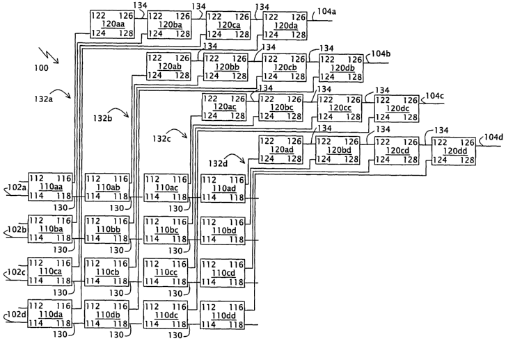
Referring again to the drawings, Figure 3 illustrates the architecture of an
optical switch matrix 100 of the present invention that resembles the optical
switch
matrices taught in WO 99//60434. Optical switch matrix 100 connects four input
waveguides 102 to four output waveguides 104. For this purpose, optical switch
matrix 100 includes sixteen input attenuators 110 and sixteen output
attenuators 120.
Each attenuator 110 or 120 is a Mach-Zehnder interferometer that is
substantially
identical to Mach-Zehnder interferometer 10. Each input attenuator 110 has an
upper
input port 112, a lower input port 114, an upper output port 116 and a lower
output
port 118. Similarly, each output attenuator 120 has an upper input port 122, a
lower
input port 124, an upper output port 126 and a lower output port 128. Each
input
3o waveguide 102 is coupled to each output waveguide 104 by a respective input
attenuator 110 and a respective output attenuator 120. The input attenuator
110 and
CA 02404473 2002-09-27
WO 01/73490 PCT/USO1/07825
6
the output attenuator 120 that couple a particular input waveguide 102 to a
particular
output waveguide 104 are labeled by the corresponding letters: input
attenuator 110aa
and by output attenuator 120aa couple input waveguide 102a to output waveguide
104a, input attenuator 110ab and output attenuator 110ab couple input
waveguide
102a to output waveguide 102b, etc.
More specifically, input waveguides 102 lead into lower input ports 114 of
input attenuators 110 that couple to output waveguide 104a, and output
waveguides
104 emerge from upper output ports 126 of output attenuators 120 that couple
to input
waveguide 102d. Each input attenuator 110 is coupled to its respective output
attenuator 120 by a respective intermediate waveguide 132 that leads from
upper
output port 116 of that input attenuator 110 to lower input port 124 of that
output
attenuator 120. All upper input ports 112 of input attenuators 110 are idle.
Similarly,
all lower output ports 128 of output attenuators 120 are idle. Lower output
ports 118
of input attenuators 110 that couple to output waveguide 104d are idle; and a
respective intermediate waveguide 130 leads from lower output port 118 of each
of
the other input attenuators 110 to lower input port 114 of input attenuator
110 that
couples the same input waveguide 102 to the next output waveguide 104.
Similarly,
upper input ports 122 of output attenuators 120 that couple to input waveguide
102a
are idle; and a respective intermediate waveguide 134 leads to upper input
port 122 of
each of the other output attenuators 120 from upper output port 126 of output
attenuator 120 that couples the same output waveguide 104 to the preceding
input
waveguide 102. As in Mach-Zehnder interferometer 10, lower input port 114 and
lower output port 118 of each input attenuator 110 actually are opposite ends
of the
same internal lower waveguide, and upper input port 122 and upper output port
126 of
each output attenuator 120 actually are opposite ends of the same internal
upper
waveguide, so that intermediate waveguides 130 actually are extensions of
respective
input waveguides 102 and intermediate waveguides 134 actually are extensions
of
respective output waveguides 104.
Each attenuator 110 or 120 is considered OFF in its pass-through state (point
I
in Figure 2), in which all optical energy entering via upper input port 112 or
122
leaves via upper output port 116 or 126, and in which all optical energy
entering via
CA 02404473 2002-09-27
WO 01/73490 PCT/USO1/07825
7
lower input port 114 or 124 leaves via lower output port 118 or 128. With all
attenuators OFF, all optical energy that enters matrix 100 via input
waveguides 102 is
discarded at idle output ports 118. Turning ON the input attenuator 110 and
the
output attenuator 120 that couple a particular input waveguide 102 to a
particular
s output waveguide 104, by increasing the heating power applied to the phase
shifters of
these attenuators 110 and 120 towards point II of Figure 2, diverts some or
all of the
optical energy that enters via that input waveguide 102 to that output
waveguide 104.
Figure 4 illustrates the architecture of another optical switch matrix 200 of
the
present invention that resembles the optical switch matrix taught in US patent
to application no. 09/696,224. Optical switch matrix 200 connects four input
waveguides 202 to four output waveguides 204. For this purpose, optical switch
matrix 200 includes sixteen input attenuators 210 and sixteen output
attenuators 220.
Each attenuator 210 or 220 is a Mach-Zehnder interferometer that is
substantially
identical to Mach-Zehnder interferometer 10. Each input attenuator 210 has an
upper
15 input port 212, a lower input port 214, an upper output port 216 and a
lower output
port 218. Similarly, each output attenuator 220 has an upper input port 222, a
lower
input port 224, an upper output port 226 and a lower output port 228. Each
input
waveguide 202 is coupled to each output waveguide 204 by a respective input
attenuator 210 and a respective output attenuator 220. The input attenuator
210 and
2o the output attenuator 220 that couple a particular input waveguide 202 to a
particular
output waveguide 204 are labeled by the corresponding letters: input
attenuator 210ad
and output attenuator 220ad couple input waveguide 202a to output waveguide
204d,
input attenuator 210ba and output attenuator 210ba couple input waveguide 202b
to
output waveguide 204a, etc.
25 More specifically, input waveguides 202 lead into upper input ports 212 of
input attenuators 210 that couple to the cyclically preceding output
waveguides 204:
input waveguide 202a leads into upper input port 212 of input attenuator
210ad, input
waveguide 202b leads into upper input port 212 of input attenuator 210ba,
input
waveguide 202c leads into upper input port 212 of input attenuator 210cb and
input
30 waveguide 202d leads into upper input port 212 of input attenuator 210dc.
Output
waveguides 204 emerge from upper output ports 226 of output attenuators 220
that
CA 02404473 2002-09-27
WO 01/73490 PCT/USO1/07825
8
couple to the corresponding input waveguides 202: output waveguide 204a
emerges
from upper output port 226 of output attenuator 220aa, output waveguide 204b
emerges from upper output port 226 of output attenuator 220bb, output
waveguide
204c emerges from upper output port 226 of output attenuator 220cc and output
waveguide 204d emerges from upper output port 226 of output attenuator 220dd.
Each input attenuator 210 is coupled to its respective output attenuator 220
by a
respective intermediate waveguide 232 that leads from lower output port 218 of
that
input attenuator 210 to lower input port 224 of that output attenuator 220.
All lower
ports 214 of input attenuators 210 are idle. Similarly, all lower output ports
228 of
output attenuators 220 are idle. Upper output ports of input attenuators
210aa, 210bb,
210cc and 210dd, that couple input waveguides 202 to corresponding output
waveguides 204, are idle. A respective intermediate waveguide 230 leads from
upper
output port 216 of each of the other input attenuators 210 to upper input port
212 of
input attenuator 210 that couples the same input waveguide 202 to the
cyclically
preceding output waveguide 204. For example, an intermediate waveguide 230
leads
from upper output port 216 of input attenuator 210cb to upper input port 212
of input
attenuator 210ca, another intermediate waveguide 230 leads from upper output
port
216 of input attenuator 210ca to upper input port 212 of input attenuator
210cd, and
yet another intermediate waveguide 230 leads from upper output port 216 of
input
2o attenuator 210cd to upper input port 212 of input attenuator 210cc. Upper
input ports
222 of output attenuators 220ad, 220ba, 220cb and 220dc, that couple input
waveguides 202 to cyclically preceding output waveguides 204, are idle. A
respective
intermediate waveguide 234 leads to upper input port 222 of each of the other
output
attenuators 220 from upper output port 226 of output attenuator 220 that
couples the
same output waveguide 204 to the cyclically preceding input waveguide 202. For
example, an intermediate waveguide 234 leads to upper input port 222 of output
attenuator 220ac from upper output port 226 of output attenuator 220dc,
another
intermediate waveguide 234 leads to upper input port 222 of output attenuator
220bc
from upper output port 226 of output attenuator 220ac, and yet another
intermediate
3o waveguide 234 leads to upper input port 222 of output attenuator 220cc from
upper
output port 226 of output attenuator 220bc. Intermediate waveguides 234, that
CA 02404473 2002-09-27
WO 01/73490 PCT/USO1/07825
9
connect output attenuators 220dc, 220db and 220da to output attenuators 220ac,
220ab and 220aa, respectively, do so by wrapping around, as indicated by
terminations A, B and C, typically by crossing either input waveguides 202 or
output
waveguides 204.
s As in Mach-Zehnder interferometer 10, upper input port 212 and upper output
port 216 of each input attenuator 210 actually are opposite ends of the same
internal
upper waveguide, and upper input port 222 and upper output port 226 of each
output
attenuator 220 actually are opposite ends of the same internal upper
waveguide, so
that intermediate waveguides 230 actually are extensions of respective input
1 o waveguides 202 and intermediate waveguides 234 actually are extensions of
respective output waveguides 204.
Each attenuator 210 or 220 is considered OFF in its pass-through state (point
I
in Figure 2), in which all optical energy entering via upper port 212 or 222
leaves via
upper output port 216 or 226, and in which all optical energy entering via
lower input
t s port 214 or 224 leaves via lower output port 218 or 228. With all
attenuators OFF, all
optical energy that enters matrix 200 via input waveguides 202 is discarded at
idle
output ports 216. Turning ON the input attenuator 210 and the output
attenuator 220
that couple a particular input waveguide 202 to a particular output waveguide
204, by
increasing the heating power applied to the phase shifters of these
attenuators 210 and
20 220 towards point II of Figure 2, diverts some or all of the optical energy
that enters
via that input waveguide 202 to that output waveguide 204.
Figure 5 is a high level block diagram of a complete optical switching system
250 of the present invention. In addition to a 4x4 optical switch matrix 300,
for
switching optical signals from four input waveguides 302 to four output
waveguides
2s 304, system 250 includes a feedback mechanism that determines the power of
the
optical signals that emerge from matrix 300 via output waveguides 304 and
adjusts
the attenuators of matrix 300 accordingly to balance power in output
waveguides 304
in real time. Matrix 300 may be matrix 100, as described above, or matrix 200,
as
described above. The feedback mechanism includes an optical spectrum analyzer
30 310, a control unit 312 and a set of optical taps 314. Each tap 314 diverts
a small,
fixed portion of the power in a respective one of output waveguides 304, from
that
CA 02404473 2002-09-27
WO 01/73490 PCT/USO1/07825
waveguide 304 to spectrum analyzer 310. Spectrum analyzer 310, which is
illustrative of a power measurement device, measures the power diverted
thereto from
each output waveguide 304 and sends signals representative of those powers to
control unit 312. Based on those signals, control unit 312 adjusts the
attenuators of
5 matrix 300 to balance the powers in output waveguides 304. Preferably, taps
314 are
based on directional couplers. Preferably, control unit 312 is based on a
personal
computer. Control unit 312 also includes an electronic driver for adjusting
the heating
power applied to the phase shifters of the attenuators of matrix 300 in
accordance with
control signals that the driver receives from the personal computer.
1o Figure 6 is a high level block diagram of an alternative optical switching
system 350 of the present invention. Like system 250, system 350 includes a
4x4
optical switching matrix 400, for switching optical signals from four input
waveguides
402 to four output waveguides 404, a set of optical taps 414, an optical
spectrum
analyzer 410 and a control unit 412. Taps 414, spectrum analyzer 410 and
control
unit 414 are substantially identical to taps 314, spectrum analyzer 310 and
control unit
314 of system 250. The main difference between system 250 and system 350 is
that in
system 350, taps 414 divert, to spectrum analyzer 410, small, fixed portions
of the
powers in input waveguides 402, rather than small fixed portions of the powers
in
output waveguides 404. Otherwise, the structure and operation of system 350 is
2o substantially identical to the structure and operation of system 250.
Spectrum
analyzer 410 measures the power diverted thereto from each input waveguide 402
and
sends signals representative of those powers to control unit 412. Based on
those
signals, control unit 412 adjusts the attenuators of matrix 400 to balance the
powers in
output waveguides 404.
The extent to which power is balanced in output waveguides 304 or 404 by
systems 250 or 350 depends on the resolution of the respective electronic
drivers.
There is a trade off between the dynamic range of the driver and the precision
with
which power in output waveguides 304 or 404 is balanced. An electronic driver
typically is digital, with a fixed, predetermined number of steps. An
electronic driver
with a large step size has a large dynamic range, at the expense of low
precision. An
CA 02404473 2002-09-27
WO 01/73490 PCT/USO1/07825
11
electronic driver with small step size has high precision, at the expense of a
limited
dynamic range.
While the invention has been described with respect to a limited number of
embodiments, it will be appreciated that many variations, modifications and
other
applications of the invention may be made.