Note: Descriptions are shown in the official language in which they were submitted.
CA 02404743 2009-01-14
20301-1917
Optical Device with Two Dimensional Photonic Band Gap
This invention relates to optical devices and, in particular, to optical
devices
incorporating structures exhibiting a photonic band gap.
In our prior application WO 98/53351, there is described a method of
controlling
the propagation characteristics of radiation in wave guides by means of
photonic band
gaps. Such devices may be formed by etching a substance which supports
propagation
of radiation at a wavelength of interest, for example visible radiation. This
radiation
may be visible radiation or other forms of electromagnetic radiation such as
ultra-violet,
to infra-red and terahertz radiation. In this specification, the term "optical
radiation"
includes such other forms of radiation.
US Patent No. 5,784,400 discloses an optical device incorporating a resonant
cavity including a planar two-dimensional periodic dielectric structure which
exhibits a
photonic band gap and a defect in the periodic dielectric structure which
gives rise to an
electronic mode within the photonic band gap. The photonic band gap effects an
in-
plane spatial confinement of electromagnetic radiation generated within the
structure.
Radiation generated within the defect structure may be conducted therefrom by
way of
a wave guide formed within a photonic band gap region. In an alternative
embodiment,
a defect may be used to control the frequency characteristics of radiation
transmitted
from an input wave guide, via the defect structure, to an output wave guide.
The devices
proposed by US Patent No. 5,784,400 are, however, essentially linear in their
transmission characteristics.
US Patent 5,559,825 proposes a photonic band edge diode constructed using a
plurality of first and second dielectric layers. The second dielectric layers
are
constructed of a material which has a non-linear dependence on the intensity
of the
incident light and varying path lengths. The layers are arranged in a stack to
impart a
spatial optical anisotropy to the transmission of radiation therethrough. With
such a
device, great precision is required in the fabrication of the dielectric
layers to produce a
desired transmission characteristic. Furthermore, by virtue of their
structure, these
devices are not readily integrated into circuit arrangements with other
optical devices.
CA 02404743 2010-11-15
20301-1917
Summary of the Invention
In a first aspect, the present invention provides a method of forming a
structure exhibiting a photonic band gap, the method comprising: providing a
material extending in two dimensions, and forming in said material, first
regions and
a second region or regions, said first regions having a first refractive
index, said first
regions being spaced apart by the second region or regions having a second
refractive index, the first and second regions defining a quasicrystal
exhibiting long
range order but short term disorder, the quasicrystal exhibiting n-fold
symmetry
wherein n is greater than or equal to two, wherein the quasicrystal provides a
1o photonic band gap extending in at least said two dimensions.
In a second aspect, the invention provides a structure exhibiting a
photonic band gap, wherein the structure includes a material, extending in two
dimensions, comprising first regions of a first refractive index spaced from
one
another by a second region or regions of a second refractive index in order to
provide a quasicrystal exhibiting long range order but short term disorder,
the
quasicrystal exhibiting n-fold symmetry, wherein n is greater than or equal to
two,
wherein the quasicrystal creates a photonic band gap extending in at least
said two
dimensions.
In a third aspect, the present invention provides an optical switch
comprising a structure as described above or below, the switch further
comprising
means for directing a power beam of light onto the structure, and means for
directing a signal beam of light through the structure, whereby in use the
power
beam changes the refractive index of the material and creates a path for the
signal
beam of light.
In a fourth aspect, the present invention provides an optical device
having an optical transmission path through first and second adjacent areas,
each
area comprising a structure as described above or below, each structure having
defects therein to create photonic states within the bandgap which permit
transmission of light corresponding to the photonic states along the
transmission
2
CA 02404743 2010-11-15
20301-1917
path, wherein a transmission characteristic of the transmission is nonlinear
or
asymmetric.
In a fifth aspect, the present invention provides an optical device
having an optical transmission path through first and second adjacent areas,
each
area comprising a structure as described above or below, wherein the photonic
band gap in the first area has a different value to the photonic band gap in
the
second area, and wherein the band gap of one of the first and second adjacent
areas is adjustable relative to the band gap of the other area by illuminating
the one
area with a beam of light to change the refractive index of the structure
therein.
In a sixth aspect, the present invention provides an optical diode
comprising an optical device as described above or below and means for
directing
a signal beam of light through the transmission path.
In a seventh aspect, the present invention provides an optical switch
or transistor comprising an optical device as described above or below, means
for
directing a signal beam of light through the transmission path and means for
directing a modulating beam of light onto the first and/or second area to
alter the
refractive index thereof, thereby to alter the transmission properties of the
transmission path.
The more planes of symmetry possessed by the quasicrystal, the
more isotropic are the optical properties of the quasicrystal. The optical
properties
become generally uniform in all directions, in particular the width and mid-
frequency
of the photonic band gap. For twelve-fold symmetry, the optical properties are
uniform to within 4% or less, and may be uniform to within 1 %. In addition
the
photonic band gap may extend in a third dimension orthogonal to the two
dimensions. The photonic band gap becomes uniform for all states of
polarisation.
Various forms of quasicrystal are possible, and the quasicrystal may
exhibit a variation in only one dimension, in which case it has a low degree
of
symmetry, two or more. For a quasicrystal having a varying geometry in two
dimensions, the quasicrystal may exhibit any degree of symmetry greater than
6,
3
CA 02404743 2010-11-15
20301-1917
e. g. 10 (Penrose tiling), 15 or higher. In a preferred embodiment, the
quasicrystal
is based on a random square-triangle tiling system possessing twelve-fold
symmetry. This is because such a system possesses a unit cell which lends
itself
to easy lithographic reproduction in a substrate of material. Structures based
on
Penrose tiling do not have a unit cell which can easily be replicated for
lithographic
purposes. As an alternative, the unit cell is based on the known Archimedian
tiling.
In one preferred embodiment the quasicrystal exhibits an n-fold
symmetry wherein n >_12.
Preferably the material extending in two dimensions has an index of
lo refraction of less than or equal to three.
The material of the two dimensional layer may be silicon, germanium,
silicon nitride or oxynitride or any of the other semi-conductor materials
commonly
used in photonic applications for example indium phosphide or gallium
arsenide, or
compound alloys including these materials, or plastic. As preferred however
low
index materials such as silicon nitride or silicon oxynitride, or amorphous
glass
materials such as silica, or plastic, are preferred. A primary advantage of
using a
low refractive index is that it is easy to couple into the structure light
from a
waveguide or fiber of glass or other low refractive index material whilst
incurring
minimal loss or back reflection. In this specification, reference is made to
the
2o dielectric constant, which is equal to the square of the refractive index.
The material may extend in three dimensions, and the regions
defining the quasicrystal may extend in a third direction perpendicular to the
two
dimensions. In one embodiment, the quasicrystal structure may form a cladding
or
the core of an optical fiber, the regions defining the quasicrystal extending
along the
length of the fibre. In a further embodiment, the regions of the quasicrystal
may be
formed as a three dimensional array in order to provide a quasicrystal
geometry
extending in three dimensions. In a further embodiment, the first regions are
formed as bars extending in one of the dimensions, and the spacing apart of
the
bars is non-linear in order to provide the two-dimensional band gap. In a
preferred
3o embodiment, the quasicrystal geometry is defined in said two dimensions
only.
4
CA 02404743 2010-11-15
20301-1917
Preferably, the ratio of the area of the first regions to the area of the
second regions is relatively low, being less than 35%.
More preferably, the area ratio is less than or equal to 28%.
The advantage of using a low ratio occurs since the etching process
is simplified and are more accurately defined, and operational efficiency is
increased.
In a further development, we have developed devices exhibiting a
photonic band gap and having non-linear, controllable and/or asymmetric
propagation characteristics for electromagnetic radiation, which can be used
as
1o switches, transistors and diodes.
In relation to this, it is preferred that the first and second regions are
configured to define a quasicrystal that provides a photonic band gap such as
to
modify the properties of the material whereby an effective refractive index of
the
structure exhibits a non-linear dependence on the power of an optical signal
passing through the structure.
A surprising characteristic of the present invention in this embodiment
is that a material such as silicon nitride, not being markedly non-linear, is
modified,
in accordance with the invention to possess a significant non-linear effect.
In another aspect, the present invention provides an optical device
2o having an optical transmission path through first and second adjacent
areas, each
area comprising a structure according to the second aspect of the invention,
wherein the subregions providing the quasicrystal in each structure include
defects
located in the transmission path and configured to create photonic states
within the
respective bandgap which permit transmission of light corresponding to the
photonic states along the transmission path. The defects may comprise a
predetermined set of the first regions, said predetermined set being different
to the
other of the first regions in size, shape or material. Evanescent fields
associated
with the first and second areas are coupled so as to permit transmission
within the
5
CA 02404743 2010-11-15
20301-1917
photonic band gap. The transmission characteristic may be non-linear or
asymmetric.
By arranging for the photonic states to have slightly different energies,
a diode action is created, since the light can more easily travel from a
higher energy
state to a lower energy state, than vice versa. Further the non-linear
characteristic
of the invention provides a mechanism by which excess energy can be absorbed.
According to a further aspect, the present invention provides an
optical device having an optical transmission path through first and second
adjacent
areas, each area comprising a structure according to the second aspect of the
1o invention, wherein the photonic band gap in the first area has a different
value to
the photonic band gap in the second area, and wherein the band gap of one of
the
adjacent areas is adjustable relative to the band gap of the other area by
illuminating the one area with a beam of light to change the effective
refractive
index of the structure therein.
As preferred, at least one area has defect sites there within,
consisting of a set of sites having a slightly larger or smaller diameter or
refractive
index, or different shape, than the bulk of the lattice sites. Alternatively
the defects
may be caused by a missing lattice site, or a said first region positioned at
other
than a lattice site. They have the effect of introducing a narrow defect mode
within
the wavelength range of the photonic band gap created by the crystal. The
wavelength of this defect mode is strongly dependent upon defect size.
As preferred defects in the first region are a different size from those
in the second region although within each region the defects may be of uniform
size. Each defect creates a micro-cavity which may support a localised mode at
a
wavelength within the photonic band gap. Although the defect mode is localised
to
the position of the defect it has an evanescent field function associated with
it. The
evanescent fields within the two regions overlap at the boundaries and it
becomes
possible for photons to become transferred between the regions.
6
CA 02404743 2010-11-15
20301-1917
Further in accordance with the invention it has been realised that
having defect modes within the two regions will create energy states at
different
energy values, and hence wavelength values. Thus light may be transmitted from
a
higher energy state in one region to a lower energy state in the adjoining
region, the
difference in energy being absorbed in the second region by lattice vibrations
etc.
However for light travelling in the opposite direction, it is necessary for
the light to
gain energy to be able to transmit in a higher energy state, and there will
not
normally be available a mechanism available for absorbing extra energy. Thus
the
light would be reflected and will not be able to be transmitted in the
opposite
1o direction. In this way an optical diode is obtained.
Brief Description of the Drawings
The invention will now be particularly described by way of example,
with reference to the accompanying drawings, in which:
Figures 1 to 14 are graphical diagrams illustrating properties of
photonic band gap structures of triangular and square lattices, for use with
the
invention;
Figures 15 (a), (b) and (c) illustrate the quasicrystal structure in
accordance with one embodiment of the invention;
Figures 16 to 32 define graphics illustrating the optical properties of
the structure of Figure 15;
Figure 33, 35 and 36 are a scanning electron micrograph and
photographs relating to the quasicrystal structure;
Figures 37 to 45 are diagrammatic representations relating to other
photonic crystal arrangements;
Figure 46 and 47 show experimental transmission spectra for
triangular lattices.
7
CA 02404743 2010-11-15
20301-1917
Description of Preferred Embodiments
It is a desirable attribute of a photonic crystal that the band gap
should extend in preferably any direction in three dimensions and should exist
for
all states of polarisation, i.e. Transverse Electric (TE) and Transverse
Magnetic
(TM) states and any combination of the two. This is because if the band gap is
non-
isotropic then there is a risk of photons leaking out in certain directions.
We have discovered that a two-dimensional periodic structure with
finite thickness, may possess a band-gap extending in three dimensions, and
that
the band gap may remain open for a large range of angles.
Whilst it is possible to provide photonic band gaps in two and three
dimensions by means of periodic triangular and hexagonal lattice structures,
this
can only be done with very high dielectric constant materials, which causes
undesirable back reflections and loss when coupling to an optical fiber.
7a
CA 02404743 2002-10-01
WO 01/77726 PCT/GB01/01588
We have discovered structures which provide isotropic band gaps in materials
with low dielectric constants. Further where such materials are formed by
etching air
gaps in a substrate material, only small air filling fractions are required.
This helps to
reduce scattering losses.
Referring to Figures 1-14, the photonic properties of silicon based photonic
crystals were determined by two-dimensional plane wave analysis. Photonic band
gap
air-filling fraction (a.f.f.) maps may be constructed by plotting the edges of
the
absolute photonic band gap against air-filling fraction. In these diagrams,
the islands
enclosed by curves indicate the frequency extent of the photonic band gap as a
function of rod diameter or air-filling fraction. These diagrams yield useful
quantitative information about the behaviour of the photonic band gap as a
function of
lattice geometry and dielectric constant. Air-filling fraction maps were
evaluated for
square and triangular arrays of air holes etched in silicon and for the
inverse structures
(square and triangular arrays of silicon rods in air). For the purpose of
generality, the
results are scaled in terms of arbitrary wavelength (2) and lattice pitch (A).
Directional information about the behaviour of the band gap is retained by
evaluating the band gap filling fraction map separately for the two principal
directions
of symmetry (I'-J and r X), where the most extreme variations in band
structure are
expected, and superimposing the curves. Regions where the two sets of band gap
islands overlap indicate the frequency extent of the complete (non-
directional)
photonic band gap. Non-overlapping regions indicate partial (directional)
photonic
band gaps. Although the band structure was evaluated for the two extreme
polarisation states (TE and TM) in each case, these data can be used to make
predictions about the properties of a photonic crystal for any other linear
polarisation
state.
If, when linearly polarised light is incident upon a photonic crystal, the
wave-
vectors are rotated slightly with respect to the plane of the lattice, then
both the E and
the H wave vector will simultaneously have a component resolved within the
plane of
the lattice. Consequently, the photonic properties will show characteristics
of both TE
and TM band structures. The strength of the characteristic would be
proportional to
the relative amplitude of the respective wave-vectors within the plane of the
lattice.
8
CA 02404743 2002-10-01
WO 01/77726 PCT/GBO1/01588
Two-dimensional arrays of air rods (n=1) arranged on a square and triangular
lattice etched into silicon (n=3.46) were analysed for a large range of air-
filling
fractions, for the TE and TM polarisation states separately. Calculations were
performed using a grid of 152 lattice points and 61 k-vector samples for each
band
diagram, incrementing the air-filling fraction in steps of 2.5% up to the
close packing
condition at 90%.
Referring to Figures 1-4, three sets of directional (partial) band gaps were
detected for the TE polarisation state. The largest band gap lies between the
lower
bands, and its width increases almost linearly with air-filling fraction up to
a point
l0 where it rapidly starts to close up. This will be referred to from here on
as the primary
band gap. The primary partial band gap extends over nearly the entire air-
filling
fraction range for both directions of propagation. The partial band gap is
wider for the
F -X direction reaching a maximum width of 60% mid gap frequency (m.g.f.) at
an
optimal air-filling fraction (a.ff.) of 63%, in comparison to the F -J
direction where it
reaches 55% m.g.f. at an optimal a.f.f. of 65% (Figure 3).
The regions where the two sets of directional band gaps overlap indicate the
frequency extent of the complete (non-directional) photonic band gap. Due to a
small
displacement between the partial band gaps at both extremes of the filling
fraction
range, the filling fraction range for the non directional band gap is slightly
reduced,
extending from 10%-87% for the primary band gap. Further analysis shows that
the
non directional primary band gap reaches a maximum width of 55% m.g.f at an
a.f.f.
of 65%
For the TM polarisation state, partial band gaps open between most of the
lower
bands for one or other direction. However, under these conditions, the partial
band
gaps rarely overlap. A large partial band gap opens in the-'TX direction
between
bands 1-2 over most of the a.f.f range. A much larger primary partial band gap
opens
between bands 2-3. Again this opens at a much lower a.f.f (37%) for the F -X
direction than for the T-J direction (55%) resulting in a small complete band
gap for
a.f.f above 55%. This reaches a maximum width of 33% for the TX direction at
an
optimal a.f.f. of 78%, and 22% for the F-J direction at an optimal a.f.f. of
85%
(Figure 4).
9
CA 02404743 2002-10-01
WO 01/77726 PCT/GBO1/01588
Super-imposing the a.f.f. maps for the two polarisation states upon one
another,
non polarisation dependant (absolute) band gaps are indicated by regions of
overlap.
Figures 1, 2 show that a triangular lattice of air holes etched in silicon
does in fact
possess an absolute band gap. Again, this is larger for the F -X direction
than the r' -J
direction.
Superimposing Figures 1 and 2 upon one another (not shown), regions of
overlap indicate the frequency positions of non-directional, non-polarisation
dependent photonic band gaps. For this structure, a full band gap occurs for
a.f.f.
above 55%.
Simulation results for a square lattice arrangement have been determined. In
this
case the primary band gaps for both polarisation states extend over most of
the a.f.f.
range. Again the partial band gaps for both polarisation states are largest
for the I"X
direction as summarised below:
Partial band TE polarisation: TM polarisation:
gap
% mid-gap freq. Air fraction % mid-gap freq. Air fraction
FX 45% 55% 53% 88%
direction:
F-J 15% 60% 12% 70%
direction:
Two-dimensional arrays of free standing silicon pillars in air arranged on a
square and triangular lattice were also analysed as a function of air-filling
fraction,
and polarisation state. Calculations were performed using a grid of 152
lattice points
and 61 k-vector samples for each band diagram.
For a structure of silicon rods in air, the band gaps were found to be largest
for
small air-filling fractions, decreasing in width as the air-filling fraction
increases.
Simulation results for the triangular lattice arrangement are shown in Figures
5 and 6.
Two partial band gaps open for the TE polarisation state, extending over most
of the
air-filling fraction range. There is a small -region of overlap in the primary
band gap
CA 02404743 2002-10-01
WO 01/77726 PCT/GB01/01588
for both directions of propagation indicating a non-directional band gap for
a.f.f in the
range 22% to 80%. However, this is relatively small (10% at optimal a.f.f. of
45%).
There are three large non-directional band gap regions for the TM polarisation
state. These occur for air-filling fractions in the range 2%-82%, 15%-82%, 25%-
70%
respectively. The largest (primary) band gap opens between bands 1-2 reaching
a
width of 48% at an optimal a.f.f. of 12.5%.
There are virtually no regions of overlap between the two polarisation states
for
either direction of propagation, and so the structure does not possess a non-
polarisation dependent band gap.
Simulation results for a square lattice of Silicon rods in air have been
determined. For the TE polarisation state, small partial band gaps open
between
bands 4-5 and 6-7 for both directions. This time the partial band gaps are
widest for
the F-J direction, extending over most of the a.f.f. range. The primary
partial band
gap for the I,-J direction reaches a maximum width of 15% m.g.f. at an optimal
a.ff.
of 33%, whereas the partial band gaps for the r -X direction are comparatively
small
(<8%).
For the TM polarisation state, three large partial band gaps open up between
bands 1-2, 3-4, 6-7 for much of the a.f.f. range. This reaches a maximum width
of
51% m.g.f. and 53% m.g.f. for the F -X and F-J directions respectively at an
optimal
a.f.f. of 16% for both. There are large areas of overlap between the band gap
islands
for the two directions in each case, indicating non-directional band gaps for
a.f.f. in
the ranges 3%-62%, 19%-63%, 25%-65% respectively. This structure does not
support a full non-directional non-polarisation dependent band gap.
The photonic properties of square and triangular arrays of air holes etched
into
germanium were also analysed. Germanium has a significantly larger refractive
index
than silicon (n=4) and so was expected to yield significantly larger photonic
band
gaps, but in fact had gaps similar to those for silicon.
A comparison was also made between the properties of identical silicon and
germanium photonic crystals. This was implemented by analysing the properties
of
the non-directional band gaps for the triangular lattice arrangement of air
holes. The
most striking aspect of the band structures (Figures 7 and 8) is that there is
really very
11
CA 02404743 2002-10-01
WO 01/77726 PCT/GB01/01588
little change in the size and position of the lower band gap for either
polarisation state
and for any volume air-filling fraction, despite the large increase in
dielectric contrast
for germanium.
For small air-filling fractions, there is a small displacement between the
band
gap regions for the two materials, (the general energy level of the band gap
being
slightly lower for germanium). As the air-filling fraction increases towards
the close
packed condition, the two areas converge.
The displacement between band gap regions is more pronounced for the higher
order band gap regions for both polarisation states. Although these areas do
not
1o converge as the gap closes up, it would appear that the main effect of the
variation in
dielectric contrast is to change the size and shape of the higher band gap
region for the
TM polarisation state.
In practical terms, the frequency displacement means that the dimensions of a
germanium structure would be marginally smaller than that required for silicon
to
produce a band gap at a given centre wavelength.
An optimum filling fraction (at which the band gap is at its maximum width)
occurs at an air-filling fraction of 65% for the TE-polarisation state and 84%
for the
TM polarisation state. At these points, the band gap for germanium is only
6.5% and
8.4% larger than that for silicon. At all other air-filling fractions, the
gain in band gap
width is considerably smaller.
Although the dielectric constant for germanium is significantly greater than
that
for silicon, the consequent gain in band gap width is surprisingly small.
Silicon has a
major advantage over germanium in that it is well suited to the optical
communications window at 1.5 m. Pure germanium is only suitable for PBG
devices
operating above 2 m.
A square lattice of silicon rods (n=3.46) embedded in silicon dioxide (n=3.5)
was evaluated. The small reduction in dielectric contrast was found to cause
the TE
polarised band gap to vanish altogether. Partial band gap maps for the TM
polarisation state were exhibited. Investigation was made into the behaviour
of the
primary band gap for large variations in dielectric contrast. Filling fraction
maps
were calculated for a triangular lattice of air holes embedded in a dielectric
block,
12
CA 02404743 2002-10-01
WO 01/77726 PCT/GB01/01588
using a range of values for the dielectric constant (2-16, incremented in
steps of 1).
To speed the calculations (running on a P90) up to a reasonable level,
calculations
were performed at using a grid of 132 reciprocal lattice points. This is
sufficient to
give accurate position of the lower bands (<5%) and reveal general trends and
relationships.
Referring to Figures 9 -14, for a triangular lattice of air holes, the width
of the
primary band gap is presented as a three-dimensional surface graph, allowing
the
width of the primary band gap to be related to both air-filling fraction and
Eb (equal to
square of refractive index n.).. To clarify the behaviour of the band gap,
line graphs
are also presented. These show the behaviour. of the band gap for just one
variable at
a time.
Figures 9-11 show the size of the primary TE polarised photonic band gap as a
function of air-filling fraction and dielectric constant (Eb). At an optimal
a.f.f. of 55%,
the primary band gap is found to open up almost immediately as Fab increases
above
2.25. This is a surprisingly low value indicating that a non-directional
(complete) TE
polarised photonic band gaps may be created using materials with refractive
indexes
as low as 1.5.
From Figure 10 the size of the band gap is seen to take the same asymmetric
parabolic shape with respect to the air-filling fraction, for all values of
Eb. The size of
the band gap increases most rapidly for small values of Eb where the band gap
starts to
open up, reducing slowly as Eb increases. The optimal filling fraction shifts
linearly by
approximately 10% as Sb increases from 2-16.
Figure 11 indicates that the band gap grows extremely slowly, but nearly
linearly with Eb for small air-filling fractions and large values of Eb.
Figures 12-14 show the behaviour of the TM polarised primary band gap as a
function of Eb and air-filling fraction. The primary band gap for the TM
polarisation
state first starts to open for a minimum value of Eb of approximately 6
(n=2.45) at an
optimal air-filling fraction of 75%. In contrast to the behaviour of the TE
polarised
band gap, the band gap quickly broadens in air-filling fraction range as Eb
increases.
From Figure 13 the size of the band gap is seen to take the same asymmetric
parabolic shape with respect to air-filling fraction, for all values of 5b. As
was the case
13
CA 02404743 2010-11-15
20301-1917
for the TE band gap, the TM polarised band gap increases in size most rapidly
for small
values of Fb and the optimal a.f.f. increases linearly by 8% over the test
range for Eb.
Figure 14 indicates that the primary band gap grows nearly linearly with Eb
for small air-filling fractions and large values of Eb.
Another important property of the photonic band gap is the variation in
centre frequency as a function of Eb. For the TE-polarisation state, the
centre frequency
shifts with cb, but only very slightly for a given air-filling fraction. The
shift is very linear
up to the optimal air-filling fraction, especially for larger values of Eb.
For the TM-
polarisation state the shift in mid-gap frequency is near linear over the
larger air-filling
fraction range for the TM polarisation state. The shift in centre frequency is
near linear
with Eb as was the case for the TE polarisation state.
As a set, Figs. 9-14 can be used to predict the properties of the photonic
crystal based on a triangular lattice fabricated from any common semiconductor
or
optical material.
15' Simulations and experiment show that a nominally two-dimensional
periodic structure with finite thickness, can posses a band gap extending to
three-
dimensions. This band gap can remain open for a large range of angles, and for
high
dielectric materials may open for both polarisation states simultaneously. It
is therefore
unnecessary in many cases to fabricate a truly three-dimensional structure to
exploit the
20. three-dimensional properties of the band gap.
For many applications involving the use of photonic crystals it is desirable
to acquire complete and absolute photonic bandgaps. In the case of such
photonic
band gap structures, the wave propagation is forbidden for any direction of
propagation,
and independent of the polarisation state. This provides a preferred photonic
band gap
25 structure for the use in applications such as the inhibition of spontaneous
emission and
polarisation independent devices. Periodic triangular and hexagonal lattice
structures
can support complete photonic bandgaps in two and three dimensions. However,
as
shown in figures 9-14, complete and absolute photonic band gaps (CAPBGs) have
only
been achieved in very high dielectric constant
14
CA 02404743 2002-10-01
WO 01/77726 PCT/GBO1/01588
69 ~' m 7 are sw av m w - - materials like GaAs (s=13.6) using hexagonal or
triangular lattice structures. The
frequency range of the bandgaps formed by such a structure is also highly
dependent
upon the direction of wave propagation, hence the structure is not suitable
for all
applications. Furthermore, large air pore diameters (large air filling
fractions) are
required to create even small complete and absolute photonic band gaps. We
have
found that increasing the air filling fraction can increase the losses of
photonic
crystals due to the escape of light from the top of the surface.
To alleviate such problems, the search for isotropic bandgaps (that is
direction
independent) in materials with low dielectric constants and small air filling
fractions
was undertaken. The use of low index materials facilitates the creation of
novel
optical devices which are highly compatible with optical fibre network
systems. Such
devices could include polarisation insensitive, direction independent
wavelength
division multiplex filters and multiplexers. We have devised a new class of
structure
which is shown to possess a non-directional polarisation insensitive complete
and
absolute photonic band gap for a relatively low index material (silicon
nitride E=4.08)
and a relatively low air filling fraction ((3=0.28).
The anisotropy of the photonic band gap may be shown to be dependent on the
symmetry of the photonic crystal lattice. This can be readily verified when
band
diagrams for photonic crystals possessing a square lattice (four-fold
symmetry) and a
triangular lattice (six-fold symmetry) are compared. It is noticed that the
higher
symmetry triangular lattice photonic crystal has a more isotropic photonic
band gap as
opposed to the square lattice structure.
As the order of symmetry in the photonic crystal increases, the Brillouin zone
(BZ) becomes more circular. The highest level of symmetry found in natural
crystals
is six, however much higher orders of symmetry may be achieved in
quasicrystals.
Quasicrystals may be fabricated artificially. High orders of symmetry have a
tendency to increase the likelihood of the formation of degenerate states.
This, in
turn, may reduce the overall photonic band gap width due to.available energy
states
coinciding within the photonic band gap. However, we have found that due to
the
highly isotropic structure of the photonic band gap, larger complete and
absolute
CA 02404743 2002-10-01
WO 01/77726 PCT/GB01/01588
photonic band gaps can be achieved even though the overall photonic band gap
width
for specific wave propagation directions maybe reduced by the degenerate
states.
In real space a quasicrystal does not possess the same periodic nature as a
crystal and exhibits short-range disorder. It is surprising to discover that a
disordered
arrangement of atoms gives rise to Bragg peaks in Fourier space. However, the
real
space approximant of any quasicrystal will always possess some form of long
range
periodicity. This combination of properties provides the quasicrystalline
structure
with some characteristics derived from the regular crystal behaviour (seen in
reciprocal space) and some other features from the disorder properties (as
seen in real
space). Hence the combination of partial randomness and long range periodicity
gives rise to unusual optical characteristics.
Because of the simple short-range disorder differences between quasicrystals
and crystals, the Brillouin zone (BZ) can no longer be defined. However, a
region
termed a (pseudo)-Jones zone (pseudo-JZ) can be defined for a quasicrystal.
The
pseudo-JZ is the region in reciprocal space bounded by the perpendicular
bisectors of
the vectors joining the origin to the dominant scattering vectors. The JZ and
the BZ
possess many similar features and gives some form of comparison between
regular
periodic crystals and their quasicrystalline counterparts. The most important
analogy
being that a Bragg wave vector lying along a pseudo-JZ will experience Bragg
reflections similar to those along the BZ boundary in a regular PC. Even finer
details
such as the fulfilment of the translational symmetry in the BZ are also
compatible
with that of the pseudo-JZ. In the case of the pseudo-JZ, however, the
absolute
magnitude of the Bragg peaks during translational symmetry is not satisfied.
A quasicrystal is a maximally random ensemble that comprises random tilings.
Under a suitable formulated decoration scheme, every such tiling corresponds
to an
atomic structure. A random-tiling model plus a decoration scheme constitutes a
physical model that specifies the atomic structure of a random quasicrystal.
Quasicrystals possess striking similarities to regular lattice structures in
which
they maintain long-range periodic scattering of light even though the short-
range
orientational order of the structure is not periodic. This is necessary for
the formation
16
CA 02404743 2002-10-01
WO 01/77726 PCT/GBO1/01588
of photonic bandgaps. This provides a means of altering the symmetry of the
photonic crystal in order to generate more isotropic Brillouin zones.
Quasicrystals have been determined for a 10-fold symmetry based on Penrose
Tiling. Penrose Tiling is a well known form of quasicrystal formed by adjacent
Rhomboids having different angles. Whilst such an arrangement will provide in
accordance with the invention a more favourable photonic band gap structure,
nevertheless there is a problem in that the tiling cannot easily be reproduced
in a
crystal, because there is not a unit cell, or something approximating to a
unit cell,
which can easily be replicated by lithographic techniques over the surface of
the
crystal. It is therefore difficult to fabricate a crystal based on Penrose
Tiling.
A photonic quasicrystal based on the random square-triangle tiling system
possessing twelve-fold symmetry is proposed. This structure is compatible with
integration in a silicon nitride wave guide and is intended for optical
characterisation
in the visible/near infrared region of the electromagnetic spectrum, where a
range of
laser sources was available.
The photonic quasicrystal structure is generated by using a random ensemble of
squares and equilateral triangles. The random-Stampfli inflation rule is
applied to the
ensemble of squares and triangles to generate the highly symmetric nature of
the
quasicrystal. In order for the structure to exhibit long-range twelve-fold
symmetry,
several recursions of the random-Stampfli inflation rule are required. A
complete
reference to the Random-Stampfli inflation method for the generation of a
maximally
random square-triangle tiling is presented in M. Oxborrow et al. [Phys Rev B48
(No. 10) 6966 (1993)]. The dashed lines in Fig. 15(a) demonstrate the parent
dodecagon unit cell used for the inflation scheme. The solid lines show the
tiling of
the offspring dodecagons in the dilated parent cell. The ensemble of squares
and
triangles residing in any parent dodecagon can take up two unique
orientations. This
can be achieved by the application of a 30 degree rotation on the parent
dodecagon.
Hence, a degree of randomness is incurred on the structure by the selection
between
normal and rotated parent dodecagon unit cells before the application of the
inflation
rule. During the inflation scheme, the parent dodecagon is reduced in size by
a ratio
of (J) + 2 to give rise to the offspring dodecagons. The centres of the
offspring
17
CA 02404743 2002-10-01
WO 01/77726 PCT/GBO1/01588
dodecagons are superimposed onto the vertices of every square or triangle in
the
parent unit cell. The air pores of the photonic quasicrystal are located at
the vertices
of every square and triangle. The distance between neighbouring air pores is
defined
by the pitch a.Fig. 15(b) shows the resulting arrangement of the air- rods in
the
dielectric material to be investigated, alongside Fig. 15(c) which shows the
cross
section of the waveguiding structure. The structure comprises a substrate of
silicon
having a buffer layer of silicon dioxide, and an epitaxial layer of silicon
nitride
thereon. A further cladding layer of silicon dioxide is disposed on the
silicon nitride.
Both the cladding layer and the silicon nitride layer are etched to provide
air pores.
The process of formation is as follows;
a standard silicon substrate is thermally oxidised to create a 1.8 m thick
silicon
dioxide buffer layer of reduced refractive index (n=1.46), a 250nm thick
silicon
nitride layer with a higher refractive index (n=2.02) was deposited by Low
Pressure
Chemical Vapour Deposition (LPCVD) to form the waveguide core, and a thin (75-
180nm) silicon dioxide cladding layer, also deposited by LPCVD finally
provides a
degree of mechanical protection from scratches and dirt.
The photonic crystal was introduced into the waveguide structure as follows;
The wafers were patterned by direct write electron beam lithography and plasma
etched to create (in this case) cylindrical holes extending down to the
core/buffer
interface. The wafers were finally cleaved up into individual devices for
optical
testing.
As an alternative, a method of etching is described in our application
W098/53351. Another viable method for the fabrication of photonic crystals is
anodic etching which may be used for the fabrication of silicon-based photonic
crystals with an optical band gap in the near infra-red region of the spectrum
(1.2-
1.7 m). Porous silicon is formed by etching crystalline silicon under anodic
biasing
conditions in a weak solution of hydrofluoric acid (HF).
Thus it may be seen that because the structure shown in Figure 15 has a unit
cell, it lends itself to replication in a crystal by forming for example air
holes at the
apices of the unit cell structure. In a lithographic procedure, a basic unit
cell is
18
CA 02404743 2002-10-01
WO 01/77726 PCT/GBO1/01588
generated by an e-beam, and an adjoining unit cell is defined by rotating
coodinates
through 30 degrees.
The photonic quasicrystals examined are composed of 180nm diameter air rods
arranged on a pitch a of 300nm, surrounded by a 260nm sandwich of silicon
nitride in
silicon dioxide to confine the light in the two-dimensional plane.
Transmission plots for all wave propagation directions were calculated using
the
two-dimensional FDTD method. The FDTD method was based on a centred
difference spatial step scheme and an exponentially decaying absorbing
boundary
condition was applied. A discretised form of Maxwell's equations was used to
describe the electromagnetic field inside the dielectric medium. A centred
difference
spatial step was implemented to minimise transport errors of scattered waves
inside
the structure. The photonic band gap structure was discretised using a grid of
1000x 1000 nodes across 30 rows of the structure. The spatial increment (Oh)
was set
to 2J50 with respect to the minimum wavelength considered 2 =350nm. The time
increment (At) was fixed at Ah/50c with respect to Ali, where c is the speed
of light in
a vacuum.
The initial input fields were composed of Gaussian wavepackets in the spatial
domain. Sampling points at the output of the photonic quasicrystal collect the
field
profile of the required electric or magnetic field component as a function of
the
sampled time. A Fast Fourier Transform (FFT) algorithm is applied to the
collected
data to provide the transmission characteristics for the photonic
quasicrystal. The
transmission plots are normalised to a control simulation for propagating
Gaussian
wavepackets in the dielectric medium. 14000 data points are collected at each
sampling node to provide enough resolution for the FFT.
For the calculation of the transmission at angles not normal to the plane of
incidence, the photonic quasicrystal is rotated about its centre to the
desired angle and
subsequently the finite differencing mesh is applied to the structure.
Fig. 16 shows the theoretically predicted bandgap size as a function of the
air-
filling fraction ((3) for normal incidence (FJ) to the photonic quasicrystal.
The
photonic quasicrystals modelled had a constant pitch a=300nm. The dielectric
constant for silicon nitride core medium was sb=4.08. It is noticed that even
for very
19
CA 02404743 2002-10-01
WO 01/77726 PCT/GBO1/01588
small (3 values a bandgap opens up in the photonic quasicrystal. At (3=10% a
gap-
midgap ratio of 12.9% is calculated for the D propagation direction, while for
a
simple triangular lattice with the same filling fraction and the same
dielectric material,
a gap-midgap ratio of 2.5% is calculated for the FJ propagation direction.
Even
though the simulations are only for FJ directions, due to the high isotropy of
the
photonic band gap the bandgap remains open for all wave propagation
directions,
contrary to the triangular photonic crystal structures.
Further simulations were undertaken to highlight the degree of isotropy of the
photonic band gap. A photonic quasicrystal having a pitch spacing of a=300nm
and
to an air filling fraction of (3=28% was investigated. Transmission spectra
were
calculated for several different directions of propagation between FJ and IX.
using
the FDTD method. Fig. 4 shows the transmission for both TE and TM polarised
modes along the I'J direction. Maximum variations of 4% were observed between
different wave propagation directions. For clarity only the direction with the
most
extreme photonic band gap variation is shown. The overall width of the
complete
photonic band gap is in-between 0.247a/k and 0.302a/k. The gap-midgap ratio
(Oco/coo) for the TE mode propagation is 27%, while that of the TM modes is
20%.
However, it is evident that the TM bandgap lies in the middle of the TE
bandgap
domain. This gives rise to a 74.1 % overlap in the complete photonic band gap
for the
two different polarisation states as opposed to no complete and absolute
photonic
band gaps for triangular and hexagonal lattice structures for the same air
filling
fraction. In the long wavelength limit (normalised frequencies, (oa/2itc, less
than
0.15) the transmission extends out to unity. At these wavelengths the fine
structure of
the square-triangle tiling is not resolved by the propagating waves, and the
quasicrystal is seen as a homogeneous material of reduced refractive index.
Figures 18 and 19 compare a 12-fold symmetric crystal with a triangular
lattice
with 32% air filling fraction. As can be seen, a PBG also exists for a PQC
(Photonic
Quasi Crystal). Additionally the PBG of the TE and TM mode are observed to
completely overlap in frequency. The PBG persists from 0.316 to 0.380 along
the
FJ direction. The normalised width of the primary PBG is Aco/coo=18.4% for TE
modes and Ac)/coo-14.3% for TM modes. The overlap for both the TE and TM modes
CA 02404743 2002-10-01
WO 01/77726 PCT/GBO1/01588
is calculated at 78.1%. Thus PBG is maintained for all wave vector propagation
directions and is in contrast to conventional triangular lattice periodic PCs
of the
same air-filling fraction and dielectric contrast, where no overlap in the
complete
PBG is observed.
The bandgaps are also noted to occur at lower frequencies compared to
triangular and hexagonal photonic crystals. In Figure 14, the normalised
frequencies
at the centre of the bandgap (co,) for TE and TM polarised light are 0.273 and
0.275
respectively. In contrast to regular lattice structures, nearest neighbour
lattice vectors
no longer define the Brillouin zone. The Brillouin zone in reciprocal space is
defined
by the dashed parent dodecagon in Fig. 15(a) which joins lattice vectors
several
periods away.
Figure 20 to Figure 25 all demonstrate the change in near-field transmission
characteristics for different angles of propagation of TE modes. The shaded
region
highlights the persistence of the PBG for all angles. The irreducible pseudo-
JZ
indicates that due to the symmetry of the quasicrystal, characteristics
centred about 15
degrees should be identical, for example, the transmission properties of 12
and 18
degrees relate very closely. Thus the properties of the quasicrystal are
essentially
isotropic, being the same to within 1% for any direction.
Figures 26 and 27 are reflection field plots. Small resonances in the bandgap
region are visible due to the coupling of evanescent fields localised at the
surface of
the PQC and the FDTD output ports, this problem was alleviated by the
examination
of the far-field transmission and clearly demonstrated the lack of any
resonant
features in the forbidden region, as shown in Figure 26. It is also noted that
the PBG
is always centred at identical midgap frequencies (0.35laJ2 ), confirming the
isotropy
of the PBG band edges, and the gap-midgap normalised frequency is reduced
slightly
to A o ooz~14.0%. During the analysis of angular dependence of the structure,
the PQC
only needs to be rotated a maximum of 30 degrees for complete
characterisation. This
is due to the high symmetry nature of the quasicrystal and hence the
repetitive nature
of the structure and its pseudo-JZ every 30 degrees (representing 12-fold
symmetry).
However, it is also adequate to exploit the mirror symmetry properties of the
quasicrystal along the high-symmetry planes of the irreducible pseudo-JZ where
21
CA 02404743 2002-10-01
WO 01/77726 PCT/GBO1/01588
maximum Bragg reflections are achieved, translating into investigations along
the rJ
and FX (15 degrees from normal incidence) directions only, as shown in Figure
27.
Additionally it is noted that the absolute transmitted power along the FX
direction
does not amount to unity, this is not surprising when considering that along
this
propagation direction, absorbing boundary conditions were applied contrary to
the
periodic boundary conditions applied along the rJ direction. The
implementation of
the PML affects the ability of the output-sampling plane in the FDTD
formulation to
collect all the incident power contained in the initial Gaussian wavepacket
due to
scattered light being absorbed by the boundaries before being collected
efficiently at
the output port. Increasing the absolute width of the PQC structure in the FD
space
would minimise such problems.
Figure 27 compares the TM reflectance properties for TE and TM polarisation
states along the FX direction. The overlap in the TE and TM polarisation
reflectivity
indicate the overlap of the complete PBG region. In this case the high
reflectivity was
selected to highlight the bandgap region in the aim of minimising any
confusion
surrounding the absolute width of the PBG.
Figure 28 to Figure 30 (transmission plots) show the TM polarisation
simulations of identical rotations of the quasicrystal approximant, showing
primary
and secondary complete and absolute PBG for both polarisations and for all
directions of light propagation (CAPBG).
Transmission measurements were carried out by spectrally resolving the light
propagating through the lattice in different directions. The spectra shown in
Fig.31
show experimental evidence for a complete photonic band gap in a quasicrystal
for
both TE and TM polarisations. The experiments used a white light continuum
produced by focussing 1 J 100fs pulses from a regenerative amplifier tuned to
8S0nm in lmm of sapphire. The availability of such high-brightness ultra-
broadband
laser sources facilitates high-accuracy transmittance measurements from 450nm
to
1100nm through the waveguide. The use of achromatic optics and a carefully
designed optical fiber spatial filter provided excellent collimation and
pointing
properties for coupling into the planar waveguide. Due to the scattering
losses caused
22
CA 02404743 2002-10-01
WO 01/77726 PCT/GBO1/01588
by the air holes, the spectra in Fig.31 have been normalised to approximately
account
for the decreased throughput at shorter wavelengths.
Fig.31(a) and (b) demonstrates the highly isotropic first photonic band gap
for
different angles of incident TE and TM modes respectively. Three different
incident
light angles are considered for each polarisation 0 , 6 and 12 degrees. The
angle of
light coupled into the photonic quasicrystal structure is measured with
respect to the
normal along the quasicrystal surface. Fig. 31(c) shows the experimental
transmission plot for the same photonic quasicrystal with incident light along
the FJ
direction. Three sharp bandgaps are clearly visible similar to predicted
simulations.
1o Additionally, it is noted that the transmission plots have a strongly
modulated
structure, these are dramatically different to those associated with periodic
photonic
crystals. This comes about due to the short-range disorder creating
irregularities in
the fine structure of the transmission plots. Furthermore, both TE and TM
polarisations have gaps residing at the same central points, 0.39a/T,, 0.45alk
and
0.52a/2, giving rise to larger complete and absolute photonic band gaps. The
extinction ratio is greater than 95% for all the frequencies in the bandgaps,
with a
normalised width ico/o)o ranging from 10%-15%.
The spectra show the same fine structure as that shown in Fig. 29 and in
particular the predicted angular and polarisation dependence. However, there
are
some discrepancies in the absolute position of the gaps. The photonic band gap
positions have been shifted by a factor of 1.45 and their widths reduced by a
factor of
2 compared to theory. The FDTD calculations were performed using a two-
dimensional (2D) model that neglects the real three-dimensional (3D) character
of
waveguiding in a planar structure. The in-plane 2D component of the wave
vector kit
is related to the three-dimensional propagation wavevector k in the waveguide
by a
nonlinear relation, which results in a frequency shift of all the gaps. This
is in
agreement with three-dimensional modelling using the plane wave method for
regular
periodic photonic crystals which shows similar behaviour.
Regarding the behaviour of the PBG with respect to the dielectric constant of
the
background medium, it was realised that the photonic bandgap remains open even
for
very low refractive indexes such as glass (n=1.45) with an air filling
fraction of
23
CA 02404743 2002-10-01
WO 01/77726 PCT/GBO1/01588
f30.0%. Figure 32 (a), (b) and (c) demonstrates the existence of a complete
PBG for
TE modes with the PBG ranging from 0.409aJ? to 0.443aJ2 giving rise to a gap-
midgap ratio of Ow/wo 7.9%. Regions of high reflectance indicate the existence
of
bandgap behaviour while power that is unaccounted for by pure transmittance
and
reflectance can be accounted for by diffraction effects. For TM polarisation
in glass,
in this case the reflectivity for both directions FJ and rX is analysed as
shown in
Figure 32. The reflectivity is selected once again to facilitate the
identification of the
location of the bandgap region. The complete PBG for the TM mode extends from
0.416a/k to 0.43la/k giving rise to a minimal but complete gap-midgap ratio of
Aw/wo 3.l%. Even though the complete TM bandgap extends over a small region it
is situated in the middle of the TE bandgap providing a very valuable CAPBG.
Figure 32 (d) shows the complete band gap in glass material (n=1.45) for a 12
fold symmetric quasicrystal, as a function of filling fractions.
The transmission confirms that it should be possible in practice to integrate
photonic quasicrystal devices with optical fibre systems with greatly improved
coupling. This is the foundation stone for a range of novel active and passive
optical
devices. Due to the existence of the CAPBG in such a low refractive index,
sharp
waveguide bends and splitters can be designed with maximum coupling efficiency
and insensitivity to polarisation. This provides the solution to truly large-
scale
integrated optical devices, where the core layer could be composed of Silicon
Dioxide
or Quartz.
Out-of-plane diffraction losses are currently one of the major hindering
elements
in the advancement PC devices. In the design of waveguiding PCs, the
incorporation
of a low refractive index core layer allows the PQC to behave much like an in-
plane
structure where small mode angles are involved. The minimisation of the out-of-
plane
wave vector component would be beneficial in the elimination of radiation
losses.
However, the effects of weaker confinement in the core layer provide mode
profiles
that extend farther into the buffer and capping layer. Such a weak core
confinement
may have an adverse effect on the PBG behaviour and may lead to more lossy
devices. To successfully analyse such effects true 3D simulations of the PQC
embedded in the glass waveguide are required.
24
CA 02404743 2002-10-01
WO 01/77726 PCT/GB01/01588
In many transmission spectra (such as Fig 20), strongly modulated spectral
features are present at wavelengths far from the photonic band gaps, this is
in great
contrast to regular PCs which exhibit smooth spectral structure in these
wavelength
regions. this spectral detail is associated with short-range disorder which
causes
strong localisation of photons in particular regions of the quasicrystal.
Time averaged FDTD methods were used to investigate the localisation of TE
and TM polarised modes inside the photonic quasicrystal. Fig. 33 illustrates
the
confinement of a TE mode in the photonic quasicrystal. The TE mode is incident
from the right-hand side of the structure at a wavelength of k=1 100nm. This 2
resides
in the bandgap of the structure. In this case localisation of light is seen to
be
predominantly in the high dielectric regions.
This shows that a bulk PQC can provide a good environment for the provision
of high-Q micro-cavity modes or photon localisation. Such localised states
play an
important role in the design of efficient low-threshold active devices.
The currently accepted method of causing photon localisation in photonic
crystals involves the introduction of defects in regular PC structures.
Properties of the
associated defect states are very sensitive to fabrication tolerances and
hence are very
difficult to fabricate reliably and with a high yield.
PQCs (photonic quasicrystals) provide a bulk structure, which naturally
exhibits
such states, and which has the advantage of being easily fabricateD with very
good
reproducibility.
In addition, high coupling efficiency to defect states in PQC, is clearly
observed
even for relatively long structures with 30 rows or more. This can be directly
compared to single defects in periodic PCs which suffer from weak coupling
efficiencies.
The number of rows of holes plays an important role in the design of PQCs
since this directly affects the extinciont ratio at wavelengths inside the
band gap.
Influence of this design factor is shown in Figure 34. Strong PBG action is
apparent
for a PQC thicknesses of 17 rows or more. Structures possessing less than 17
rows of
holes show weaker band gaps, but still provide an environment for weak photon
localisation
CA 02404743 2002-10-01
WO 01/77726 PCT/GBO1/01588
The diffractive properties of the quasicrystal were examined by the
investigation
of the quasicrystal in reciprocal lattice space (Fig. 35). The large parent
cell generates
the dodecahedral Brillouin zone, accompanied by the irreducible triangular
Brillouin
zone indicated by the solid white lines. The real lattice vector a extends out
to the
edges of Fig. 35 (a), defining the basic reciprocal lattice vector 2it/a. The
twelve
.central bright Bragg spots in Fig. 35 (b) confirm the twelve-fold symmetry of
the
photonic quasicrystal. Fig. 35 (b) illustrates the Ewald sphere construction.
The
central Bragg peak is selected as the reference point for the construction
scheme. The
dashed-dotted circles are construction lines. These indicate the equi-distant
paths
joining any bright Bragg peak and the central reference point. Construction
lines for
the weaker Bragg peaks are not shown for improved clarity. The lines represent
the
reciprocal lattice vector kG. The solid grey arc represents the Ewald sphere
segment
for the wavelength 2 =633nm, with the reciprocal vector k;,, 2nneff/2. It is
noted that
an effective refractive index neu=1.98 is used rather than the absolute
refractive index
n of the silicon nitride material for better matching with experimental
results.
Identical neff are assumed for all k vectors. This approximation can be
justified due to
the highly isotropic Brillouin zone. The intersection of the grey circle with
the
construction lines determines the projection angle of the far-field
diffraction pattern at
633nm, kd;u =k;,,+kG. These are indicated by the solid white lines. In theory,
this
quasicrystal would be expected to diffract incident light into twelve beams.
However,
in practice, diffracted light from weak intensity Bragg peaks are not visible.
The photonic quasicrystal waveguides were fabricated for a range of
parameters,
and demonstrated good reproducibility and stability. Fig. 36(a) shows a
scanning
electron microscope photograph of a typical device from which the pitch of
300nm
and fill fraction of 28% are measured. Fig. 36 (b) shows a photograph of the
small
photonic quasicrystal in operation. The photonic band gap resides horizontally
along
the top of the photograph. The lower horizontal edge corresponds to a cleaved
waveguide face. TE polarised light at 633nm is focused onto the cleaved
waveguide
from the bottom of the photograph and is then incident perpendicular to the
photonic
26
CA 02404743 2010-11-15
20301-1917
band gap structure. This demonstrates the experimental far field diffraction
of the
quasicrystal.
The angles of the diffracted beams have been compared directly with
the ones predicted by the Ewald sphere construction shown in Fig. 36 (b).
Table 1
Experimental Angle Theoretical Angle
Beam Fig. A7 Beam Fig. A2a
A, A' 20.9, 18.8 1 18.0
B, B' 36.3, 33.0 2 34.6
C, C' 51.3, 50.1 3 51.3
D 66.3 4 67.9
Table 1 lists experimental and theoretical angles of diffraction by
photonic quasicrystal for 633nm radiation.
Table 1 shows good agreement between theoretical and experimental
angles of diffraction. This agreement demonstrates the twelve-fold symmetry of
the
photonic quasicrystal and confirms its successful fabrication and diffractive
properties.
Figures 37 to 47 illustrate the configuration and operation of other
photonic crystal lattice based devices. The arrangements shown relate to
regular
photonic crystal lattices, rather than the photonic quasicrystal of the
present
invention. However, the general principles illustrated are equally applicable
to the
quasicrystal structures of the present invention previously described.
Referring to Figure 37, this shows in diagrammatic form a device
having a regular, triangular, photonic crystal lattice which exhibits a
photonic band
gap over a predetermined wavelength range.
27
CA 02404743 2010-11-15
20301-1917
This lattice is subdivided into two regions, 1 and 2. These two regions
each have a sub-lattice comprising a set of defect sites, which consist of a
set of
pores (12,22) at every fourth site with a slightly smaller diameter than in
the bulk of
the lattice (as an alternative pores could be larger). They have the effect of
introducing a narrow defect mode within the wavelength range of the photonic
band
gap. The wavelength of this defect mode is strongly dependent upon defect
size.
Defects 12 in the first region are of different size (larger) from those
22 of the second region, although, within each region, the defects are of
uniform
size. Each defect creates a micro-cavity which may support a localised mode at
a
wavelength
27a
CA 02404743 2002-10-01
WO 01/77726 PCT/GBO1/01588
lying within the photonic band-gap. Although the defect mode is localised to
the
position of the defect, it has an evanescent field function (Fig. 38)
associated with it
which may penetrate a number of rows into the surrounding lattice (analogous
to
quantum tunnelling). If a number of identical defect sites are introduced into
an
otherwise regular lattice so that the evanescent fields associated with the
confined
modes overlap, then the micro-cavities become optically coupled, and it
becomes
possible for photons to be transferred from one defect site to the next across
the bulk
of the lattice. Transmission then becomes possible across the photonic crystal
at a
wavelength lying within the photonic band gap. The wavelength of this defect
mode
is very strongly related to the size of the defects. On the other hand, if
there is no
overlap between the evanescent fields associated with neighbouring defect
sites, there
will be no transmissive defect mode within the photonic band gap wavelength
range.
Defects may be arranged on a regular pattern within the photonic band gap
lattice or on a random or pseudo-random scheme. The efficiency (and speed) of
transmission will be dependent upon the efficiency of coupling between micro-
cavities.
The two sets of defects effectively introduce a transmissive defect mode
within
the energy range of the photonic band gap. However, since the defect
wavelength is
different on the two sides of the junction, the energy level of the defect
mode is lower
on the right-hand side 2, for example. (Fig. 39)
In order that photons may propagate through the structure from left to right,
they
must lose a small amount of energy (Fig. 39). This translates to a change in
wavelength or colour. Similarly, photons cannot propagate in the opposite
direction
since this would involve a small increase in energy (Fig. 39).
Hitherto it had been thought has been that photons do not spontaneously change
their wavelength in passive materials and hence the loss mechanism was
missing. We
have found, however, that materials with the lattice structure of the present
invention,
such as the silicon nitride structure described above (or a silicon oxynitride
structure),
exhibit non-linear (power dependent) wavelength shifting effects. This power
dependent wavelength shifting effect facilitates the operation of a diode
junction
device described above. Thus, by sending in a high power signal into the left-
hand
28
CA 02404743 2010-11-15
20301-1917
region (1) of the device the wavelength of the defect mode may be reduced
(in region 1) due to the non-linearity of the structure, allowing the high
power signal
to traverse the junction and propagate across the right-hand region (2) of the
device.
If sent in the opposite direction, however, (from region 2 to 1), the
material non-linearity would cause a further reduction in wavelength of the
defect
mode, and there would be no suitable defect mode tuned to that wavelength in
region (1) so transmission would not be possible.
The optical power threshold level required to create the non-linearity
is analogous to the electrical bias voltage which must be applied across a
semiconductor pn junction to obtain conductance.
An alternative method of operation is based on a photonic crystal with
two distinct regions. (Fig. 40) Each region consists of a regular triangular
lattice
photonic crystal with no defects. Each region however is designed to have a
slightly different photonic band gap wavelength range. (This may be achieved
by
varying the lattice pitch and/or the pore diameter).
By applying a high power optical pulse to one side of the junction, the
edges of the band gap become shifted. A situation can occur where the band
edges become shifted so that they coincide in wavelength with the band edge of
the opposite region of the device. At this point transmission becomes possible
giving rise to diode action.
By using a high power second laser beam to apply the optical bias to
the device, an optical switch could be created where the small amount of extra
power supplied by the signal beam causes the band gap edges to coincide. It is
not essential for the band gaps to coincide. What is important is that the
signal
wavelength should be positioned within one photonic gap but not the other,
before
extra power is applied, and when the extra power is applied, the signal
wavelength
should be clear of both photonic band gaps.
29
CA 02404743 2010-11-15
20301-1917
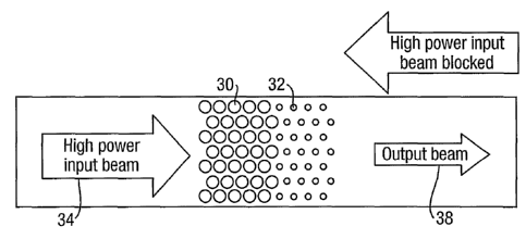
Referring to Figures 41 to 45, various further arrangements are
shown. Figure 41 is a diode structure based on the crystal lattice structure
shown
in Figure 40 in which a high power input beam approaching from the left-hand
side
provides at output beam, whereas a high power input beam from the right-hand
side is blocked. This is because the two regions of crystal lattice structure
30,32
provide two photonic band gaps with an upper edge of slightly different
values.
When a high power input beam is input from the left, the non linearity of the
lattice
structure 30 causes the band gap upper edge to be shifted downwardly in energy
so that the wavelength of the input beam is above the upper edge. Light is
therefore transmitted above both upper edges to provide an output beam.
However
light approaching from the right will influence the lattice structure 32 to
lower the
upper edge of the photonic band gap, but the photonic band gap in region 30
will
remain unchanged. Thus light will be blocked.
Referring to Figure 42 this shows a similar structure to that of
Figure 44, but wherein a high power bias optical signal 34 is provided, at any
desired wavelength in order to influence the structure 30 to lower the
photonic band
gap whereby to permit an input low power signal 36 having a signal wavelength
to
pass through the structure to provide an output beam 38. This structure
provides a
relay or switch function.
Referring to Figure 43, this shows a concrete implementation of the
concept shown in Figure 42 wherein the low power signal 36 and a high power
bias
signal 34 are conducted to the structure 30,32 by optical fibre paths 40,42.
Referring to Figure 44, this shows a schematic transistor arrangement
employing the structure 30,32 of Figure 41. A high power biasing beam 50 is
applied to region 30 to modulate the photonic band gap of region 30 whereby to
permit a fraction of an input light beam 36 to be transmitted as an output
beam 38.
Thus by careful adjustment of the parameters of power and signal wavelength,
the
power beam 50 acts to modulate the power to the output beam 38, in a manner
similar to a transistor.
CA 02404743 2010-11-15
20301-1917
In Figure 45, a lattice structure is employed 52 comprising a signal
region of a regular triangular lattice. A high power light beam 54 applied to
the
surface of the crystal structure modifies the photonic band gap to permit
light to be
propagated through the crystal structure as a beam 56.
The precise characteristics of a crystal structure with a similar form to
region 1 of Figure 40 had been determined experimentally as shown in
Figures 46 and 47.
Figure 46 shows propagation of TE and TM modes outside the band
gap, ie. with an energy greater than that of the upper level of the band gap,
but very
close to the upper band edge and Figure 47 shows propagation of both modes at
the energy level of the
30a
CA 02404743 2002-10-01
WO 01/77726 PCT/GBO1/01588
upper edge of the band gap.
In Figure 46 the inset at the lower left-hand side shows the signal wavelength
in
relation to the band gap, the signal wavelength being over 700nm whereas the
band
gap is in a region about 600nm. The main graphs compare spectra for a signal
laser
beam signal (which has passed through a photonic crystal structure embedded in
a
silicon nitride waveguide) with a reference laser beam (which has passed
through a
similar waveguide structure but which did not have a photonic crystal embedded
in
it), at two different power levels.
It may be seen that for both modes at wavelengths close to the upper band
edge,
1o there is little change in spectral properties for the reference laser beam
as the power
changes from low power (as shown in the lower graphs) to high power (as shown
in
the upper graphs).
However there is a significant change in spectral shape for light transmitted
through the signal beam which has passed through the photonic crystal as the
power
changes from low power to high power.
In comparison with the reference signal, the spectral shape of the laser beam
has
been flattened and shifted to slightly longer wavelengths.
This effect is due to an enhanced optical power density due to localisation
close
to the upper band edge. The increased optical power density has in turn caused
the
effective refractive index of the silicon nitride material to change slightly
due to an
induced non-linearity. This in turn has caused the edge of the band gap to
shift in
position.
Referring now to Figure 47, the graphs show the power dependent behaviour of
a photonic crystal device at shorter wavelengths lying just within the
photonic band
gap. The signal wavelength in relation to the band gap as shown in the inset
at the
upper left-hand side is of a value about 610nm.
It may be seen for the TE mode, the spectra for the beam transmitted through
the
photonic crystal is roughly the same as the reference spectra for both high
and low
power, although there is a small shift to longer wavelengths for the signal
beam.
For the TM mode, at both low and high power there is a considerable difference
between the reference and transmitted signal spectra.
31
CA 02404743 2002-10-01
WO 01/77726 PCT/GBO1/01588
In both cases, the signal transmitted through the photonic crystal has been
shifted considerably towards longer wavelengths. At low power (shown in the
lower
right-hand graph), the transmitted signal has a peak centered at about 620nm.
For a
high power input signal the transmitted signal has a wavelength spectra
centered
about 627nm. thus a power dependent wavelength change has been induced upon
the
signal by the influence of the photonic band gap.
This is caused by a shifting in the photonic band gap edge for high powers,
going to a slightly higher wavelength (lower energy). This edge shifting is
caused by
the non-linearity of the lattice structure. It should be noted that silicon
nitride which
the material is formed is not in itself a non-linear material but that the
triangular
lattice structure induces a strong linear non-linearity effect. For the
purposes of this
specification, non-linearity means that the refractive index of the material
is
dependent on the applied power of the optical signal.
32