Note: Descriptions are shown in the official language in which they were submitted.
CA 02405045 2002-10-03
WO 01/78192 PCT/CA01/00416
ELECTRICALLY CONNECTED MULTI-FEED ANTENNA SYSTEM
Field of the Invention
The present invention relates to antennas that can send and receive signals
from radio frequency (RF) communication devices. In particular the present
invention
relates to antennas that are used in portable hand held communication devices.
Background of the Invention
An antenna is a transforming element that converts circuit currents into
electromagnetic energy. Conversely, an antenna can also convert
electromagnetic
energy into circuit currents. The frequency to which an antenna responds is
based on
physical characteristics of the antenna such as width and length. Changes in
the width
and length of the antenna affect the resistance of the antenna and shape the
current
densities along the length of the antenna. The antenna field can be affected
by nearby
objects, such as other antennas, which distort the performance of the antenna.
In order to provide for operation of a communication device at different
frequencies, previous designs have included multiple distinct antennas, one
for each
desired operating frequency. Due to interference between the antennas and the
resultant inefficiencies however, multiple antenna arrangements may not be
feasible
in many applications, particularly in mobile communication devices with
limited
power supplies.
An alternative to such multiple antenna arrangements is a multiple feed
antenna. Known multiple feed antennas provide different antenna feeding ports
on the
CA 02405045 2002-10-03
WO 01/78192 PCT/CA01/00416
same type of antenna. Although the multiple ports allow for different antenna
element
lengths and thus different frequencies of operation, since the ports are
directly
connected to the same antenna, each port causes signal losses and other
interference
effects on antenna currents. For example, a transmission signal applied to the
antenna
by one feeding port will partially leak back through the antenna to the other
feeding
port instead of being converted into electromagnetic energy by the antenna,
thereby
reducing the efficiency of the antenna. Another major shortcoming of such
designs is
the coupling between antenna elements. The antenna type "seen" from both
feeding
:~::
points is the same, a monopole antenna in many conventional designs, resulting
a very
tight coupling between the antenna elements. This tight coupling may cause
serious
problems when the antenna system is implemented in a complicated environment.
For
example, changing the match for one of the feeding points is likely affect the
match of
the other one.
Thus, there remains a need for a portable hand-held communications device
that efficiently implements an antenna in at least a transmitting or a
receiving
configuration. There remains a further need for such an antenna system where
there is
some degree of isolation between the transmitting and receiving structures.
The
antenna preferably conforms to the housing of the device and is positioned so
that the
antenna will transmit and receive regardless of the orientation of the device
relative to
a communications station.
2
CA 02405045 2002-10-03
WO 01/78192 PCT/CA01/00416
Summary of the Invention
An antenna system for a portable transceiver device comprises an antenna
structure for transmitting and receiving RF signals. The antenna structure
includes
multiple feeding ports having a common structure fully coupling multiple
antennas of
different types to each other. This antenna structure is made of a conductor
that may
be surface mounted over a nonplanar surface, but may also be implemented as a
free-
standing element. When the conductor is mounted on a nonplanar surface, the
antenna structure preferably extends in three-dimensional space around a
portable
hand held communications device.
According to an embodiment of the invention, an antenna system comprises
an antenna structure, a first feeding port, and a second feeding port. The
first and
second feeding ports connect the antenna structure to communications
circuitry. The
antenna structure forms a first antenna structure of a first antenna type
connected to
the first feeding port and further forms a second antenna structure of a
second antenna
type connected to the second feeding port. Importantly, a portion of the first
antenna
structure is also a portion of the second antenna structure.
In a further embodiment of the present invention, there is also provided a
portable communications device comprising: a transmitting circuit; a receiving
circuit; and an antenna system, wherein the antenna system comprising a first
antenna
structure of a first antenna type and a second antenna structure of a second
antenna
type has a common portion of a radiation element fully coupling the first
antenna
structure to the second antenna structure. Preferably, the first antenna
structure and
the second antenna structure include a monopole antenna, a dipole antenna, and
a top
3
CA 02405045 2002-10-03
WO 01/78192 PCT/CA01/00416
loaded member wherein the top loaded member is . a portion of the first
antenna
structure and the second antenna structure. Preferred applications of the
present
invention include portable communication devices, wireless personal digital
assistants
(PDAs), two-way paging devices and cellular telephones.
Some of the advantages provided by the present invention include: high
efficiency, high gain, wide bandwidth, and low SAR. Furthermore, the use of
two
feeding points allows optimization of a communication module circuit board
layout to
minimize electromagnetic interference (EMI) problems. Since the antenna
structures
are electrically coupled, there are no performance issues regarding
electromagnetic
coupling between antennas in the present invention as in traditional separate
two-
antenna solutions wherein the electromagnetic coupling between the antennas
degrades the antenna performance.
Another advantage of the present invention is the simple layout, which
simplifies fabrication and thus provides for lower manufacturing costs. In
addition,
the present invention allows for the use of one piece of wire to realize two
different
antenna functions. A folded dipole used as a transmitting antenna in
accordance with
an aspect of the invention raises the antenna radiation resistance and thereby
increases
radiation efficiency.
Traditional dipoles and monopoles that are widely used in wireless devices
are very sensitive to a change in the environment. In contrast, the present
invention is
less sensitive to the environment. This can be accomplished according to an
aspect of,
the invention by introducing a balanced structure such as a dipole instead of
using two
4
CA 02405045 2002-10-03
WO 01/78192 PCT/CA01/00416
unbalanced structures such as monopoles for example. The balanced structure
will be
more immune from its the operating environment.
Brief Description of the Drawings
Further advantages and features of the invention will become apparent from
the following description, in which:
Fig. 1 is a top view of an antenna system comprising a preferred embodiment
of the invention;
Fig. 2 is an orthogonal view of the antenna system of Fig. 1 mounted on a
telecommunications device housing;
Fig. 3 is a partial view of the antenna system of Fig. 1;
Fig. 4 also is a partial view of the antenna system of Fig. 1; and
Fig. 5 is a block diagram of a communication device in which an antenna
system according to the invention may be implemented.
Description of a Preferred Embodiment
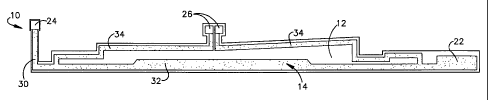
An antenna system 10 comprising a preferred embodiment of the present
invention is shown in Figure 1. The antenna system 10 comprises at least an
antenna
structure 14, which may be afl-ixed to a backing element 12. The backing
element 12
is preferably made of a thin, flexible material which merely provides
additional
physical, support for the antenna structure 14. Preferably, the antenna
structure 14 is
made of a low resistance conductor and affixed to the backing element 12. In
this
5
CA 02405045 2002-10-03
WO 01/78192 PCT/CA01/00416
manner, the antenna system 10 may be a laminate with layers of the antenna
structure
14 and the backing element 12.
The laminate arrangement shown in Fig. 1 provides increased structural
integrity of the antenna system 10. The backing element 12 performs no
operational
functions and the antenna structure 14 is fully operational without the
backing
element 12. Where the antenna system 14 is to be mounted on a further
structural
element and fabricated at the same time as the further element, the antenna
structure
may be mounted directly on the further structural element such that the
backing
element 12 is not necessary. If the antenna is separately fabricated and is to
be added
to a device after or during its manufacture however, the backing element is
preferred
in order to provide for handling of the antenna structure 14 while reducing
the
likelihood of damage thereto during such handling.
The antenna structure 14 has distinct portions defining a radiating element, a
top loading member 22, a monopole feeding port 24, and a dipole feeding port
26.
The radiating element is a conductor that extends from the feeding ports 24
and 26 to
the top loading member 22. Portions of the radiating element include: a
monopole
portion 30, a common portion 32, and a dipole portion 34. These portions 30-34
are
configured so that the radiating member includes a first antenna structure 40
(as
shown in Fig 3) that functions as an effective monopole antenna and a second
antenna
structure 44 (as shown in Fig 4) that functions as an effective dipole
antenna.
When the antenna system 10 is excited from the monopole feeding port 24, the
dipole feeding port 26 and the dipole portion 34 of the antenna structure 14
are a load
on the elective monopole antenna 40 (indicated as XX and YY on Fig. 3). When
the
6
CA 02405045 2002-10-03
WO 01/78192 PCT/CA01/00416
system is excited from the dipole feeding port 26, the monopole feeding port
24 and
the monopole portion 30 of the antenna structure 14 are a load on the
effective dipole
antenna 44 (indicated as ZZ on Fig. 4).
The effective monopole antenna 40 includes a current path along the radiating
element between the monopole feeding port 24 and the top loading member 22. As
shown in Fig. 3, the primary path of the effective monopole antenna 40 is
defined by
the monopole portion 30, the common portion 32 and the top loading member 22.
The
loads XX and YY between the monopole feeding port 24 and the top loading
member
22 have a high impedance due to the characteristic high input impedance of the
dipole
antenna 44, and consequently, very small amounts of current are delivered
through the
loads. The effective dipole antenna 44 includes a current path along the
radiating
element between the dipole feeding port 26 and the top loading member 22. As
shown
in Fig. 4, the path of the effective dipole antenna 44 comprises the dipole
portion 30,
the common portion 32, and the top loading portion 36. The load ZZ between the
dipole feeding port 26 and the top loading member 22 has a high impedance, and
consequently, a very small amount of current is delivered through the load.
Figure 2 shows a contemplated implementation of an antenna system
according to the above embodiment of the invention. A dielectric housing 46 is
a box-
shaped container made of a dielectric material. The dielectric housing 46 has
a top
and bottom surface 52 and 54, a front and back surface 56 and 58, and opposite
side
surfaces 60 and 62. Within the dielectric housing 46 is a transmitting circuit
70 and a
receiving circuit 74. The dielectric housing 46 holds the electronics of the
transmitting
circuit 70 and the receiving circuit 74.
7
CA 02405045 2002-10-03
WO 01/78192 PCT/CA01/00416
The antenna system 10 is folded 'from the original, flat configuration of Fig.
1
to the configuration in which it is mounted on the inside of the dielectric
housing 46,
as shown in Fig. 2. The antenna system 10 then extends around the dielectric
housing
46 to orient the antenna structure 14 in multiple perpendicular planes. The
top loading
member 22 and the common portion 32 of the radiating element are mounted on
the
side surface 60. The common portion 32 and the dipole portion 34 of the
radiating
element extend around a front corner 78 from the side surface 60 to the front
surface
56. The common portion 32 extends fully along the front surface 56 to the
opposite
corner 80. The dipole portion 34 turns upward from the front surface 56 to the
top
surface 52 and extends along the top surface 52. The dipole feeding port 26
also is
located on the top surface 52 of the dielectric housing 46. Near the corner
80, the
dipole portion 34 turns down from the top surface 52 back onto the front
surface 56.
The monopole portion 30 turns around the far front corner 80 from the front
surface
56 to the far side surface 62 and again turns from the side surface 62 upward
onto the
top surface 52. The effective monopole antenna 40 and the effective dipole
antenna 44
each extend in a plane parallel to the front surface 56, and planes parallel
to the top
surface 52, and the side surface 60. This orientation of the antenna system 10
makes
the portable communications device 56 an omnidirectional transmit and receive
device.
The monopole feeding port 24 is connected to the receiving circuit 74. The
dipole feeding port 26 is connected to the transmitting circuit 70.
Importantly, the
current distributed from the monopole feeding port 24 mainly flows along the
effective monopole antenna 40 while only a small amount of current travels
along the
8
CA 02405045 2002-10-03
WO 01/78192 PCT/CA01/00416
loads XX and YY. Since these loads are the high impedances of the dipole
portion
34, dipole feeding port 26 and transmitting circuitry 70, the current
distribution along
the effective monopole antenna 40 is minimally changed. Similarly, when
current is
distributed from the dipole feed port 26, the current mainly flows along the
effective
dipole antenna 44 while a small amount of current travels along the load ZZ.
Since the
load ZZ is the high impedance of the monopole portion 30, monopole feeding
port 24
and receiving circuit 74, the current distribution along the effective dipole
antenna 44
is minimally changed. This configuration is important in the operation of the
antenna
system 10 in its transmit and receive states.
The effective monopole antenna 40 is sized to receive signals from a radio
wave at a particular frequency by defining the length and width of its
radiating
element appropriately. Since the loads XX and YY have a high impedance, most
of
the current generated along the antenna structure 14 from the received radio
signal is
distributed along the effective monopole antenna 40. The length of the common
portion 32 of the radiating element is sized so that the antenna is tuned to
the chosen
frequency for receiving signals.
The effective dipole antenna 44 is sized to transmit a signal at a specified
frequency by defining the length and width of its radiating element
appropriately. The
high impedance of the load ZZ of the antenna structure 14 forces the current
from the
transmitting circuit 70 to flow along the effective dipole antenna 44. The
length of the
effective dipole antenna 44 is the length of both the common portion 32 and
the.
dipole portion 34. The dipole portion 34 can thus be sized with the prior
knowledge of
9
CA 02405045 2002-10-03
WO 01/78192 PCT/CA01/00416
the length of the common portion 32 to convert the circuit currents of the
transmitting
antenna to an electromagnetic signal at the desired frequency.
The top loading member 22 of the antenna structure 14 further alters the
current distribution of each effective antenna 40 and 44. The top loading
member thus
S further shapes the characteristics of each effective antenna 40 and 44 by
adding
perceived length to the antenna structure 14.
Fig. 5 is a block diagram of a mobile communication device 100 in which the
instant invention may be implemented. The mobile communication device 100 is
preferably a two-way communication device having at least voice and data
communication capabilities. The device preferably has the capability to
communicate
with other computer systems on the Internet. Depending on the functionality
provided
by the device, the device may be referred to as a data messaging device, a two-
way
pager, a cellular telephone with data messaging capabilities, a wireless
Internet
appliance or a data communication device (with or without telephony
capabilities).
Where the device 100 is enabled for two-way communications, the device will
incorporate a communication subsystem 110, including a transmitter 70 and a
receiver
74, as also shown in Fig. 2, an antenna system 10 incorporating antenna
elements 40
and 44, local oscillators (LOs) 112, and a processing module such as a digital
signal
processor (DSP) 114. Although separate antenna elements 40 and 44 are shown in
Fig. 5, it is to be understood that such antenna elements are electrically
connected as
described above to form an antenna system according to the invention. In the
embodiment shown in Fig. 2 for example, the antenna 10 could be mounted
directly
on a dielectric housing which encloses components of the communication device
100.
l0
CA 02405045 2002-10-03
WO 01/78192 PCT/CA01/00416
As will be apparent to those skilled in the field of communications, the
particular design of the communication subsystem 110 will be dependent upon
the
communication network in which the device is intended to operate. For example,
a
device 100 destined for a North American market may include a communication
subsystem 110 designed to operate within the MobitexTM mobile communication
system or DataTAC~ mobile communication system, whereas a device 101 intended
for use in Europe may incorporate a General Packet Radio Service (GPRS)
communication subsystem 110.
Network access requirements will also vary depending upon the type of
network 116. For example, in the Mobitex and DataTAC networks, mobile devices
such as 100 are registered on the network using a unique personal
identification
number or PIN associated with each device. In GPRS networks however, network
access is associated with a subscriber or user of a device 100. A GPRS device
therefore requires a subscriber identity module (not shown), commonly referred
to as
a SIM card, in order to operate on a GPRS network. Without a SIM card, a GPRS
device will not be fully functional. Local or non-network communication
functions (if
any) may be operable, but the device 100 will be unable to carry out any
functions
involving communications over network 116. When required network registration
or
activation procedures have been completed, a device 100 may send and receive
communication signals over the network 116.
Signals received by the antenna element 40 through a communication network
116 are input to the receiver 74, which may perform such common receiver
functions
as signal amplification, frequency down conversion, filtering, channel
selection and
11
CA 02405045 2002-10-03
WO 01/78192 PCT/CA01/00416
the like, and in the example system shown in Fig. 5, analog to digital
conversion.
Analog to digital conversion of a received signal allows more complex
communication functions such as demodulation and decoding to be performed in
the
DSP 114. In a similar manner, signals to be transmitted are processed,
including
S modulation and encoding for example, by the DSP 114 and input to the
transmitter 70
for digital to analog conversion, frequency up conversion, filtering,
amplification and
transmission over the communication network 116 via the antenna element 44.
The DSP 114 not only processes communication signals, but also provides for
receiver and transmitter control. For example, the gains applied to
communication
signals in the receiver 74 and transmitter 70 may be adaptively controlled
through
automatic gain control algorithms implemented in the DSP 114.
The device 100 preferably includes a microprocessor 118 which controls the
overall operation of the device. Communication functions, including at least
data and
voice communications, are performed through the communication subsystem 110.
The microprocessor 118 also interacts with further device subsystems such as
the
display 120, flash memory 122, random access memory (RAM) 124, auxiliary
input/output (I/O) subsystems 126, serial port 128, keyboard 130, speaker 132,
microphone 134, a short-range communications subsystem 136 and any other
device
subsystems generally designated as 138.
Some of the subsystems shown in Fig. 5 perform communication-related
functions, whereas other subsystems may provide "resident" or on-device
functions.
Notably, some subsystems, such as keyboard 130 and display 120 for example,
may
be used for both communication-related functions, such as entering a text
message for
12
CA 02405045 2002-10-03
WO 01/78192 PCT/CA01/00416
transmission over a communication network, and device-resident functions such
as a
calculator or task list.
Operating system software used by the microprocessor 118 is preferably
stored in a persistent store such as flash memory 122, which may instead be a
read
S only memory (ROM) or similar storage element (not shown). Those skilled in
the art
will appreciate that the operating system, specific device applications, or
parts thereof,
may be temporarily loaded into a volatile store such as RAM 124. It is
contemplated
that received communication signals may also be stored to RAM 124.
The microprocessor 118, in addition to its operating system functions,
preferably enables execution of software applications on the device. A
predetermined
set of applications which control basic device operations, including at least
data and
voice communication applications for example, will normally be installed on
the
device 100 during manufacture. Further applications may also be loaded onto
the
device 100 through the network 116, an auxiliary I/O subsystem 126, serial
port 128,
short-range communications subsystem 136 or any other suitable subsystem 138,
and
installed by a user in the RAM 124 or preferably a non-volatile store (not
shown) for
execution by the microprocessor 118. Such flexibility in application
installation
increases the functionality of the device and may provide enhanced on-device
functions, communication-related functions, or both. For example, secure
communication applications may enable electronic commerce functions and other
such financial transactions to be performed using the device 100.
In a data communication mode, a received signal such as a text message or
web page download will be processed by the communication subsystem 110 and
input
13
CA 02405045 2002-10-03
WO 01/78192 PCT/CA01/00416
to the microprocessor 118, which will preferably further process the received
signal
for output to the display 120, or alternatively to an auxiliary I/O device
126. A user of
device 100 may also compose data items such as email messages for example,
using
the keyboard 130, which is preferably a complete alphanumeric keyboard or
telephone-type keypad, in conjunction with the display 120 and possibly an
auxiliary
I/O device 126. Such composed items may then be transmitted over a
communication
network through the communication subsystem 110.
For voice communications, overall operation of the device 100 is substantially
similar, except that received signals would preferably be output to a speaker
132 and
signals for transmission would be generated by a microphone 134. Alternative
voice
or audio I/O subsystems such as a voice message recording subsystem may also
be
implemented on the device 100. Although voice or audio signal output is
preferably
accomplished primarily through the speaker 132, the display 120 may also be
used to
provide an indication of the identity of a calling party, the duration of a
voice call, or
other voice call related information for example.
The serial port 128 in Fig. 1 would normally be implemented in a personal
digital assistant (PDA)-type communication device for which synchronization
with a
user's desktop computer. (not shown) may be desirable, but is an optional
device
component. Such a port 128 would enable a user to set preferences through an
external device or software application and would extend the capabilities of
the device
by providing for information or software downloads to the device 100 other
than.
through a wireless communication network. The alternate download path may for
14
CA 02405045 2002-10-03
WO 01/78192 PCT/CA01/00416
example be used to load an encryption key onto the device through a direct and
thus
reliable and trusted connection to thereby enable secure device communication.
A short-range communications subsystem 138 is a further optional component
which may provide for communication between the device 100 and different
systems
or devices, which need not necessarily be similar devices. For example, the
subsystem
138 may include an infrared device and associated circuits and components or a
BluetoothTM communication module to provide for communication with similarly-
enabled systems and devices.
The invention has been described with reference to a preferred embodiment.
Those skilled in the art will perceive improvements, changes, and
modifications. Such
improvements, changes, and modifications are intended to be within the scope
of the
claims.
For example, other types of antennas will be apparent to those skilled in the
art. The invention is in no way limited to a mufti-feed antenna having a
monopole
antenna structure and a dipole antenna structure. Other types of antenna
structures
sharing a common antenna portion are also contemplated. Further types and
designs
of communication devices other than the device shown in Fig. 5 will also be
apparent.