Note: Descriptions are shown in the official language in which they were submitted.
CA 02405135 2002-09-25
01-H N M-364
METHOD AND APPARATUS FOR DETECTING AND SUPPRESSING A
PARALLEL ARC FAULT
Background of the Invention
[0001] The present invention relates to mechanisms that protect equipment
from damage due to electrical faults and short circuits; and particularly to
such
devices which electronically monitor performance of the electric equipment and
take
protective action in the event of a parallel arc fault.
[0002] It is important that electrical apparatus be protected from damage when
electrical failures occur. For example, conventional fuses and electro-
mechanical
circuit breakers are commonly employed to disconnect equipment from an
electrical
supply upon detection of excessive current when a short circuit occurs.
Nevertheless, these conventional protection devices are relatively slow in
disconnecting the current flow to the apparatus being protected. As a
consequence,
enough excessive electrical current can flow into the equipment to cause
damage
during a fault.
[0003] Furthermore, various electrical apparatus require different response
characteristics for the protection device. For example, electronic equipment
may
draw a substantially constant current level from initial start-up through a
normal shut-
down and be very intolerant of excessive current levels of even short
duration. The
protection device for such equipment has to respond very quickly to even
relatively
small over current conditions. Other types of electrical equipment draw large
instantaneous current levels at certain times, such as upon start-up, in
comparison to
the current level drawn during remainder of their operation. Thus, a circuit
protection
device that responds too rapidly to an high current condition may
inadvertently shut-
off current to the equipment during normally occurring events. As a
consequence,
the protection device for this type of equipment must respond in a manner that
tolerates brief high currents. The manner in which a protection device
responds to
over currents is referred to as the trip response characteristic or trip
curve, and has
to be matched to the particular type of electrical apparatus being protected.
[0004] This usually means that a manufacturer of protection devices must
design, manufacture and stock in inventory, a large variety of protection
devices that
have different trip response characteristics in terms of current level and
duration.
CA 02405135 2002-09-25
01-H N M-364
[0005] In the case of parallel arcs, it is difficult to detect a parallel arc
because
the arcs are often intermittent, unlike a bolted fault, or short circuit,
where the surge
of current is continuous.
[0006] Thus it is desirable to provide a protection device that can identify a
parallel arc fault. It is also desirable to provide a parallel arc protection
device that
can be customized easily with different trip response characteristics.
Summary of the Invention
[0007) An apparatus for protecting an electrical load from a parallel arc
fault
employs a semiconductor switch to connect the electrical load to a source of
current.
A current sensor is coupled in series with the semiconductor switch and
produces a
sensor signal that indicates the magnitude of current flowing to the
electrical load.
[0008] A control circuit is connected to the current sensor and the
semiconductor switch. The control circuit responds to the sensor signal by
producing a control signal that is applied to a control input of the
semiconductor
switch. In a first mode of operation when the magnitude of current is less
than a first
threshold, the control circuit maintains the semiconductor switch in a
continuous
conductive state. When the magnitude of current is greater than the first
threshold
and less than a second threshold, the control circuit in a second mode of
operation
renders the semiconductor switch non-conductive after a predefined period of
time.
In a third mode of operation when the magnitude of current is greater than the
second threshold, the semiconductor switch is alternately pulsed conductive
and
non-conductive by the control circuit to apply an average current through the
load
that is within an acceptable level wherein damage does not occur. When the
control
circuit pulses the semiconductor switch, the pulses are measured to determine
whether a parallel arc fault has occurred. When the measured pulses are within
a
predetermined range, a parallel arc fault is declared and the control circuit
renders
the semiconductor switch non-conductive.
Brief Description of the Drawings
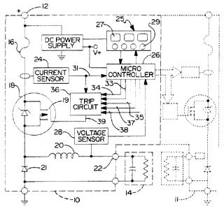
[0009] FIGURE 1 is a block diagram of a solid state circuit protector
according
to the present invention;
[0010] FIGURE 2 illustrates the details of an instant trip circuit in the
protector;
2
CA 02405135 2002-09-25
01-HNM-364
[0011] FIGURE 3 is a graph of an exemplary trip response characteristic of
the solid state circuit protector; and
[0012] Figure 4 is a diagram of exemplary pulses generated by the control
circuit measured within time windows according to the present invention.
Detailed Description of the Invention
[0013] With initial reference to Figure 1, a solid state circuit protector 10
controls application of a direct current to an electrical load 14, depicted as
capacitance in parallel with a resistance. The solid state circuit protector
10 has a
positive voltage terminal 12 which is connected to the electrical source for
powering
a load 14. Current flows from the positive voltage terminal to the load
through a
back-up fuse 16, a semiconductor switch 18 and an inductor 20 to a load
terminal
22. The load is connected between the load terminal 22 and the negative side
of the
voltage supply, represented as ground.
[0014] The back-up fuse 16 is a conventional device with a conductor which
heats-up and ultimately breaks when excessive current flows for a given period
of
time. Standard devices, such as glass tube encased fuses or an appropriate
trace
on printed circuit board, can be employed for the back-up fuse 16. The back-up
fuse 16 provides redundant protection in case the semiconductor switch 18
fails in
the conductive state or upon failure of electronic circuits controlling the
semiconductor switch. As will be understood, the trip response time of the
back-up
fuse is considerably slower than the trip response characteristic of the
electronic
circuit protection.
[0015] The semiconductor switch 18 must be able to interrupt the load current
and handle transient currents, over currents and in-rush at a specified
operational
voltage range as dictated by the particular load 14 to be controlled. An n-
channel
field effect transistor (FET), such as model IRF1404 from International
Rectifier of EI
Segundo, CA 90245 USA may be used as the semiconductor switch 18. The
channel resistance in the conductive state has to be relatively low to
minimize the
voltage drop across the FET and the heat dissipation. Although the preferred
embodiment employs the semiconductor switch 18 between the positive voltage
terminal 12 and the load 14, alternatively the switch could be placed on the
ground
3
CA 02405135 2002-09-25
01-HNM-364
side of the load. However, this alternative approach has the disadvantage that
a
fault from load to ground would be unprotected.
[0016] A voltage sensor 28 produces an analog signal which indicates the
voltage level at the load terminal. That analog signal is applied to an analog
input of
a microcontroller 26. As will be described, the microcontroller 26 responds to
an
indication from the sensor 28 that the voltage across the load 14 is too low
by turning
off the semiconductor switch 18.
[0017] A current sensor 24 is provided to detect the level of current flowing
between the positive voltage terminal 12 and the load 14. This sensor must
have a
dynamic range which is large enough to cover the current extremes for the
desired
trip response characteristic of the protection device and have a transient
response
that is sufficiently fast to implement the desired trip response
characteristic. The
current sensor 24 may be a Hall effect sensor that produces an output voltage
indicative of the DC current magnitude and which output voltage can be applied
via
line 31 directly to an analog input of a microcontroller 26. Other types of
conventional current sensors, such as a shunt resistor, may be used to provide
a
current magnitude indication to the microcontroller 26.
[0018] The microcontroller 26 is microprocessor based and includes an
internal analog-to-digital converter with a multiplexed input for signals from
the
current and voltage sensors. Digital input/output circuits of the
microcontroller handle
signals for other components of the solid state circuit protector 10. For
example, a
user control panel 25 has a keypad 27 and light emitters 29, such as LED's.
The
keypad 27 has separate momentary contact switches that supply input signals to
the
microcontroller 26 to manually turn the solid state circuit protector 10 on
and off, as
well as reset a trip condition. The light emitters 29 are powered by signals
from the
microcontroller to indicate the operational states of the circuit protector.
One of
those light emitters 29 indicates when the circuit protector 10 is tripped.
The
microcontroller 26 also has an internal non-volatile memory which stores a
software
program defining the protection function and which stores data, such as the
trip
response characteristic, for use by that software program. The microcontroller
26
and the control panel 25 optionally can control additional poles of a circuit
protector
as indicated by a second pole 11 drawn in phantom lines.
4
CA 02405135 2002-09-25
01-HNM-364
[0019] The microcontroller 26 operates the semiconductor switch 18 through a
trip circuit 36 that generates a drive voltage which is adequate to control
the FET 19
in the preferred embodiment of the semiconductor switch 18. Because the
voltage
driving the gate of an N-channel FET 19 has to be approximately ten volts
greater
than the voltage at the source electrode of the FET, the trip circuit 36
includes a
charge pump or similar circuit to generate voltage greater than that found on
the
positive input terminal 12.
[0020] Figure 2 illustrates the details of the trip circuit 36 wherein the
output
signal IsENSE on line 31 from the current sensor 24 is applied to a first
voltage
comparator 40. The sensed current level IsENSE is compared to a second
threshold
ITHZ which is produced on an analog output line 37 of the microcontroller 26.
A fixed
value for the second threshold ITH2 is programmed into the microcontroller 26
depending upon the over current tolerance of the specific load 14. The result
of that
comparison at the output of the first comparator 40 is applied to the RESET
input of
a flip-flop 42. The reset input also is connected to a positive supply voltage
V+ by a
pull-up resistor 44.
[0021] The SET input of the flip-flop 42 is connected to the output of a dual
input NAND gate 46, having both inputs tied together to function as an
inverter. The
inputs of first NAND gate 46 are connected to a digital output line 33 from
the
microcontroller 26 which carries a pulsed signal at a fixed frequency in
excess of 15
kHz., specifically in the range of 20-80 kHz. and preferably at 50 kHz. The
pulsed
signal has a fixed duty cycle thereby forming a train of constant-width
pulses. As will
be described, the pulse train periodically sets the flip-flop output which is
tied to one
input of a second NAND gate 48 having three inputs. Another input of the
second
NAND gate 48 receives an ON signal on another digital output line 33 from the
microcontroller 26. Whether the ON signal is active or inactive is determined
by
manual operation of switches on keypad 27 of the control panel 25.
[0022] The third input of the second NAND gate 48 receives an output signal
from an instant trip mechanism formed by a second voltage comparator 50 and a
second flip-flop 51. Specifically, the second comparator 50 compares the
current
sensor output signal IsENSE to a third threshold ITH3. The third current
threshold ITH3 is
generated on another analog output line 38 by the microcontroller 26 and is
defined
by a fixed value programmed into the solid state protection circuit 10. The
third
5
CA 02405135 2002-09-25
01-H N M-364
current threshold ITH3 is greater than the second current threshold ITHZ. The
precise
relationship between those two current thresholds will become apparent from a
subsequent description of the operation of the solid state current protection
circuit.
The second and third current thresholds I-rH2 and ITH3, instead of being
programmable, may be set by conventional voltage dividers at the inputs to the
respective comparators 40 and 50. The output of the second comparator 50 is
latched by the second flip-flop 51 with an output connected to another input
of the
second NAND gate 48. The set input of the second comparator 50 is connected to
RESET output line 35 from the microcontroller 26.
[0023] The components of the trip circuit 36 described thus far, provide input
signals to the second NAND gate 48. The output of that gate is fed through a
third
NAND gate 52 which is connected as an inverter. The signal emanating from the
third NAND gate 52 is coupled by a resistor 56 to an isolation circuit 54,
such as a
standard opto-isolator. The isolation circuit 54 produces an output on line 58
that is
applied to an input of a conventional FET gate driver circuit 60. A charge
pump 62
provides a voltage level that the FET gate driver 60 uses to bias the gate of
the FET
19 via line 39.
[0024] The operation of the solid state circuit protector 10, in Figure 1,
commences with the operator pressing an appropriate switch on keypad 27. The
microcontroller 26 responds to this switch activation by applying a high
level, or
active ON signal, via line 34 to the second NAND gate 48. At this time, the
microcontroller 26 also begins producing a pulse train on digital output line
33
connected to the first NAND gate 46. A high logic level of that pulse train
causes the
output of the first flip-flop 42 to go high, applying another high level to
another input
of the second NAND gate 48.
[0025] During normal operation of the load 14, the output signal IsErvsE from
the current sensor 24 is less than the third threshold ITH3. As a consequence,
the
second voltage comparator 50 produces a high logic level at the third input of
the
second NAND gate 48. Thus the second NAND gate 48 produces a low level output
signal that, upon inversion by the third NAND gate 52 and conduction through
isolator 54, activates the FET gate driver 60. This causes the gate driver 60
to bias
the gate of the FET 19 into a conductive state, thereby applying current from
the
positive voltage terminal 12 through the inductor 20 to the load 14.
6
CA 02405135 2002-09-25
01-H N M-364
[0026] The level of current through the semiconductor switch 18 rises rapidly
and soon exceeds the second threshold ITH2. At that time, the output of the
first
comparator 40 goes low resetting the flip-flop 42 and causing the second NAND
gate
48 to change output states. This results in the FET gate driver 60 rendering
the
semiconductor switch 18 non-conductive. The energy stored in the inductor 20
produces a decaying current that flows through the load 14 and the fly back
diode
21.
[0027] When the next positive pulse occurs in the pulse train on line 33 to
the
first NAND gate 46, the flip-flop 42 will be SET to produce another high logic
output
level which once again turns on the FET gate driver 60 and the semiconductor
switch 18. This on-off cycling of the semiconductor switch continues chopping
the
current at the rate of the signal on line 33 until the capacitance in the load
14
adequately charges, at which time the load current becomes substantially
constant
at a level less than the second threshold ITHZ. Thus the load current during
start-up
is limited to being less than the second threshold ITH2 while still applying
current to
initialize the load operation. Once the excursions of current through the
semiconductor switch 18 fall below this threshold, the flip-flop 42 no longer
is reset
and the FET gate driver 60 maintains the semiconductor switch 18 in a
conductive
state. That conductive state continues as long as the load 14 functions
normally.
[0028] If there is a fault with the load during start-up, the load current
does not
drop below the second threshold ITH2. The current chopping could continue
indefinitely in this case. To prevent that, the duration of the current
chopping is
limited by counting the current pulses applied to the load and terminating the
chopping upon the occurrence of given number of pulses that normally is
sufficient to
charge a typical load capacitance. Specifically, the microcontroller 26
monitors the
input line 31 from the current sensor 24 which indicates alternate high
current and
zero current conditions and counts the number of high current pulses.
[0029] That count is compared to a reference number and the chopping mode
is terminated when that reference number of current pulses has occurred. At
that
time, the microcontroller 26 sends a low logic level signal on line 34 to the
trip circuit
36, which renders the semiconductor switch 18 non-conductive until a person
presses the RESET switch on the control panel 25 and resets the
microcontroller 26.
CA 02405135 2002-09-25
01-HNM-364
(0030] A parallel arc fault is more difficult to detect than a short circuit,
or
"bolted fault". A parallel arc fault may result from worn insulation on a
wire, as an
example, resulting in an intermittent short. The microcontroller 26 of the
circuit
protector 10 detects a parallel arc fault by measuring the pulses applied to
the load
14. The microcontroller 26 may measure the pulses by monitoring the input line
31
from the current sensor 24 or by monitoring the pulses sent to the FET gate
driver
60.
[0031] A number of algorithms may be applied to declare a parallel arc fault.
For example, a number of pulses within an infinite time period, a number of
pulses
within a predetermined time period, a number of periods with a declared
parallel arc
fault, when the number of pulses are within a predetermined range, or any
combination of the above. It should also be noted that "measured" when
referring to
the pulses may mean integrated, counted or any other mathematical operation.
It
should be understood that pulses sent to the FET gate driver 60 are a
representation
of the percentage of time that IsENSE is greater than ITH1. When the measured
pulses
meet a predetermined criteria, a parallel arc fault is declared and the
semiconductor
switch 18 is rendered non-conductive.
[0032] Alternatively the voltage sensor 28 can be employed to safeguard
against operating in the current chopping mode for too long a time period.
During a
short circuit condition when the load 14 is drawing excessive current, the
voltage
across the load will be significantly lower than during normal operation. The
voltage
across the load 14 is detected by the voltage sensor 28 which applies an
analog
voltage level indication to the microcontroller 26. If that sensed load
voltage remains
below a given threshold for greater than a predefined time interval during the
current
chopping mode, the microcontroller 26 turns off the trip circuit 36 by
applying a low
logic level, (an inactive ON signal) to the ON/OFF line 34.
[0033] The operation of the solid state protection circuit 10 during an over
current condition after a normal start-up may best be understood with respect
to an
exemplary trip response characteristic, such as the one depicted in Figure 3.
A load
current which is below a first threshold ITH~ can be tolerated indefinitely by
the load
14 and thus will be conducted continuously by the semiconductor switch 18. The
first threshold ITH~ is set between 100% and 125% of the current rating for
the load
14 being protected. Load currents between levels ITH~ and 12 can be tolerated
by the
s
CA 02405135 2002-09-25
01-HNM-364
load for an amount of time which is inversely proportional to the current
magnitude.
In other words, small deviations above the first threshold ITH~ can be
tolerated for a
longer period of time than over currents which approach level 12. This
produces a
linear trip response characteristic in portion 70 of the response curve. This
portion of
the trip response characteristic is programed into the microcontroller 26 and
stored in
its memory either as a linear equation or as a data table. That data table has
pairs
of values with one value being a current magnitude and the other value
defining a
time interval during which that current magnitude can be tolerated before the
solid
state circuit protector 10 must trip.
[0034] Current between level 12 and the third threshold ITHS can be tolerated
by the load for a period designated T1. Current above that higher level ITHS
cannot
be tolerated by the load 14, even momentarily, and thus the current protection
device
will trip immediately. It should be noted, that load current within the cross-
hatched
region 72 between second threshold ITHZ and a third threshold ITHS while
tolerated by
the load 14, can damage the FET 19. Thus, when operation within this region is
determined to occur, the solid state circuit protector 10 enters a current
chopping
mode of operation. In this mode the semiconductor switch is pulsed on and off
at a
rate which produces an average current that is less than the second threshold
ITH2.
Thus the load remains powered so that the load capacitance remains charged but
the current applied to the load is limited to that second threshold level.
[0035] When the sensed current IsENSE is between the first threshold ITH~ and
a second threshold ITH2, the trip circuit 36 initially maintains semiconductor
switch 18
in a conductive state because that current is below the two comparator
thresholds
ITH2 and ITH3. However, the microcontroller 26 receives the output signal
IsENSE from
the current sensor 24 on line 31 utilizes the programed trip response
characteristic
for section 70 to determine whether to turn-off the semiconductor switch 18.
Specifically, the microcontroller 26 determines whether the over current
magnitude
has occurred for the time period defined by the trip response characteristic.
Once
that has occurred, the microcontroller 26 turns off the trip circuit 36 by
applying a low
logic level, inactive ON signal, to the digital line 34. This constant low
logic level
toggles the output level from the second NAND gate 48 which turns-off the FET
gate
driver 60 and thus the semiconductor switch 18. The microcontroller 26 also
illuminates the light emitter 29 on the control panel 25 which indicates the
tripped
9
CA 02405135 2002-09-25
01-H N M-364
condition. The OFF signal continues to be applied by the microcontroller 26 to
the
trip circuit 36 until a manual reset switch on the control panel 25 pressed.
[0036] When the sensed load current signal IsENSE is between the current
thresholds ITH2 and ITH3, the microcontroller 26 does not utilize the trip
response
characteristic data to determine whether to turn-off the trip circuit 36.
Instead, the
solid state protection circuit 10 enters a current chopping mode in which the
FET 19
is pulsed on and off at the rate of the pulsed signal on line 33.
[0037] Specifically with reference to Figure 2, when the current sensor 24
produces an output signal IsENSE on line 31 which is greater than the second
threshold ITH2 on line 37, the output of first comparator 40 goes low. That
low output
resets the flip-flop 42, thereby applying a low logic level to an input of the
second
NAND gate 48. This produces a high logic level at the output of the second
NAND
gate 52 which is inverted by the third NAND gate 52 thus applying a low logic
level to
the opto-isolator 54. This in turn deactivates the FET gate driver 60 which
renders
the semiconductor switch 18 nonconductive. At that time current from the
inductor
flows through the load 14 and a fly back diode 21.
[0038] The semiconductor switch 18 remains off until the next high logic level
pulse in the pulse train from the microcontroller 26 that is applied to the
trip circuit 36
on digital line 33. That pulse upon inversion by the first NAND gate 46 sets
the flip-
20 flop 42 which produces a high output level that is applied to the second
NAND gate
48. This high logic level activates the FET gate driver 60, once again
rendering the
semiconductor switch 18 conductive.
[0039] When the FET 19 turns on again, the inductor 20 limits the rate at
which the current rises so that the current level does not immediately exceed
the
second threshold ITH2. Thus, a small amount of current will be applied to the
load 14
and charging its capacitance. However, the current through the semiconductor
switch 18 eventually rises above the second current threshold ITHZ which will
be
detected by the first comparator 40. When this occurs the first comparator 40
changes output states and resets the flip-flop 42, which in turn applies a
signal to the
second NAND gate 48 that ultimately results in the FET gate driver 60 shutting
off
the semiconductor switch 18. This cycling of the semiconductor switch 18 off
and on
continues which results in an average load current that is below the first
threshold
ITH1
CA 02405135 2002-09-25
01-HNM-364
[0040] Although the semiconductor switch 18 is not exposed to as great a
degree of thermal stress as with linear current limiting, damage to the FET 19
or the
load still may occur if the current chopping mode continues for too long a
time
period. As discussed previously with respect the start-up operation of the
solid state
circuit protector 10, the duration of the current chopping can be limited by
the
microcontroller 26 counting the number of current pulses applied to the load
and
sending a low logic level OFF signal on line 34 to the trip circuit 36 when a
given
number of pulses has occurred. Alternatively the voltage sensor 28 can be
employed to detect a short circuit and inform the microcontroller 26 to turn-
off the trip
circuit 36.
[0041] The parallel arc fault detection logic may be best understood with
reference to an exemplary pulse signals detected by the microcontroller 26
depicted
in Figure 4. A series of pulses 74 is shown indicative of the number of
current pulses
applied to the load 14. A parallel arc fault may be declared when a number of
pulses
74 are detected by the microcontroller 26. Additionally, the microcontroller
26 may
count the number of pulses 74 over a period of time. Alternatively, a range
for
declaring a parallel arc fault may be programmed into the microcontroller 26
or be
hard coded into the logic.
[0042] In the preferred embodiment, the first pulse 74 initializes the
microcontroller. The pulse train has a frequency of 50 kHz, rendering a
maximum of
50 pulses per millisecond. It should be noted that the frequency range of the
pulse
train is application specific and should not be deemed to be limiting upon the
present
invention. Each pulse 74 causes an interrupt which increments a counter. The
counter decrements once every 100 milliseconds to reduce any nuisance trips.
The
count is analyzed every millisecond. The microcontroller 26 is set to declare
a bolt
fault if 36 or more pulses are counted within a 1 millisecond window. If the
microcontroller 26 counts between 1 pulse and 36 pulses in a 1 millisecond
window
a parallel arc fault is declared, sending a low logic level OFF signal on line
34 to the
trip circuit 36.
[0043] The microcontroller 26 may evaluate a series of windows. The results
of a previous number of windows will remain in the memory of the
microcontroller 26.
For example, when four of six previous 1 millisecond windows declare a
parallel arc
fault, the microcontroller 26 will declare a parallel arc fault and render the
11
CA 02405135 2002-09-25
01-H N M-364
semiconductor switch 18 non-conductive. The memory of the microcontroller 26
is
reset when no pulses are detected for 6 milliseconds. Those skilled in the art
will
recognized that the aforementioned time segments and numbers of pulses are for
exemplary purposes and should not be deemed to be limiting upon the scope of
the
present invention.
[0044] The current chopping should ensure that the load current never
exceeds the third threshold level ITHS. However, in the event that a
malfunction
occurs, the second comparator 50 detects a load current above that third
threshold
level IrH3 and produces an output that renders the semiconductor switch 18
continuously non-conductive. Specifically, the output of the second comparator
50
goes low which resets the second flip-flop 51 thereby applying a low logic
level to the
second NAND gate 48. This results in the FET turning off.
12