Note: Descriptions are shown in the official language in which they were submitted.
CA 02405267 2002-10-03
WO 01/77678 PCT/USO1/11320
TWO-DIMENSIONAL SPECTRAL IMAGING SYSTEM
CROSS-REFERENCES TO RELATED APPLICATIONS
The application claims the benefit of priority from co-pending U.S.
Provisional Patent Application No. 60/195,520 entitled "Method for Encoding
Materials with
Semiconductor Nanocrystals, Compositions Made Thereby, and Devices for
Detection and
Decoding Thereof," filed April 6, 2000, the full disclosure of which is
incorporated herein by
reference.
The subject matter of the present application is related to the following co-
pending patent applications, the disclosures of which are also incorporated
herein by
reference: U.S. Patent Application No. 09/160,458 filed September 24, 1998 and
entitled,
"Inventory Control"; U.S. Patent Application No. 09/397,432 filed September
17, 1999, and
also entitled "Inventory Control"; PCT Patent Application No. WO 99/50916 as
published on
April 1, 1999, entitled "Quantum Dot White and Colored Light Emitting Diodes";
and U.S.
Patent Application No. 09/259,982 filed March 1, 1999, and entitled
"Semiconductor
Nanocrystal Probes for Biological Applications and Process for Making and
Using Such
Probes".
BACKGROUND OF THE INVENTION
The present invention generally provides devices, compositions of matter,
bits,
systems and methods for detecting and identifying a plurality of signals from
within a signal
area. In a particular embodiment, the invention provides systems and methods
for detecting
and identifying a plurality of spectral barcodes from throughout a sensing
area, especially for
identifying andlor tracking inventories of elements, for high-throughput assay
systems, and
the like. The invention will often use labels which emit identifiable spectra
that include a
number of discreet signals having measurable wavelengths andlor intensities.
Tracking the locations and/or identities of a large number of items can be
challenging in many settings. Barcode technology in general, and the Universal
Product
Code in particular, has provided huge benefits for tracl~ing a variety of
objects. Barcode
technologies often use a linear array of elements printed either directly on
an object or on
labels which may be affixed to the object. These barcode elements often
comprise bars and
CA 02405267 2002-10-03
WO 01/77678 - PCT/USO1/11320
spaces, with the bars having varying widths to represent strings of binary
ones, and the spaces
between the bars having varying widths to represent strings of binary zeros.
Barcodes can be detected optically using devices such as scanning laser beams
or handheld wands. Similar barcode schemes can be implemented in magnetic
media. The
scanning systems often electro-optically decode the label to determine
multiple
alphanumerical characters that are intended to be descriptive of (or otherwise
identify) the
article or its character. These barcodes are often presented in digital form
as an input to a
data processing system, for example, for use in point-of-sale processing,
inventory control,
and the lilce.
Barcode techniques such as the Universal Product Code have gained wide
acceptance, and a variety of higher density alternatives have been proposed.
Unfortunately,
these standard barcodes are often unsuitable for labeling many "libraries" or
groupings of
elements. For example, small items such as jewelry or minute electrical
components may
lack sufficient surface area for convenient attachment of the barcode.
Similarly, emerging
technologies such as combinatorial chemistry, genomics research,
microfluidics,
micromachines, and other nanoscale technologies do not appear well-suited for
supporting
known, relatively large-scale barcode labels. In these and other developing
fields, it is often
desirable to make use of large numbers of fluids, and identifying and tracking
the movements
of such fluids using existing barcodes is particularly problematic. While a
few chemical
encoding systems for chemicals and fluids have been proposed, reliable and
accurate labeling
of large numbers of small and/or fluid elements remains a challenge.
Small scale and fluid labeling capabilities have recently advanced radically
with the suggested application of semiconductor nanocrystals (also known as
Quantum DotTM
particles), as detailed in U.S. Patent Application No. 09/397,432, the full
disclosure of which
is incorporated herein by reference. Semiconductor nanocrystals are
microscopic particles
having size-dependent optical and/or electrical properties. As the band gap
energy of such
semiconductor nanocrystals vary with a size, coating and/or material of the
crystal,
populations of these crystals can be produced having a variety of spectral
emission
characteristics. Furthermore, the intensity of the emission of a particular
wavelength can be
varied, thereby enabling the use of a variety of encoding schemes. A spectral
label defined
by a combination of semiconductor nanocrystals having differing emission
signals can be
identified from the characteristics of the spectrum emitted by the label when
the
semiconductor nanocrystals are energized.
2
CA 02405267 2002-10-03
WO 01/77678 - PCT/USO1/11320
While semiconductor nanocrystal-based spectral labeling schemes represent a
significant advancement for tracking and identifying many elements of
interest, still further
improvements would be desirable. In general, it would be beneficial to provide
improved
techniques for sensing or reading these new spectral labels. It would be
particularly
beneficial to provide improved techniques for applying these labeling and
tracking
technologies to high-throughput assay systems now being developed.
Multiplexed assay formats would be highly desirable for improved throughput
capability, and to match the demands that combinatorial chemistry is putting
on established
discovery and validation systems for pharmaceuticals. For example,
simultaneous
elucidation of complex protein patterns may allow detection of rare events or
conditions, such
as cancer. In addition, the ever-expanding repertoire of genomic information
would benefit
from very efficient, parallel and inexpensive assay formats. Desirable
multiplexed assay
characteristics include ease of use, reliability of results, a high-throughput
format, and
extremely fast and inexpensive assay development and execution.
A number of known assay formats may be employed for high-throughput
testing. Each of these formats has limitations, however. By far the most
dominant high-
throughput technique is based on the separation of different assays into
different regions of
space. The 96-well plate format is the workhorse in this arena.
In 96-well plate assays, the individual wells (which are isolated from each
other by walls) are often charged with different components, and the assay is
performed and
then the assay result in each well measured. The information about which assay
is being run
is carried with the well number, or the position on the plate, and the result
at the given
position determines which assays are positive. These assays can be based on
chemiluminescence, scintillation , fluorescence, scattering, or
absorbance/colorimetric
measurements, and the details of the detection scheme depend on the reaction
being assayed.
Mufti-well assays have been reduced in size to enhance throughput, for
example, to accommodate 384 or 1536 wells per plate. Unfortunately, the fluid
delivery and
evaporation of the assay solution at this scale are significantly more
confounding to the
assays. High-throughput formats based on mufti-well arraying often rely on
complex
robotics and fluid dispensing systems to function optimally. The dispensing of
the
appropriate solutions to the appropriate bins on the plate poses a challenge
from both an
efficiency and a contamination standpoint, and pains must be talcen to
optimize the fluidics
for both properties. Furthermore, the throughput is ultimately limited by the
number of wells
that one can put adjacent on a plate, and the volume of each well. Arbitrarily
small wells
CA 02405267 2002-10-03
WO 01/77678 - PCT/USO1/11320
have arbitrarily small volumes, resulting in a signal that scales with the
volume, shrinking
proportionally with the cube of the radius. The spatial isolation of each
well, and thereby
each assay, has been much more common than running multiple assays in a single
well. Such
single-well multiplexing techniques are not widely used, due in large part to
the difficulty in
"demultiplexing" or resolving the results of the different assays in a single
well.
For even higher throughput genomic and genetic analysis techniques,
positional array technology has been shrunk to microscopic scales, often using
high-density
oligonucleotide arrays. Over a 1-cm square of glass, tens to hundreds of
thousands of
different nucleotides can be written in, for example, 25-~,m spots, which are
well resolved
from each other. On this planar test structure or "chip," which is emblazoned
with an
alignment grid, a particular spot's x,y position determines which
oligonucleotide is present at
that spot. Typically fluorescently-labeled amplified DNA is added to the
array, hybridized
and is then detected using fluorescence-based techniques. Although this is a
very powerful
technique for assaying a large number of genetic markers simultaneously, the
cost is still very
high, and the flexibility of this assay is extremely limited.
Once a chip is made with particular DNA sequences at particular locations,
they are fixed and the addition thereto of new markers comes at a very high
price. The
extremely small feature size, and the highly parallel assay format, comes at
the cost of the
flexibility inherent in a common platform system, such as the 96-well plates.
In addition, this
assay is ultimately performed at the surface of the chip, and the results
depend on the
kinetics of the hybridization to the surface, a process that is negatively
influenced by steric
issues, mixing issues, and diffusion issues. In fact, small microarray chips
are not
particularly suited to the detection of rare events, as the diffusion of the
solution over the chip
may not be sufficiently thorough. In order to perform the hybridizations to
the microarray
chips more efficiently, a dedicated fluidics workstation can be used to pump
the solution over
the surface of the chip repeatedly; such instruments add cost and time to
execution of the
assay.
The use of spectral barcodes holds great promise for enhancing the throughput
of assays, as described in an application entitled "Semiconductor Nanocrystal
Probes for
Biological Applications and Process for Making and Using such Probes," U.S.
Application
No. 09/259,982 filed March 1, 1999, the full disclosure of which is
incorporated herein by
reference. Multiplexed assays may be performed using a number of probes which
include
both a spectral label (often in the form of several semiconductor
nanocrystals) and one or
more moieties. The moieties may be capable of selectively bonding to one or
more
4
CA 02405267 2002-10-03
WO 01/77678 PCT/USO1/11320
detectable substances within a sample fluid, while the spectral labels can be
used to identify
the probe within the fluid (and hence the associated moiety). As the
individual probes can be
quite small, and as the number of barcodes which can be independently
identified can be
quite large, large numbers of individual assays might be performed within a
single fluid
sample by including a large number of differing probes. These probes may take
the form of
quite small beads, with each bead optionally including a spectral label, a
moiety, and a bead
body or matrix, often in the form of a polymer.
Together with the substantial advantages provided by highly multiplexed,
spectrally-encoded assay bead systems, there will be significant challenges in
implementing
these techniques. In particular, determining multiplexed assay results might
be quite
challenging. While the reaction times and accuracy of the spectral labels can
be quite
advantageous, it can be challenging to accurately read each spectral barcode
and/or assay
result from the hundreds, and in many cases thousands, of beads within a
highly multiplexed
bead assay system. Similarly, while spectral coding in general allows labeling
and/or
identification of a large number of elements, interpreting the spectral codes
can be quite
challenging when the individual label structures are small, and when many
labels are located
near each other.
In light of the above, it would generally be desirable to provide improved
systems and methods for detecting and identifying signals. It would be
particularly beneficial
if these improved techniques facilitated the identification of each spectral
code from among a
plurality of spectral barcodes in a given region. To take advantage of the
potential
capabilities of spectral coding of minute probes and other structures, it
would be highly
desirable if these enhanced techniques allowed detection and/or identification
of large
numbers of spectral codes or other signals (such as assay marker signals) in a
highly time
efficient manner.
SUMMARY OF THE INVENTION
The present invention generally provides improved devices, systems, and
methods for sensing and/or identifying signals. The techniques of the present
invention are
particularly well-suited for identification of labels which generate spectral
codes. Large
numbers of independently identifiable spectral codes can be generated by quite
small bodies
having such labels, and a plurality of such bodies or probes may be present
within a detection
region. In some embodiments, the invention allows simultaneously imaging of
identifiable
5
CA 02405267 2002-10-03
WO 01/77678 PCT/USO1/11320
spectra from throughout the detection region. This simultaneous imaging allows
the labels
(and hence, the associated probes, assay results, and the like) to be
identified. A wavelength
dispersive element (for example, a prism, diffractive grating, holographic
transmissive
grating, or the like) can simultaneously spectrally disperse the images of the
labels across a
sensor surface. A two-dimensional areal light sensor (such as a Charge-Coupled
Device or
"CCD") can substantially simultaneously sense the relative wavelengths of
signals making up
the spectra. Taking advantage of a very small label size, the identifiable
spectra can be treated
as being generated from point-sources within a large detection field, thereby
acting as their
own "slit" in this spectroscopic instrument. Absolute signal wavelengths may
be identified
by determining positions of the labels, using an internal wavelength reference
within the
spectra, and/or the like.
Spectral labels may be used with other markers generating signals that differ
significantly from the identifiable spectra from the labels. For example,
spectrally encoded
beads may be used within parallel assay systems by generating assay signals in
addition to
the label spectra. These assay signals may accurately and reliably indicate
the results of the
assay, but these signals may be significantly lower in intensity than the
spectral label. Hence,
the present invention also provides techniques for identifying signals of
widely varying
strengths. These techniques often involve simultaneously sensing lower
intensity signals
using a relatively long integration time with areal imaging. Higher intensity
signals can be
sequentially sensed, often using a scanning system. This dual sensing system
enhances the
overall efficiency of signal detection and interpretation by allowing a
relatively long signal
integration time for the lower intensity signals, while the higher intensity
signals are quickly
scanned with a shorter integration time. In some embodiments, a plurality of
excitation
energies may be directed toward the signal generators, with at least one of
the excitation
2~ energies selectively producing the lower energy signals. Such techniques
are particularly
well-suited to take advantage of the capabilities of semiconductor
nanocrystals, which can
accurately generate detectable signals from minute bodies, and which can be
selectively
energized by appropriate excitation sources.
In a first aspect, the invention provides a system comprising a plurality of
labels generating identifiable spectra in response to excitation energy. A
detector
simultaneously images at least some of the spectra for identification of the
labels.
In many embodiments, at least some of the spectra will comprise a plurality of
detectable signals defining a plurality of wavelengths. Label markers may
generate these
different label signals, so that the labels can comprise a plurality of label
markers. The
6
CA 02405267 2002-10-03
WO 01/77678 PCT/USO1/11320
wavelengths from the spectra can be intermingled. Preferably, the labels will
comprise at
least one semiconductor nanocrystal. More typically, each label will comprise
at least one
population of semiconductor nanocrystals, with each semiconductor nanocrystal
of each
population generating a signal having an associated population wavelength in
response to the
excitation energy. In many embodiments, the labels will comprise a plurality
of populations
supported by a matrix.
In some embodiments, at least one probe body will include a label and an
associated assay indicator marker. The indicator markers generate indicator
signals in
response to an interaction between the probe body and an associated test
substance, thereby
indicating results of an assay.
The labels may be distributed across a two-dimensional sensing field. The
detector will often include a wavelength dispersive element and a sensor, and
each label will
preferably be sufficiently smaller than the surrounding sensing field to allow
the spectra to be
wavelength-dispersed by the wavelength dispersive element without excessive
overlap of the
dispersed spectra upon the sensor. The dispersed spectra can often be analyzed
as being
generated from discrete point-light sources. By using discrete point source
spectral labels, the
system avoids any need for slit apertures or the like, as generally found on
linear
spectrometers and other spectral dispersion systems. In other words, the small
labels can act
as their own slits. This also allows the detector to admit signals from
throughout a two-
dimensional sensing field.
The wavelength dispersive element is usually disposed between the sensing
field and the light sensor. The sensor simultaneously senses the spectra from
the plurality of
labels. An open optical path often extends from the sensing field to the
wavelength
dispersive element, and from the wavelength dispersive element to the sensor,
with optics
typically imaging the sensing field on the sensor. The sensor will typically
comprise an areal
sensor (such as CCD), and the open optical path will have an open cross-
section with
significant first and second open orthogonal dimensions, in contrast to the
slit or point
apertures often used in dispersive systems. The wavelength dispersive element
may comprise
a prism, a dispersive reflective grating, a holographic transmission grating,
or the like.
In many embodiments, a spatial positioner provides label positions within the
sensor field. The detector will often sense relative spectral data, while an
analyzer coupled to
the label positioner and the detector can derive absolute wavelengths of the
spectra in
response to both the relative spectral data and the indicated label positions.
In some
embodiments, a beam splitter may optically couple the label positioner with
the sensing field
7
CA 02405267 2002-10-03
WO 01/77678 PCT/USO1/11320
along a positioning optical path, and may also couple the detector with the
sensor field along
a spectral optical path, so that at least a portion of the positioning and
spectral optical paths
make use of common optical elements. The beam splitter may direct most of the
energy from
the sensing field toward the detector for relative spectral information, and a
minority of the
energy from the sensing field toward a positioning image. In some embodiments,
a beam
splitter may direct a portion of an image from the sensing field to a first
dispersion member
so as to distribute the spectra along a first axis relative to the sensing
field, and a second
portion of the image to a second dispersion member so as to distribute the
spectra along a
second axis, the second axis being at an angle to the first axis relative to
the sensing field for
resolving spectral ambiguities from any overlapping wavelengths along the
first axis. Similar
ambiguity resolution techniques may sequentially disperse the spectra along
differing axes.
At least some of the spectra will often comprise a plurality of signals. The
detector may include means for distributing these signals across a sensor in
response to
wavelengths of the signals, and in response to positions of the labels in the
sensor fields. The
distributing means may be disposed between the sensing field and the sensor.
The system
may also include means for determining positions of the labels within the
sensing field, with
a spectral analyzer coupled to the positioning means and the sensor so that
the analyzer can
determine the spectra. The positioning means may optionally comprise an steal
sensor and a
beam sputter, a calibration reference signal within some or all of the
spectra, or the like.
In another aspect, the invention provides a system comprising a plurality of
labels distributed across a two-dimensional sensing field. The labels generate
spectra in
response to excitation energy. A wavelength dispersive element is disposed in
an open
optical path of the spectra from the two-dimensional sensing field. A sensor
is disposed in
the path from the wavelength dispersive element. A label positioning system is
coupled to
the labels and an analyzer is coupled to the sensor for identifying the labels
in response to the
sensed spectral information.
In another aspect, the invention provides a method comprising generating
spectra from a plurality of labels. The spectra are sensed with a sensor by
simultaneously
imaging the labels on the sensor, and the labels are identified in response to
the sensed
spectra.
In many embodiments, the labels will be movably disposed within a two-
dimensional sensing field while the spectra are sensed. The positions of the
labels may be
determined when the spectra are sensed by the sensor, and the labels may be
identified in
response to the label positions (as well as using the data from the sensor).
The spectra from
CA 02405267 2002-10-03
WO 01/77678 PCT/USO1/11320
the labels will often be dispersed. In some embodiments, the spectra will be
dispersed along
a second dispersion axis at an angle to a first dispersion axis so as to
resolve ambiguity from
spectral overlap.
In another aspect, the invention provides a method for identifying signals of
differing strengths. The method comprises generating a plurality of signals in
response to
excitation energy. The signals include higher intensity signals and lower
intensity signals.
The lower intensity signals are sensed by simultaneously imaging the signals.
At least some
of the higher intensity signals are sequentially sensed.
In many embodiments, the lower intensity signals will be sensed by imaging a
sensing field for a first integration time. The higher intensity signals may
be sequentially
sensed by imaging a portion of the sensing field for a second integration
time, the second
integration time being shorter than the first integration time. Optionally,
the higher intensity
signals may be filtered from the simultaneous image. This is facilitated where
the higher
intensity signals have wavelengths that are different than wavelengths of the
lower intensity
signals, as wavelength filtering may be employed to avoid saturation of the
image.
The higher intensity signals may be sequentially sensed by scanning labels
which generate the signals. The labels generating the higher intensity signals
may be
spatially intermingled with markers generating the lower intensity signals.
Scanning may
comprise scanning an aperture relative to the labels, such as a slit, a
pinhole aperture, or the
like. In some embodiments, scanning may be performed by scanning an excitation
energy
over a portion of the sensing field.
In some embodiments, the excitation energy may comprise a first energy for
exciting the higher energy markers of the labels to generate the high energy
signals, and a
second energy for generating the lower energy signals. The second energy may
selectively
excite the low energy markers.
The higher intensity signals of the labels may be generated by label markers
and can define an identifiable spectral code. The low intensity signals may be
generated by
assay markers and can indicate results of a plurality of assays, with each
assay having an
associated spectral code. The markers may be supported by probe bodies to
define probes.
Each probe can include a plurality of label markers, which together define a
label (to generate
the spectral code), and at least one associated assay marker (to indicate
results of an
associated assay). The results of each assay may be determined by identifying
each label,
and by correlating the label with an associated assay marker signal.
9
CA 02405267 2002-10-03
WO 01/77678 PCT/USO1/11320
In another aspect, the invention provides a method for acquiring signals. The
method comprises generating a first plurality of signals from a first
plurality of markers in
response to a first excitation energy. ,A second plurality of signals are
generated from a
second plurality of markers in response to a second excitation energy. The
first and second
markers are intermingled. Intensities of the first signals are tuned relative
to intensities of the
second signals by selecting a characteristic of at least one of the first and
second excitation
energies. The tuned first and second signals are simultaneously imaged on a
sensor.
Typically, at least one of the markers will comprise a semiconductor
nanocrystal. Preferably, the first energy will selectively energize the first
plurality of
markers. The intensities will be tuned so that the signals are within an
acceptable intensity
range of the sensor during a common integration time by varying an intensity
of at least one
of the first and second excitation energies.
In yet another aspect, the invention provides a high-throughput assay method
comprising performing a plurality of assays, and generating assay signals with
assay markers
to indicate the results of the assays. The assay markers are simultaneously
area imaged, and
spectral codes associated with each assay marker are generated. The assay
results are
interpreted by identifying the spectral code and assay markers, and by
correlating each
spectral code with an associated assay marker signal.
In another aspect, the invention provides a system for detecting spectral
information. Spectral information includes higher intensity signals and lower
intensity
signals. The signals are generated within a two-dimensional field. The systems
comprises a
detector optically couplable with the two-dimensional field for simultaneous
imaging of the
low intensity signals. A scanner has an aperture movable relative to the two-
dimensional
field for sequential imaging of the higher intensity signals.
In yet another aspect, the invention provides a system comprising a plurality
of labels generating identifiable spectra in response to excitation energy.
Other markers are
intermingled with the labels. The other markers generate other signals, with
the other signals
being weaker than the spectra. A scanner has an aperture movable relative to
the labels for
identifying the spectra. A detector is optically coupled to the plurality of
other markers for
simultaneously imaging the other signals.
Typically, groups of the markers will be held together by a probe matrix so as
to define a plurality of probes, with each probe including at least one label
and at least one
associated other marker. This allows each probe to indicate results of an
associated assay via
the identifiable spectra of the label. A processor coupled to the scanner and
to the detector
CA 02405267 2002-10-03
WO 01/77678 PCT/USO1/11320
can determine the results of the assay in response to the spectra as sensed by
the scanner, and
in response to the associated assay markers as sensed by the detector. An
integration time of
the detector can be longer than an integration time of the scanner for the
spectra without
overly delaying the identification time, as the other markers (or assay
markers) are
simultaneously imaged throughout the sensing field.
In yet another aspect, the invention provides a high-throughput assay system
comprising a fluid with an excitation energy source transmitting excitation
energy toward the
fluid. A plurality of assay probes are disposed in the fluid. Each probe has a
spectral label.
The spectral labels generate identifiable spectral codes in response to the
excitation energy.
The probes generate assay signals in response to assay results. A scanner
moves a sensing
region relative to the fluid (and/or at least one of the fluid and fluid
holder relative to the
sensing region) for identification of the probes from the spectral codes. The
two-dimensional
imaging system images the assay markers from the probes throughout the two-
dimensional
sensing field simultaneously.
In yet another aspect, the invention provides a high-throughput assay system
comprising a fluid and a first excitation energy source transmitting a first
excitation energy
toward the fluid. The second excitation energy source transmits a second
excitation energy
toward the fluid. A plurality of assay probes are disposed in the fluid. Each
probe has a
spectral label, and assay markers in the fluid are associated with the probes.
The assay
markers transmit an assay signal in response to assay results, and in response
to the second
excitation energy. A first excitation energy selectively energizes the
spectral labels so that
the spectral labels transmit identifiable spectral codes. A sensing system
senses the assay
signals and the spectral codes. The sensing system has an intensity range.
Intensities of the
first and second excitation sources are selected so that the assay signals and
the spectral codes
are within the intensity range, often at the same integration time.
In yet another aspect, the invention provides a fluid-flow assay system
comprising a fluid and a probe movably disposed within the fluid. The probe
has a label to
generate an identifiable spectra and an assay marker to generate an assay
signal in response to
interaction between the probe and a detectable substance. A probe reader
senses the spectra
and signal when the probe and fluid flow through a sensing region to determine
an assay
result.
Typically, a plurality of differing probes will flow through the sensing
region.
The probe reader will determine results of a plurality of different assays by
identifying the
probes from their associated spectra, and by correlating the assay signals
from the probes
11
CA 02405267 2002-10-03
WO 01/77678 PCT/USO1/11320
with the associated assays of the identified probes. In the exemplary
embodiment, the fluid
(and the probes) flow across a slit aperture within a thin, flat channel so
that the distance
between the probes and reader is substantially uniform. This facilitates
imaging of the probes
within the sensing region.
In yet another aspect, the invention provides a fluid-flow assay method
comprising moving a probe by flowing a fluid. A spectra from the moving probe
is sensed
while the probe acts as its own aperture by dispersing the image, and results
of an assay are
determined by identifying the probe from the spectra. -Once again, such
methods are
particularly useful for multiplexed assays, as a plurality of differing probes
can be identified
and their assay results correlated.
BRIEF DESCRIPTION OF THE DRAWINGS
Fig. 1 schematically illustrates an imaging system and high-throughput assay
method according the principles of the present invention.
Fig. 1A schematically illustrates an exemplary processor for the system of
claim 1.
Fig. 2 schematically illustrates probes having spectral labels and assay
markers, in which the probes comprise bead structures disposed within a test
fluid.
Figs 2A-2E schematically illustrate spectral codes or labels having a
plurality
of signals.
Fig. 3 schematically illustrates a system and method for determining a
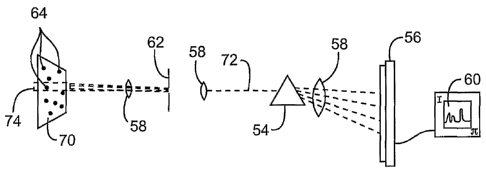
spectrum from a relatively large object by use of an aperture.
Fig. 4 schematically illustrates a method and structure for determining a
spectrum from a small object, such as an assay probe having semiconductor
nanocrystal
markers, without using an aperture.
Figs. 5A and 5B schematically illustrate a system and method for determining
absolute spectra from a plurality of semiconductor nanocrystals by limiting
the viewing field
with an aperture and by spectrally dispersing the apertured image.
Fig. 6 schematically illustrates a system and method for determining absolute
spectra of a plurality of spectrally encoded beads by simultaneously imaging
the relative
spectra of the beads, and by deriving the absolute spectra from the bead
positions.
Fig. 6A schematically illustrates a method for correlating the bead positions
and relative spectra sensed using the system of Fig. 6 to derive the absolute
spectra.
12
CA 02405267 2002-10-03
WO 01/77678 PCT/USO1/11320
Figs. 6B and 6C schematically illustrate the use of a beam splitter and
calibration signals within the spectral codes to determine the absolute
wavelengths of a
spectrum.
Figs. 7A-7C schematically illustrate a system and method for resolving
ambiguities among overlapping dispersed spectra.
Figs. 8 and 8A-8C graphically illustrates a wide variation in signal
intensities
between a spectral label and an assay marker for the exemplary probes
illustrated in Fig. 2,
and a method for identifying such signals.
Fig. 9 schematically illustrates a system and method for simultaneously
imaging a plurality of assay markers, and for sequentially scanning associated
spectral labels
for a plurality of spectrally encoded assay probes, and also illustrates the
use of differing
excitation energy sources for selectively energizing the assay markers.
Fig. 9A schematically illustrates a fluid flow assay scanning system and
method.
Figs. 10A-10C schematically illustrate a plate for positioning semiconductor
nanocrystal assay probes, together with a method for the use of positioned
probes in
multiplexed assays.
Fig. 11 schematically illustrates a method for reading the spectral labels
and/or
identifying assay results using the probe positioning plate of Fig. 10C.
DESCRIPTION OF THE SPECIFIC EMBODIMENTS
The present invention generally provides improved devices, systems, methods,
compositions of matter, kits, and the like for sensing and interpreting
spectral information.
The invention is particularly well-suited to take advantage of new
compositions of matter
which can generate signals at specific wavelengths in response to excitation
energy. A
particularly advantageous signal generation structure for use of the present
invention is the
semiconductor nanocrystal. Other useful signaling structures may also take
advantage of the
improvements provided by the present invention, including conventional
fluorescent dyes,
radiated elements and compounds, and the like.
The invention can allow efficient sensing and/or identification of a large
number of spectral codes, particularly when each code includes multiple
signals. The
invention may also enhance the reliability and accuracy with which such codes
are read, and
may thereby enable the use of large numbers of spectral codes within a
relatively small
13
CA 02405267 2002-10-03
WO 01/77678 PCT/USO1/11320
region. Hence, the techniques of the present invention will find advantageous
applications
within highly multiplexed assays, inventory control in which a large number of
small and/or
fluid elements are intermingled, and the like.
Spectral Labeling
Referring now to Fig. l, an inventory system 10 includes a library of labeled
elements 12a, 12b, . . . (collectively referred to as elements 12) and an
analyzer 14. Analyzer
14 generally includes a processor 16 coupled to a detector 18. An energy
source 20 transmits
an excitation energy 22 to a sensing field within a first labeled element 12a
of library 8. In
response to excitation energy 22, first labeled element 12a emits radiant
energy 24 defining a
spectral code. Spectral code of radiant energy 24 is sensed by detector 18 and
the spectral
code is interpreted by processor 16 so as to identify labeled element 12a.
Library 8 may optionally comprise a wide variety of elements. In many
embodiments, labeled elements 12 may be separated. However, in the exemplary
embodiment, the various labeled elements 12a, 12b, 12c, . . . are intermingled
within a test
fluid 34. Imaging is facilitated by maintaining the labeled elements on or
near a surface. As
used therein, "areal imaging" means imaging of a two-dimensional area. Hence,
fluid 34
may be contained in a thin, flat region between planar surfaces.
Preferably, detector 18 simultaneously images at least some of the signals
generated by elements 12 from within a two-dimensional sensing field. In some
embodiments, at least some of the spectral signals from within the sensing
field are
sequentially sensed using a scanning system. Regardless, maintaining each
label as a
spatially integral unit will often facilitate identification of the label.
This discrete spatial
integrity of each label is encompassed within the term "spatially resolved
labels." Preferably,
the spatial integrity of the beads and the space between beads will be
sufficient to allow at
least some of the beads to be individually resolved over all other beads,
preferably allowing
most of the beads to be individually resolved, and in many embodiments,
allowing
substantially all of the beads to be individually resolved.
The spectral coding of the present invention is particularly well-suited for
identification of small or fluid elements which may be difficult to label
using known
techniques. Elements 12 may generally comprise a composition of matter, a
biological
structure, a fluid, a particle, an article of manufacture, a consumer product,
a component for
14
CA 02405267 2002-10-03
WO 01/77678 PCT/USO1/11320
an assembly, or the like. All of these are encompassed within the term
"identifiable
substance."
The labels included with labeled elements 12 may be adhered to, applied to a
surface of, and/or incorporated within the items of interest, optionally using
techniques
analogous to those of standard bar coding technologies. For example, spectral
labeling
compositions of matter (which emit the desired spectra) may be deposited on
adhesive labels
and applied to articles of manufacture. Alternatively, an adhesive polymer
material
incorporating the label might be applied to a surface of a small article, such
as a jewel or a
component of an electronic assembly. As the information in the spectral code
does not
depend upon the aerial surface of the label, such labels can be quite small.
In other embodiments, the library will comprise fluids (such as biological
samples), powders, cells, and the like. While labeling of such samples using
standard bar
coding techniques can be quite problematic, particularly when a large number
of samples are
to be accurately identified, the spectral codes of the present invention can
allow robust
identification of a particular element from among ten or more library
elements, a hundred or
more library elements, a thousand or more library elements, and even ten
thousand or more
library elements.
The labels of the labeled elements 12 will often include compositions of
matter which emit energy with a controllable wavelength/intensity spectrum. To
facilitate
identification of specific elements from among library ~, the labels of the
elements may
include combinations of differing compositions of matter to emit differing
portions of the
overall spectral code. In other embodiments, the signals may be defined by
absorption (rather
than emission) of energy, by Raman scattering, or the like. As used herein,
the term
"markers" encompasses compositions of matter which produce the different
signals making
up the overall spectra . A plurality of markers can be combined to form a
label, with the
signals from the markers together defining the spectra for the label.
The present invention generally utilizes a spectral code comprising one or
more signals from one or more markers. The markers may comprise semiconductor
nanocrystals, with the different markers often taking the form of different
particle size
distributions of semiconductor nanocrystals having different signal generation
characteristics.
The combined markers define labels which can generate spectral codes, which
are sometimes
referred to as "spectral barcodes." These spectral codes can be used to track
the location of a
particular item of interest or to identify a particular item of interest. The
semiconductor
nanocrystals used in the spectral coding scheme can be tuned to a desired
wavelength to
CA 02405267 2002-10-03
WO 01/77678 PCT/USO1/11320
produce a characteristic spectral emission or signal by changing the
composition and/or size
of the semiconductor nanocrystal. Additionally, the intensity of the signal at
a particular
characteristic wavelength can also be varied (optionally by, at least in part,
varying a number
of semiconductor nanocrystals emitting or absorbing at a particular
wavelength), thus
enabling the use of binary or higher order encoding schemes. The information
encoded by
the semiconductor nanocrystals can be spectroscopically decoded from the
characteristics of
their signals, thus providing the location andlor identity of the particular
item or component
of interest. As used herein, wavelength and intensity are encompassed within
the term
"signal characteristics."
While spectral codes will often be described herein with reference to the
signal
characteristics of signals emitted with discrete, narrow peaks, it should be
understood that
semiconductor nanocrystals and other marker structures may generate signals
having quite
different properties. For example, signals may be generated by scattering,
absorption, or the
like, and alternative signal characteristics such as wavelength range width,
slope, shift, or the
like may be used in some spectral coding schemes.
Semiconductor Nanoc~stals
Semiconductor nanocrystals are particularly well-suited for use as markers in
a
spectral code system because of their unique characteristics. Semiconductor
nanocrystals
have radii that are smaller than the bulk exciton Bohr radius and constitute a
class of
materials intermediate between molecular and bulk forms of matter. Quantum
confinement
of both the electron and hole in all three dimensions leads to an increase in
the effective band
gap of the material with decreasing crystallite size. Consequently, both the
optical absorption
and emission of semiconductor nanocrystals shift to the blue (higher energies)
with
decreasing size. Upon exposure to a primary light source, each semiconductor
nanocrystal
distribution is capable of emitting energy in narrow spectral linewidths, as
narrow as 20-30
nm, and with a symmetric, nearly Gaussian line shape, thus providing an easy
way to identify
a particular semiconductor nanocrystal. The linewidths are dependent on the
size
heterogeneity, i.e., monodispersity, of the semiconductor nanocrystals in each
preparation.
Single semiconductor nanocrystal complexes have been observed to have full
width at half
max (FWI3M) as narrow as 12-15 nm. In addition semiconductor nanocrystal
distributions
with larger linewidths in the range of 40-60 nm can be readily made and have
the same
physical characteristics as semiconductor nanocrystals with narrower
linewidths.
16
CA 02405267 2002-10-03
WO 01/77678 PCT/USO1/11320
Exemplary materials for use as semiconductor nanocrystals in the present
invention include, but are not limited to group II-VI, III-V, and group IV
semiconductors
such as ZnS, ZnSe, ZnTe, CdS, CdSe, CdTe, GaN, GaP., GaAs, GaSb, InP, InAs,
InSb, A1S,
AlP, AISb, PbS, PbSe, Ge, Si, and ternary and quaternary mixtures or alloys
thereof. The
semiconductor nanocrystals are characterized by their nanometer size. By
"nanometer" size,
it is meant less than about 150 Angstroms (A), and preferably in the range of
12-150A.
The selection of the composition of the semiconductor nanocrystal, as well as
the size of the semiconductor nanocrystal, affects the signal characteristics
of the
semiconductor nanocrystal. Thus, a particular composition of a semiconductor
nanocrystal as
listed above will be selected based upon the spectral region being monitored.
For example,
semiconductor nanocrystals that emit energy in the visible range include, but
are not limited
to, CdS, CdSe, CdTe, and ZnTe. Semiconductor nanocrystals that emit energy in
the near 1R
range include, but are not limited to, InP, InAs, InSb, PbS, and PbSe.
Finally, semiconductor
nanocrystals that emit energy in the blue to near-ultraviolet include, but are
not limited to,
ZnS and GaN. For any particular composition selected for the semiconductor
nanocrystals to
be used in the inventive system, it is possible to tune the emission to a
desired wavelength
within a particular spectral range by controlling the size of the particular
composition of the
semiconductor nanocrystal.
In addition to the ability to tune the signal characteristics by controlling
the
size of a particular semiconductor nanocrystal, the intensities of that
particular emission
observed at a specific wavelength are also capable of being varied, thus
increasing the
potential information density provided by the semiconductor nanocrystal coding
system. In
some embodiments, 2-15 different intensities may be achieved for a particular
emission at a
desired wavelength, however, more than fifteen different intensities may be
achieved,
depending upon the particular application of the inventive identification
units. For the
purposes of the present invention, different intensities may be achieved by
varying the
concentrations of the particular size semiconductor nanocrystal attached to,
embedded within
or associated with an item or component of interest, by varying a Quantum
yield of the
nanocrystals, by varyingly quenching the signals from the semiconductor
nanocrystals, or the
like. Nonetheless, the spectral coding schemes may actually benefit from a
simple binary
structure, in which a given wavelength is either present our absent, as
described below.
In a particularly preferred embodiment, the surface of the semiconductor
nanocrystal is also modified to enhance the efficiency of the emissions, by
adding an
overcoating layer to the semiconductor nanocrystal. The overcoating layer is
particularly
17
CA 02405267 2002-10-03
WO 01/77678 PCT/USO1/11320
preferred because at the surface of the semiconductor nanocrystal, surface
defects can result
in traps for electron or holes that degrade the electrical and optical
properties of the
semiconductor nanocrystal. An insulting layer (having a bandpass layer
typically with a
bandgap energy greater than the core and centered thereover) at the surface of
the
semiconductor nanocrystal provides an atomically abrupt jump in the chemical
potential at
the interface that eliminates energy states that can serve as traps for the
electrons and holes.
This results in higher efficiency in the luminescent process.
Suitable materials for the overcoating layer include semiconductors having a
higher band gap energy than the semiconductor nanocrystal. In addition to
having a band gap
energy greater than the semiconductor nanocrystals, suitable materials for the
overcoating
layer should have good conduction and valence band offset with respect to the
semiconductor
nanocrystal. Thus, the conduction band is desirably higher and the valence
band is desirably
lower than those of the semiconductor nanocrystal. For semiconductor
nanocrystals that emit
energy in the visible (e.g., CdS, CdSe, CdTe, ZnSe, ZnTe, GaP, GaAs) or near
IR (e.g., InP,
InAs, InSb, PbS, PbSe), a material that has a band gap energy in the
ultraviolet regions may
be used. Exemplary materials include ZnS, GaN, and magnesium chalcogenides,
(e.g., MgS,
MgSe, and MgTe). For semiconductor nanocrystals that emit in the near lR,
materials having
a band gap energy in the visible, such as CdS, or CdSe, may also be used.
While the
overcoating will often have a higher bandgap than the emission energy, the
energies can be,
for example, both within the visible range. The overcoating layer may include
as many as 8
monolayers of the semiconductor material. The preparation of a coated
semiconductor
nanocrystal may be found in U.S. Patent Application No. 08/969,302 filed
November 13,
1997, entitled "Highly Luminescent Color-Selective Materials"; Dabbousi et
al., J. Phi
Chem B., Vol. 101, 1997, pp. 9463; and Kuno et al., J. Phys. Chem., Vol. 106,
1997, pp.
9869. Fabrication and combination of the differing populations of
semiconductor
nanocrystals may be further understood with reference to U.S. Patent
Application No.
09/397,432, previously incorporated herein by reference.
It is often advantageous to combine different markers of a label into one or
more labeled body. Such labeled bodies may help spatially resolve different
labels from
intermingled items of interest, which can be beneficial during identification.
These label
bodies may comprise a composition of matter including a polymeric matrix and a
plurality of
semiconductor nanocrystals, which can be used to encode discrete and different
absorption
and emission spectra. These spectra can be read using a light source to cause
the label bodies
to absorb or emit light. By detecting the light absorbed and/or emitted, a
unique spectral code
18
CA 02405267 2002-10-03
WO 01/77678 PCT/USO1/11320
may be identified for the labels. In some embodiments, the labeled bodies may
further
include markers beyond the label bodies. These labeled bodies will often be
referred to as
"beads" herein, and beads which have assay capabilities may be called
"probes." The
structure and use of such probes, including their assay capabilities, are more
fully described
in U.S. patent application no. 09/566,014, previously incorporated herein by
reference.
Fabrication of Labeled Beads
Referring now to Fig. 2, first and second labeled elements 12a, 12b within
test
fluid 34 are formed as separate semiconductor nanocrystal probes 34'. Each
probe includes
an associated label 36 formed from one or more populations of substantially
mono-disperse
semiconductor nanocrystals 37. The individual populations of semiconductor
nanocrystals
will often be mono-disperse so as to provide a sufficient signal intensity at
a uniform
wavelength for convenient sensing of the various signals within the code. The
exemplary
probes further include one or more binding moieties 35', together with a probe
matrix or body
material 39, which acts as a binding agent to keep the various marlcers
together in a structural
unit or bead. Binding moieties 35' help (indirectly) to generate signals
indicating results of
an assay, each probe moiety having selective affinity for an associated test
substance 35
which may be present within sample fluid 34. Probe moieties 35' may comprise
an antibody,
DNA, or the like, and test substances 35 may carry reporters or assay markers
38 for
generating signals indicating results of the assays. Alternatively, the assay
markers may have
selective affinity for the combination of a particular test substance and
bound probe moiety,
or the like. Preparation of the spectrally encoded probes will now be
described, followed by
a brief description of the use and structure of assay markers 38.
A process for encoding spectra into label body materials using a feedback
system can be based on the absorbance and luminescence of the semiconductor
nanocrystals
in a solution that can be used to dye the materials. More specifically, this
solution can be
used for encoding of a plurality of semiconductor nanocrystals into a material
when that
material is a polymeric bead.
A variety of different materials can be used to prepare these compositions. In
particular, polymeric bead materials are an appropriate format for efficient
multiplexing and
demultiplexing of finite-sized materials. These label body beads can be
prepared from a
variety of different polymers, including but not limited to polystyrene, cross-
linked
polystyrene, polyacrylic, polysiloxanes, polymeric silica, latexes, dextran
polymers, epoxies,
and the like. The materials have a variety of different properties with regard
to swelling and
19
CA 02405267 2002-10-03
WO 01/77678 PCT/USO1/11320
porosity, which are well understood in the art. Preferably, the beads are in
the size range of
approximately 10 nm to 1 mm, more preferably in a size range of approximately
100 nm to
O.lmm, often being in a range from 1000 nm to 10,000 nm, and can be
manipulated using
normal solution techniques when suspended in a solution.
Discrete emission spectra can be encoded into these materials by varying the
amounts and ratios of different semiconductor nanocrystals, either the size
distribution of
semiconductor nanocrystals, the composition of the semiconductor nanocrystals,
or other
property of the semiconductor nanocrystals that yields a distinguishable
emission spectrum,
which are embedded into, attached to or otherwise associated with the
material. The
semiconductor nanocrystals of the invention can be associated with the
material by
adsorption, absorption, covalent attachment, by co-polymerization or the like.
The
semiconductor nanocrystals have absorption and emission spectra that depend on
their size
and composition. These semiconductor nanocrystals can be prepared as described
in Murray
et. al., (1993) J. Am. Chem. Soc. 115:8706-8715; Guzelian et. al., (1996) J.
PhDs. Chem.
100;7212-7219; or International Publication No. WO 99/26299 (inventors Bawendi
et al.).
The semiconductor nanocrystals can be made further luminescent through
overcoating
procedures as described in Danek et. al., (1966) Chern. Mat. 8(1):173-180;
Hines et. al.,
(1996) J. Phys. Chem. 100:468-471; Peng et. al., (1997) J. Am. Chem. Soc.
119:7019-7029;
or Daboussi et. al., (1997) J. Phys. Chem.-B, 101:9463-9475.
The desired spectral emission properties may be obtained by mixing
semiconductor nanocrystals of different sizes and/or compositions in a fixed
amount and ratio
to obtain the desired spectrum. The spectral emission of this staining
solution can be
determined prior to treatment of the material therewith. Subsequent treatment
of the material
(through covalent attachment, co-polymerization, passive absorption, swelling
and
contraction, or the like) with the staining solution results in a material
having the designed
spectral emission property. These spectra may be different under different
excitation sources.
Accordingly, it is preferred that the light source used for the encoding
procedure be as similar
as possible (preferably of the same wavelength and/or intensity) to the light
source that will
be used for the decoding. The light source may be related in a quantitative
manner, so that
the emission spectrum of the final material may be deduced from the spectrum
of the staining
solution.
A number of semiconductor nanocrystal solutions can be prepared, each
having a distinct distribution of sizes and compositions, and consequently a
distinct enussion
spectrum, to achieve a desired emission spectrum. These solutions may be mixed
in fixed
CA 02405267 2002-10-03
WO 01/77678 PCT/USO1/11320
proportions to arrive at a spectrum having the predetermined ratios and
intensities of
emission from the distinct semiconductor nanocrystals suspended in that
solution. Upon
exposure of this solution to a light source, the emission spectrum can be
measured by
techniques that are well established in the art. If the spectrum is not the
desired spectrum,
then more of a selected semiconductor nanocrystal solution can be added to
achieve the
desired spectrum and the solution titrated to have the correct emission
spectrum. These
solutions may be colloidal solutions of semiconductor nanocrystals dispersed
in a solvent, or
they may be pre-polymeric colloidal solutions, which can be polymerized to
foam a matrix
with semiconductor nanocrystals contained within. While ratios of the
quantities of
constituent solutions and the final spectrum intensities need not be the same,
it will often be
possible to derive the final spectra from the quantities (and/or the
quantities from the desired
spectra.)
The solution luminescence will often be adjusted to have the desired
intensities and ratios under the exact excitation source that will be used for
the decoding. The
spectrum may also be prepared to have an intensity and ratio among the various
wavelengths
that are known to produce materials having the desired spectrum under a
particular excitation
source. A multichannel auto-pipettor connected to a feedback circuit can be
used to prepare a
semiconductor nanocrystal solution having the desired spectral
characteristics, as described
above. If the several channels of the titrator/pipettor are charged or loaded
with several
unique solutions of semiconductor nanocrystals, each having a unique
excitation and
emission spectrum, then these can be combined stepwise through addition of the
stock
solutions. In between additions, the spectrum may be obtained by exposing the
solution to a
light source capable of causing the semiconductor nanocrystals to emit,
preferably the same
light source that will be used to decode the spectra of the encoded materials.
The spectrum
obtained from such intermediate measurements may be judged by a computer based
on the
desired spectrum. If the solution luminescence is lacking in one particular
semiconductor
nanocrystal emission spectrum, stock solution containing that semiconductor
nanocrystal may
be added in sufficient amount to bring the emission spectrum to the desired
level. This
procedure can be carried out for all different semiconductor nanocrystals
simultaneously, or it
may be carried out sequentially.
Once the staining solution has been prepared, it can be used to incorporate a
unique luminescence spectrum into the materials of this invention. If the
method of
incorporation of the semiconductor nanocrystals into the materials is
absorption or
adsorption, then the solvent that is used for the staining solution may be one
that is suitable
21
CA 02405267 2002-10-03
WO 01/77678 PCT/USO1/11320
for swelling the materials. Such solvents are commonly from the group of
solvents including
dichloromethane, chloroform, dimethylformamide, tetrahydrofuran and the like.
These can
be mixed with a more polar solvent, for example methanol or ethanol, to
control the degree
and rate of incorporation of the staining solution into the material. When the
material is added
to the staining solution, the material will swell, thereby causing the
material to incorporate a
plurality of semiconductor nanocrystals in the relative proportions that are
present in the
staining solution. In some embodiments, the semiconductor nanocrystals may be
incorporated
in a different but predictable proportion. When a more polar solvent is added,
after removal
of the staining solution from the material, material shrinks, or unswells,
thereby trapping the
semiconductor nanocrystals in the material. Alternatively, semiconductor
nanocrystals can be
trapped by evaporation of the swelling solvent from the material. After
rinsing with a solvent
in which the semiconductor nanocrystals are soluble, yet that does not swell
the material, the
semiconductor nanocrystals are trapped in the material, and may not be rinsed
out through the
use of a non-swelling, non-polar solvent. Such a non-swelling, non-polar
solvent is typically
hexane or toluene. The materials can be separated and then exposed to a
variety of solvents
without a change in the emission spectrum under the light source. When the
material used is
a polymer bead, the material can be separated from the rinsing solvent by
centrifugation or
evaporation or both, and can be redispersed into aqueous solvents and buffers
through the use
of detergents in the suspending buffer, as is well known in the art.
The above procedure can be carried out in sequential steps as well. A first
staining solution can be used to stain the materials with one population of
semiconductor
nanocrystals. A second population of semiconductor nanocrystals can be
prepared in a
second staining solution, and the material exposed to this second staining
solution to
associate the semiconductor nanocrystals of the second population with the
material. These
steps can be repeated until the desired spectral properties are obtained from
the material when
excited by a light source, optionally using feedback from measurements of the
interim spectra
generated by the partially stained bead material to adjust the process.
The semiconductor nanocrystals can be attached to the material by covalent
attachment, and/or by entrapment in pores of the swelled beads. For instance,
semiconductor
nanocrystals are prepared by a number of techniques that result in reactive
groups on the
surface of the semiconductor nanocrystal. See, e.g., Bruchez et. al., (1998)
Science
281:2013-2016; and Ghan et. al., (1998) Science 281:2016-2018, Golvin et. al.,
(1992) J. Am.
Chem. Soc. 114:5221-5230; Katari et. al. (1994) J. Phys. Chem. 98:4109-4117;
Steigerwald
et. al. (1987) J. Am. Chem. Soc. 110:3046. The reactive groups present on the
surface of the
22
CA 02405267 2002-10-03
WO 01/77678 PCT/USO1/11320
semiconductor nanocrystals can be coupled to reactive groups present on the
surface of the
material. For instance, semiconductor nanocrystals which have carboxylate
groups present
on their surface can be coupled to beads with amine groups using a carbo-
diimide activation
step, or a variety of other methods well known in the art of attaching
molecules and
biological substances to bead surfaces. In this case, the relative amounts of
the different
semiconductor nanocrystals can be used to control the relative intensities,
while the absolute
intensities can be controlled by adjusting the reaction time to control the
number of reacted
sites in total. After the bead materials are stained with the semiconductor
nanocrystals, the
materials are optionally rinsed to wash away unreacted semiconductor
nanocrystals.
Referring once again to Fig. 2, labeled elements 12a, 12b (here in the form of
semiconductor nanocrystal probes) may be useful in assays in a wide variety of
forms. Utility
of the probes for assays benefits significantly from the use of moieties or
affinity molecules
35', as schematically illustrated in Fig. 2, which may optionally be supported
directly by a
label marker 37 of label 36, by the probe body matrix 39, or the like.
Moieties 35' can have
selective affinity for an associated detectable substance 35, as schematically
illustrated by
correspondence symbol shapes in Fig. 2. The probes may, in some embodiments,
also
include an integrated assay marker 38 which is activated or enabled to
generate a signal by
the binding of probe moiety 35' to test substance 35. In many embodiments, the
assay marker
will instead be coupled to the probes by coupling of detectable substance 35
to moiety 35'.
In other words, the assay marker 38 may (at least initially) be coupled to the
detectable
substance 35, typically by binding of a dye molecule, incorporation of a
radioactive isotope,
or the like. The assay markers may thus be coupled to the probe by the
interaction between
the moieties 35' and the test or detectable substances 35. In other assays,
the assay results
may be determined by the presence or absence of the probe or bead (for
example, by washing
away probes having an unattached moiety) so that no dedicated assay marker
need be
provided.
In alternative embodiments, the material used to make the codes does not need
to be semiconductor nanocrystals. For example, any fluorescent material or
combination of
fluorescent materials that can be finely tuned throughout a spectral range and
can be excited
optically or by other means might be used. For organic dyes, this may be
possible using a
number of different dyes that are each spectrally distinct.
This bead preparation method can be used generically to identify identifiable
substances, including cells and other biological matter, objects, and the
like. Pre-made
mixtures of semiconductor nanocrystals, as described above, axe attached to
objects to render
23
CA 02405267 2002-10-03
WO 01/77678 PCT/USO1/11320
them subsequently identifiable. Many identical or similar objects can be coded
simultaneously, for example, by attaching the same semiconductor nanocrystal
mixture to a
batch of microspheres using a variety of chemistries known in the art.
Alternatively, codes
may be attached to objects individually, depending on the objects being coded.
In this case,
the codes do not have to be pre-mixed and may be mixed during application of
the code, for
example using an inkjet printing system to deliver each species of
semiconductor
nanocrystals to the object. The use of semiconductor nanocrystal probes in
chemical and/or
biological assays is more fully described in U.S. Patent Application No.
09/566,014, the full
disclosure of which is incorporated herein by reference.
The semiconductor nanocrystal probes of Fig. 2 may also be utilized to detect
the occurrence of an event. This event, for example, may cause the source from
which energy
is transferred to assay marker 38 to be located spatially proximal to the
semiconductor
nanocrystal probe. Hence, the excitation energy from energy source 20 may be
transferred
either directly to assay markers 38, 38', or indirectly via excitation of one
or more energy
sources adjacent the semiconductor nanocrystal probes due to bonding of the
test substances
35 to the moiety 35'. For example, a laser beam may be used to excite a
proximal source
such as a semiconductor nanocrystal probe 38' attached to one of the test
substances 35 (to
which the affinity molecule selectively attaches), and the energy emitted by
this
semiconductor nanocrystal 38' may then excite an assay marker 38 affixed to
the probe
matrix. As mentioned above, still further assay marker structures and methods
are described
in detail in co-pending U.S. Patent Application No. 09/566,014.
Readin.~ Beads
Referring once again to Fig. 1, energy source 20 generally directs excitation
energy 22 in such a form as to induce emission of the spectral code from
labeled element 12a.
In one embodiment, energy source 20 comprises a source of light, the light
preferably having
a wavelength shorter than that of the spectral code. Energy source 20 may
comprise a source
of blue or ultraviolet light, optionally comprising a broad band ultraviolet
light source such a
deuterium lamp, optionally with a filter. Alternatively, energy source 20 may
comprise an
Xe or Hg UV lamp, or a white light source such as a xenon lamp or a deuterium
lamp,
preferably with a short pass or bandpass filter disposed along the excitation
energy path from
the lamp to the labeled elements 12 so as to limit the excitation energy to
the desired
wavelengths. Still further alternative excitation energy sources include any
of a number of
continuous wave (cw) gas lasers, including (but not limited to) any of the
argon ion laser
24
CA 02405267 2002-10-03
WO 01/77678 PCT/USO1/11320
lines (457 nm, 488 nm, 514 nm, etc.), a HeCd laser, a solid-state diode laser
(preferably
having a blue or ultraviolet output such as a GaN based laser, a GaAs based
laser with
frequency doubling, a frequency doubled or tripled output of a YAG or YLF
based laser, or
the like), any of the pulsed lasers with an output in the blue or ultraviolet
ranges, light
emitting diodes, or the like, or any other laser source (solid, liquid, or gas
based) with
emissions to the blue of the code spectrum.
The excitation energy 22 from energy source 20 will induce labeled element
12a to emit identifiable energy 24 having the spectral code, with the spectral
code preferably
comprising signals having relatively narrow peaks so as to define a series of
distinguishable
peak wavelengths and associated intensities. The peaks will typically have a
half width of
about 100 nm or less, preferably of 70 nm or less, more preferably 50 nm or
less, and ideally
30 nm or less. In many embodiments, a plurality of separate signals will be
included in the
spectral code as sensed by sensor 18. As semiconductor nanocrystals are
particularly well-
suited for generating luminescent signals, identifiable energy 24 from label
12a will often
comprise light energy. To help interpret the spectral code from the
identifiable energy 24, the
light energy may pass through one or more monochromator or other wavelength
dispersive
element. A Charge-Coupled Device (CCD) camera or some other two-dimensional
detector
of sensor 18 can sense and/or record the images for later analysis. In other
embodiments, a
scanning system maybe employed, in which the labeled element to be identified
is scanned
with respect to a microscope objective, with the luminescence put through a
single
monochromator or a grating or prism to spectrally resolve the colors. The
detector can be a
diode array that records the colors that are emitted at a particular spatial
position, a two-
dimensional CCD, or the like.
Information regarding these spectra from the labeled elements 12 will
generally be transmitted from sensor 18 to processor 16, the processor
typically comprising a
general purpose computer. Processor 16 will typically include a central
processing unit,
ideally having a processing capability at least equivalent to a Pentium
I° processor, although
simpler systems might use processing capabilities of a Palm" handheld
processor or more.
Processor 16 will generally have input and output capabilities and associated
peripheral
components, including an output device such as a monitor, an input such as a
keyboard,
mouse, and/or the like, and will often have a networking connection such as an
Ethernet, an
Intranet, an Internet, andlor the like. An exemplary processing block diagram
is
schematically illustrated in Fig. 1A.
CA 02405267 2002-10-03
WO 01/77678 PCT/USO1/11320
Processor 16 will often make use of a tangible media 30 having a machine-
readable code embodying method steps according to one or more methods of the
present
invention. A database 32, similarly embodied on a machine-readable code, will
often include
a listing of the elements included in library 8, the spectral codes of the
labels associated with
the elements, and a correlation between specific library elements and their
associated codes.
Processor 16 uses the information from database 32 together with the spectrum
characteristics
sensed by sensor 18 to identify a particular library element 12a. The machine-
readable code
of program instructions 30 and database 32 may take a wide variety of forms,
including
floppy disks, optical discs (such as CDs, DVDs, rewritable CDs, and the like),
alternative
magnetic recording media (such as tapes, hard drives, and the like), volatile
and/or non-
volatile memories, software, hardware, firmware, or the like.
As illustrated in Fig. 1, methods for detecting and classifying spectral
labels
(such as encoded materials and beads) may comprise exposing the labels to
light of an
excitation source so that the semiconductor nanocrystals of the label are
sufficiently excited
to emit light. This excitation source is preferably of an energy capable of
exciting the
semiconductor nanocrystals to emit light and may be of higher energy (and
hence, shorter
wavelength) than the shortest emission wavelength of the semiconductor
nanocrystals in the
label. Alternatively the excitation source can emit light of longer wavelength
if it is capable
of exciting some of the semiconductor nanocrystals disposed in the matrix to
emit light, such
as using two-photon excitation. This excitation source is preferably chosen to
excite a
sufficient number of different populations of semiconductor nanocrystals to
allow unique
identification of the encoded materials. For example, using materials stained
in a 1:2 ratio of
red to blue and a 1:3 ratio of red to blue, it may not be sufficient to only
excite the red
emitting semiconductor nanocrystals (e.g., by using green or yellow light) of
the sample in
order to resolve these beads. It would be desirable to use a light source with
components
that are capable of exciting the blue emitting and the red emitting
semiconductor nanocrystals
simultaneously, (e.g., violet or ultraviolet). There may be one or more Iight
sources used to
excite the populations of the different semiconductor nanocrystals
simultaneously or
sequentially, but each light source may selectively excite sub-populations of
semiconductor
nanocrystals that emit at Iower energy than the Iight source (to a greater
degree than higher
energy emitting sub-populations), due to the absorbance spectra of the
semiconductor
nanocrystals. Ideally, a single excitation energy source will be sufficient to
induce the labels
to emit identifiable spectra.
26
CA 02405267 2002-10-03
WO 01/77678 PCT/USO1/11320
Spectral Codes
Refernng now to Figs. 2A-2E, the use of a plurality of different signals
within
a single spectral label can be understood. In this simple example, a coding
system is shown
having two signals. A first signal has a wavelength peak 40a at a first
discreet wavelength,
while a separate signal has a different wavelength peak 40b. As shown in Figs.
2A-2D,
varying peak 40b while the first peak 40a remains at a fixed location defines
a first family of
spectral codes 1a through 4a. Moving the first peak 40a to a new location
allows a second
family of spectral codes to be produced, as can be understood with reference
to Fig. 2E.
The simple code system illustrated in Figs. 2A-2E includes only two signals,
but still allows a large number of identifiable spectra. More complex spectral
codes having
larger numbers of peaks can significantly increase the number of codes.
Additionally, the
intensities of one or more of the peaks may also be varied, thereby providing
still higher
order codes having larger numbers of separately identifiable members.
Spectral Code Reading S s
In general, fluorescent labeling is a powerful technique for tracking
components in biological systems. For instance, labeling a portion of a cell
with a fluorescent
marker can allow one to monitor the movement of that component within the
cell. Similarly,
labeling an analyte in a bioassay can allow one to determine its presence or
absence, even at
vanishingly small concentrations. The use of multiple fluorophores with
different emission
wavelengths allows different components to be monitored simultaneously.
Applications such
as spectral encoding can take full advantage of multicolor fluorophores,
potentially allowing
the simultaneous detection of millions of analytes.
When imaging samples labeled with multiple chromophores, it is desirable to
resolve spectrally the fluorescence from each discrete region within the
sample. As an
example, an assay may be prepared in which polymer beads have been labeled
with two
different chromophores and the results of the assay may be determined by the
ratio of the two
types of beads within the final sample. One could imagine immobilizing the
beads and
counting each of the colors. Electronic imaging requires a technique for
acquiring an image
of the sample in which spectral information is available at each discrete
point. While the
human eye is exceptionally good at distinguishing colors, typical electronic
photodetectors
are often effectively color-blind. As such, additional optical components are
often used in
order to acquire spectral information.
27
CA 02405267 2002-10-03
WO 01/77678 PCT/USO1/11320
Many techniques might be applied to solve this problem. Fourier transform
spectral imaging (Malik et al. (1996) J. Microsc. 182:133; Brenan et al.
(1994) Appl. Opt
33:7520) and Hadamard transform spectral imaging (Treado et al. (1989) Anal.
Chem
61:732A; Treado et al. (1990) Ap~l. Spectrosc. 44:1-4; Treado et al. (1990)
Appl. Spectrosc.
44:1270; Hammaker et al. (1995) J. Mol. Struct. 348:135; Mei et al. (1996) J.
Anal. Chem.
354:250; Flateley et al. (1993) April. Spectrosc. 47:1464), imaging through
variable
interference (Youvan (1994) Nature 369:79; Goldman et al. (1992) Biotechnolo~y
10:1557),
acousto-optical (Mortensen et al. (1996) IEEE Trans. Inst. Meas. 45:394;
Turner et al (1996)
Appl. Spectrosc. 50:277) or liquid crystal filters (Morris et al. (1994) Appl.
Spectrosc.
48:857) or simply scanning a slit or point across the sample surface
(Colarusso et al. (1998)
Anpl. Spectrosc. 52:106A) are methods capable of generating spectral and
spatial information
across a two-dimensional region of a sample. Most of these techniques,
however, benefit
from the mechanical scanning of one component of the system as well as the
acquisition of
multiple data frames in order to generate a spectral image. For instance,
Fourier transform
imaging scans an interferometer, acquiring a full image at each mirror
position. The spectral
information is then extracted from the complete set of spatial images.
Similarly, "point
scanning" typically relies on a full spectrum from each position within the
image and scans
all positions to generate the full image. These techniques may allow precise
spectral fitting
and analysis, but may be too cumbersome and slow for highly multiplexed
systems.
Referring now to Fig. 3, a system and method for reading spectral information
from an arbitrarily large object 50 generally makes use of a detector 52
including a
wavelength dispersive element 54 and a sensor 56. Imaging optics 58 image
object 50 onto a
surface of sensor 56. Wavelength dispersive element 54 spectrally disperses
the image across
the surface of the sensor, distributing the image based on the wavelengths of
the image
spectra.
As object 50 is relatively large when imaged upon sensor 56, differentiation
of
the discreet wavelengths within a spectrum 60 is facilitated by the use of an
aperture 62. As
aperture 62 allows only a small region of the image through wavelength
dispersive element
54, the wavelength dispersive element separates the image components based on
wavelength
alone (rather than on a combination of wavelength and position along the
surface of image
50). Spectra 60 may then be directly determined based on the position of the
diffracted
image upon sensor 56, together with the intensity of image wavelength
components as
measured by the sensor. As the position of object 50 is scanned past aperture
62, the
remainder of the spectral image can be collected. Referring now to Fig. 4, a
spectra 60 of a
28
CA 02405267 2002-10-03
WO 01/77678 PCT/USO1/11320
spectrally labeled nanocrystal bead 64 may be performed using a detector 66
without an
aperture. As bead 64 has a signal generating area (as imaged by imaging optics
58) which is
much smaller than a sensing surface of sensor 56, bead 64 can act as a point-
source of spectra
60. Optics 58 would typically, in the absence of dispersive element 54, image
bead 64 on
detector 56 so that the bead image has a size similar to or smaller than an
aperture of a
monochrometer (the undispensed image size typically being about 250 p.m or
less, ideally
about 120 ~.m or less). The various signals of the spectral code emanate from
small surface
area of the bead, so that the signal distribution across the sensor surface is
dominated by the
wavelength dispersion, and no limiting of the image via an aperture is
required. As used
herein, a "true point source" is a light source with a dimension which is at
least as small as a
minimum, diffraction limited determinable dimension. A light source which is
larger than a
true point source may be "treated" or "analyzed" as a point source if it has a
dimension or
size which is sufficiently small that its size acts like an aperture.
As described above, it will often be advantageous to include a plurality of
different spectrally labeled beads within a fluid. These labeled beads will
often be supported
by the surrounding fluid, and/or will be movable with the fluid, particularly
in high-
throughput multiplexed bead-based assays. Optionally, the beads may have a
size sufficient
to define a suspension within the surrounding test fluid. In some embodiments,
the beads
may comprise a colloid within the test fluid. In some embodiments, beads 64
may be
movably supported by a surface of a vessel containing the test fluid, for
example, being
disposed on the bottom surface of the vessel (where probe 64 has a density
greater than that
of the test fluid). In other embodiments, the beads may be affixed to a
support structure
and/or to each other. Still further alternatives are possible, such as for
probe 64 to be floating
on an upper surface of the test fluid, for the bead or beads to be affixed to
or disposed
between cooperating surfaces of the vessel to maintain the positioning of the
bead or beads,
for the bead or beads to be disposed at the interface between two fluids, and
the like.
As was described above, it will often be advantageous to include numerous
beads 64 within a single test fluid so as to perform a plurality of assays.
Similarly, it will
often be advantageous to identify a large number of fluids or small discreet
elements within a
single viewing area without separating out each spectral label from the
combined labeled
elements. As illustrated in Fig. 4, the dispersed spectral image 68 of bead 64
upon sensor 56
will depend on both the relative spectra generated by the bead, and on the
position of the
bead. For example, bead 64' is imaged onto a different portion 68' of sensor
56, which could
29
CA 02405267 2002-10-03
WO 01/77678 PCT/USO1/11320
lead to misintezpretation of the wavelengths of the spectra if the location of
bead 64' is not
known. So long as an individual bead 64 can be accurately aligned with the
imaging optics
58 and sensor system 66, absolute spectral information can be obtained.
However, as can be
understood with reference to Fig. 5A, a plurality of beads 64 will often be
distributed
throughout an area 70.
To ensure that only beads 64 which are aligned along an optical axis 72 are
imaged onto sensor 56, aperture 62 restricts a sensing field 74 of the sensing
system. Where
sensor 56 comprises an areal sensor such a charge couple device (CCD),
aperture 62 may
comprise a slit aperture so that spectral wavelengths ~, can be determined
from the position of
the dispersed images 68 along a dispersion axis of wavelength dispersive
element 54 for
multiple beads 64 distributed along the slit viewing field 74 along a second
axis y, as can be
understood with reference to Fig. 5B. Absolute accuracy of the spectral
readings will vary
inversely with a width of aperture slit 62, and the number of readings (and
hence total reading
time) for reading all the beads in area 70 will be longer as the slit gets
narrower.
Nonetheless, the beads 64 within the two-dimensional area 70 may eventually be
read by the
system of Figs. 5A and 5B with a scanning system which moves the slit relative
to beads 64
(using any of a variety of scanning mechanisms, such as movable mirrors, a
movable
aperture, a flow of the beads passed a fixed aperture, a movement of the
surface of the vessel
relative to the aperture, or the like).
While the techniques described above are capable of producing spectral
images, there are at least two distinct disadvantages to most scanning
systems. First, most
scanning systems are susceptible to mechanical or electronic failure that
would not exist in a
static (non-scanning) system. Second, since many data points are used to
generate a single
spectral image, a limit is placed on the minimum time required in order to
acquire a full
image. Depending on the signal levels, this time could be several minutes or
more. This
generally precludes the use of scanning techniques in any system in which the
spatial position
of each point is not fixed. For instance, imaging the two-color beads
described above in an
aqueous medium may be difficult with a scanning system, since the beads can
diffuse to
different spatial positions during the acquisition of a single spectral image.
Static spectral imaging systems, in which spectral information is acquired
without scanning, are very appealing since data is acquired in a single step.
An example of a
static spectral imaging system is one in which a spatial image is passed
though several beam-
splitters, separating it into multiple images, each of which is passed though
a different band-
CA 02405267 2002-10-03
WO 01/77678 PCT/USO1/11320
pass filter. Each resulting image provides information about a discrete region
of the spectrum.
The images are then projected onto a detector and the signals are recombined
to produce an
image that contains information about the amount of light within each band-
pass. Such
systems are appealing because all spectxal information may be acquired
simultaneously,
eliminating difficulties arising from non-stationary samples. The disadvantage
of a band-pass
imaging system is that only a discrete number of wavelengths can be monitored,
precluding
detailed spectral analysis and fitting. At the same time, band-pass filters
and dichroic mirrors
are not 100% efficient, reducing the potential detection efficiency of
multiple colors. For
instance, a band-pass system using ten 10% beamsplitters and 10 bandpass
filters results in a
maximum of 10% detection efficiency along each channel. A system of dichroic
mirrors,
each with 85% transmission efficiency yields approximately 20% efficiency
along the final
channel.
Referring once again to Figs. 5A and 5B, one-dimensional spectral imaging
can be achieved by projecting a fluorescent image onto andlor through the
entrance slit of a
linear spectrometer, as shown. In this configuration, spatial information is
retained along the
y-axis, while spectral information (wavelengths ~,) is dispersed along the x-
axis, as described
by Empedocles, et al. in Ph~s. Rev. Lett., 77 (18); p. 3873 (1996). The
entrance slit restricts
the spatial position of the light entering the spectrometer, thereby (at least
in part) defining
the calibration for each spectrum. The width of the entrance slit, in part,
defines the spectral
resolution of the system.
Refernng now to Fig. 6, a two-dimensional imaging system 80 allows
simultaneous sensing of spectral information from bead 64 distributed
throughout a two-
dimensional sensing field 81. System 80 generally makes use of a detector 82
and a system
for restraining and/or identifying a position of beads 64 within two-
dimensional sensing field
81. In the exemplary embodiment, the positioning system or means makes use of
a bead
position indicator 84. Positioning indicator 84 is optically coupled to
sensing field 81. More
specifically, a beam splitter 86 separates a portion of an image generated by
optical train 58,
and directs the image portion 88 onto a position sensor. As described above,
detector 82
makes use of a wavelength dispersive element 54 and an areal sensor 56 aligned
with optical
train 58, hence, at least a portion of the optical path between two-
dimensional sensing field
81 and the positioning system 84 is coaxial with the optical path between the
sensing field 81
and sensor 56 of the detector 82.
31
CA 02405267 2002-10-03
WO 01/77678 PCT/USO1/11320
As beads 64 are distributed across two-dimensional sensing field 81 and are
not limited to a single lateral axis, wavelength dispersive element 54 will
distribute the
spectra from beads 64 across the surface of sensor 56 based on both the
wavelength of the
spectra from each bead and the associated position of the bead within the
sensing field.
Where beads 64 are sufficiently small in area so as to be treated as point-
light sources, and
where there is significantly more area surrounding the beads than the total
surface area of the
beads themselves so that the distributed spectra from the labels on the beads
do not overlap
excessively, sensor 56 can be used to determine relative spectra of the beads.
For example,
analyzer 90, in response to signals from sensor 56, may determine that a
particular bead 64a
has three equally-spaced wavelength peaks of substantially even intensity,
with a fourth
wavelength peak of twice the intensity of the other peaks separated from the
lowest of the
peaks by three times the wavelength differential between the other peaks.
While such
relative spectral information is useful (and may be sufficient to identify
codes in some coding
systems) it will often be advantageous to provide both relative and absolute
spectral
information for each of beads 64.
Fortunately, positioning image 88 generated upon a sensor surface 92 of
position indicator 84 defines the position of beads 64 within sensing field
81. Signals
transmitted from the sensor of position indicator 84 to analyzer 90 can define
positions for
each bead 64, and the analyzer can correlate each bead position with its
associated spectra
(and hence the sensed relative spectra) to determine the absolute spectrum
from each bead.
By taking advantage of the point-light source qualities of the relatively
small beads within
sensing field 81, no aperture need be included within two-dimensional system
80. In some
embodiments, the positioning image and the spectrally disbursed image may be
projected
onto a common sensor, either sequentially or on different positions of the
common sensor.
Still further alternatives are possible, such as the projection of a zero-
order image on the CCD
for spatial information.
Stated differentially, two-dimensional images can be obtained by eliminating
the entrance slit from a linear spectrometer and allowing the discrete images
from individual
points to define the spatial position of the light entering the spectrometer
(Fig. 6). In this case,
the spectral resolution of the system is defined, in part, by the size of the
discrete images.
Since the spatial position of the light from each point varies across the x-
axis, however, the
calibration for each spectrum will be different, resulting in an error in the
absolute energy
values. Splitting the original image and passing one half through a dispersive
grating to create
a separate image and spectra can eliminate this calibration error. With
appropriate alignment,
32
CA 02405267 2002-10-03
WO 01/77678 PCT/USO1/11320
a correlation can be made between the spatial position and the absolute
spectral energy (Fig.
6A).
Correlation of the positioning image 88 with the spectrally dispersed image 68
can be understood with Figs. 6A through 6C. Positioning image 88 generally
indicates
positions of beads 64 within sensing field 81, while spectrally dispersed
image 68 reflects
both the position and spectral wavelengths of each signal within the spectra
generated by
beads 64. Using an accurately calibrated system, analyzer 90 can determine the
absolute
wavelengths of a particular dispersed image 96a by identifying the associated
bead position
64a, particularly where beads 64 do not overlap along the y-axis. As can be
understood with
reference to Figs. 6B and 6C, correlation of beads' locations and spectrally
dispersed images
may be facilitated by including a calibration signal 40c within at least one
of the spectra
generated by a bead. Such calibration signals will often be included in at
least some of the
bead spectra, optionally being included in each bead spectrum. Where the
calibration signal
wavelength is known, the location of the associated bead along the x-axis can
be determined
from the location of the calibration signal energy within the dispersed image
68 from the
diffracting characteristics of wavelength dispersive element 54.
Referring now to Figs. 7A-7C, ambiguity may arise when images of beads 64
fall along and/or adjacent to a dispersion axis, along a horizontal line in
the example of Fig.
7A. To avoid such ambiguity, an alternative two-dimensional spectral sensing
system 80'
includes an additional beam splitter 86' with a second dispersive element or
wavelength
dispersive element 54', with the second wavelength dispersive element having a
diffraction
axis oriented at an angle to the dispersive axis of the first wavelength
dispersive element 54
relative to the image of the two-dimensional sensing field 81. Typically, the
second
wavelength dispersive element will have a dispersive axis oriented at
90° to the dispersive
axis of the first wavelength dispersive element, although any angle between
0° and 180°
could be used. This second wavelength dispersive element generates a dispersed
image 68'
along the second dispersive axis (typically orthogonal to the first dispersive
axis), allowing
analyzer 60 to unambiguously distinguish the spectra from each discrete point
within the
image. In related embodiments, two orthogonal (or otherwise angularly offset)
dispersive
elements may be disposed along the same imaging path, or possibly even fowled
together to
disperse a single image spectrally along two offset dispersive axes. The tow
offset spectra
may be imaged onto a single sensor. Positions of the beads may be determined
from the
33
CA 02405267 2002-10-03
WO 01/77678 PCT/USO1/11320
intersections of each spectral pair, so that a processor derives the position
form the combined
images 68 and 68', as can be understood with reference to Fig. 7C.
In the preferred embodiment, the original image is split into 2 (or 3) images
at
ratios that provide more light to the spectrally dispersed images, which have
several sources
of light loss, than the direct image. In the preferred embodiment, the
spectral dispersion is
performed using holographic transmission gratings, however, similar results
can be obtained
using standard reflection gratings.
This system will be useful for any spectral imaging application where the
image is made up of discrete points, such as discrete labeled cellular
material. It should also
be useful for high throughput screening of discrete spectral images such as
single molecules
or ensembles of molecules immobilized on a substrate such as a surface or
bead. This
technique can also be used to perform highly parallel reading of spectrally
encoded beads.
Var~g'Si n~al Strengths
Referring now to Figs. 2 and 8, test fluid 34 may generate two very different
types of signals for interpretation of parallel assays: semiconductor
nanocrystals 37 affixed
to the bead bodies generate a relatively robust, high intensity label spectra
100, while assay
markers 38 may generate a significantly lower intensity assay signal 102. The
significant
difference in the strengths of these two types of signals may complicate the
interpretation of
an actual individual spectra from a highly multiplexed assay, such as that
illustrated
schematically in Fig. 8A.
Since it is relatively trivial to detect arbitrarily large signals, a large
dynamic
range generally requires detection of as few marlcers as possible; ideally the
detection limit
will be a single marker. Since it is possible to detect single molecules and
single
semiconductor nanocrystals, it should in principle be possible to reach this
level of detection
in an assay. One problem arises in optimizing the detection of both the
spectral code from a
bead, which is typically very bright, and the marker signal from the bead,
which is typically
very dim.
One issue in the detection of very low signal levels is integration time,
i.e.,
how long must a signal be integrated to be detected. In the case of single
molecules, the
answer is approximately 0.1 to 1.0 second. If it were necessary to scan a
point or even a slit
across a sample in order to get a two-dimensional spectral image, this could
take an
extremely long time. Two-dimensional spectral imaging allows one to take
spectra from an
entire image in the same time that it would take to get a single spectrum.
However, to do two-
34
CA 02405267 2002-10-03
WO 01/77678 PCT/USO1/11320
dimensional spectral imaging, the spacing between adjacent beads on the sample
should be
large enough to limit the overlap of spectra from adjacent beads falling on
the CCD detector.
Even with precise placement of beads, it is still desirable to devote a large
portion of the CCD
(and therefore the sample surface) for the spectra of each bead. This means
that the density of
beads, or other materials, in a two-dimensional spectral image should be
fairly low. This
reduces the number of beads that can be read simultaneously. The same is true
of using
multiple slits to scan multiple regions of a sample simultaneously. The
spacing between the
slits, and therefore the number of regions that can be scanned, is limited by
the region of the
CCD dedicated to reading the spectra from each slit. Furthermore, in the case
of large signals,
e.g., for instance the signal from a spectrally encoded bead, the integration
time for each
image may be less than the readout rate of the CCD. In that case, the
advantage of two-
dimensional spectral imaging is lost, because the readout time increases
linearly with the
number of pixels, and thus with the number of beads being detected. It is only
when the
integration time is long relative to the readout rate that this type of
parallel imaging becomes
valuable.
An alternative form of spectral imaging is scanning a single slit over the
sample and creating a spectral image by plotting spectra as a function of
position. In this
case, when the integration time is less than the readout rate, the time
required to get a
complete spectral image is the same as with two-dimensional spectral imaging.
When the .
.20 integration time is longer than the readout rate, however, this method is
considerably slower.
While slit scanning can never be faster than two-dimensional spectral imaging,
it does have
the added advantage that high density samples can be used, since no portion of
the CCD and
sample must be devoted to spectra.
As described above, there are different approaches for spectral imaging. The
appropriate choice depends on the integration time required to collect signal
from the bead.
For very short integration times needed for, e.g., spectral code reading, a
scanned slit is
preferred. For long integration times, e.g., for marker reading, two-
dimensional spectral
imaging is most appropriate. Since the above described encoded beads include
an assay
marker associated therewith, both long and short integration time acquisitions
would be
beneficial. It would therefore be desirable to develop a system that can
maximize
simultaneously the detection speed of both short and long integration time
signals.
Referring to Figs. 8 and 8B, a relatively short integration time, such as that
provided by a scanning system, might provide a first dynamic range 104.
Unfortunately, a
scanning system having dynamic range 104 may exhibit a background noise level
106 which
CA 02405267 2002-10-03
WO 01/77678 PCT/USO1/11320
makes interpretation of assay signal 102 problematic. Alternatively, as shown
in Figs. 8 and
8C, a reading system which could efficiently gather information despite a
relatively long
integration time, so as to provide a lower intensity dynamic range 108
appropriate for reading
assay signal 102, may exhibit saturation (schematically illustrated as the
flat region of long-
s integration measured signal 110) induced by the relatively high-intensity
label spectra. In
many embodiments, overcoming these potentially conflicting criteria is
facilitated by
maintaining the label spectra within a first wavelength range 112a, and the
assay marker
signals within a second wavelength range ll2b which is separate from the first
wavelength
range.
Fig. 9 schematically illustrates a technique designed to maximize the rate of
decoding and reading the markers from spectrally encoded beads. It involves
both slit
scanning and two-dimensional imaging. In this system, beads 64 are scanned
rapidly under a
slit (by movement of the beads and/or scanning of the slit). During this time,
the spectral
codes are read at a rate that is fast relative to the read-out rate of the CCD
detector. After the
beads pass the slit or are scanned, they may move into an imaging area. Once
the image area
has been filled, the scanning stops and a single image is taken of the beads.
The image is
passed though a band-pass filter 128 that selects only the signal from the
marker. This image
is acquired on a two-dimensional array. The spectral codes from the scanned
slit are then
correlated with the two-dimensional image to combine the code and marker data.
Once
completed, a new sample of beads is scanned past the slit and into the image
area and the
process is repeated. Alternatively, two-dimensional imaging may occur before
or during
scanning and/or the scanning and imaging may be performed in the same static
viewing area,
as shown.
With this system, it is possible to maximize the acquisition efficiency of
both
types of signals. As an example, a set of brightly encoded beads may generate
low intensity
marker signals. For this example, it is assumed that: (1) the spectral code
can he read with an
integration time of 10 ms and the marker can be read with an integration time
of 1 second;
and (2) that it takes 100 steps to scan a slit across the entire image and
that the spacing
between multiple, adjacently scanned slits may be 20% of the image size. To
acquire a
spectral image using slit scanning, the integration time at each position
might be 1 second to
detect both the code and the marker. Therefore, the total acquisition time for
a single image
would be 100 seconds. To use two-dimensional spectral imaging, the scanning
rate is
increased; however, the density of the sample scanned is decreased. This might
reduce the
number of beads per image by a factor of 20. While the two-dimensional
spectral image can
36
CA 02405267 2002-10-03
WO 01/77678 PCT/USO1/11320
then be acquired in 1 second, 20 such areas should be scanned to accumulate
the same data as
in the single slit scanning example. Therefore, the data is acquired in 20
seconds. One final
disadvantage of using the two-dimensional spectral imaging system is that the
signal from the
spectral code should not saturate in the time required to detect the marker.
By using the combination scanninglimaging system described herein, the
acquisition time is greatly reduced. The spectral codes are read at 10 mslstep
over 100 steps.
The marker image is detected with a single 1-second integration time. The
total acquisition
time is then 2 seconds for the whole spectral image.
Referring to Figs. 8 and 9, a scanninglimaging system 120 generally
comprises a detector which is optically coupled with two-dimensional sensing
field 81 by
optics 58, and a scanner 124 having an aperture 62. Aperture 62 will generally
be movable
relative to bead 64 of two-dimensional sensing field 81, either through
movement of the
aperture (and associated apertured sensing field 74), by software coupled to
the CCD, or
movement of the beads.
To allow scanning/imaging system 120 to detect relatively low-intensity
signals within the two-dimensional sensing field 81, optics 58 image the
sensing field upon a
surface of sensor 56. A spectral filter 128 selectively transmits marker
signals 102 to sensor
56 of the detector, thereby avoiding saturation from the relatively high-
intensity spectral label
signals. Using our simple markerllabel separation scheme illustrated in Fig.
8, filter 128 may
comprise a dichroic filter which selectively transmits the marker signals
within second range
112b. Clearly, more complex filtering and signal separation arrangements are
possible.
Regardless, as numerous beads 64 within two-dimensional sensing field 81 can
have their
assay markers detected simultaneously, a relatively long integration time may
be employed
without adding excessively to the overall sensing time.
In the schematic embodiment illustrated in Fig. 9, a beam splitter 86 directs
a
separate signal portion to a sensor 56 of scanner 124. Aperture 62 restricts
an apertured
sensing field of the scanner 74 so that beads 64 are read sequentially in a
line. Each reading
of the relatively bright spectral codes from the beads can make use of a quite
short integration
time, optionally during the long integration time employed by the two-
dimensional marker
imaging system.
In an alternative embodiment, spectra and image/position data may be sensed
by the same sensor. Any of the scanning systems described herein may be
applied. After the
spectra are scanned (or before) a bandpass filter may remove the spectral
information, leaving
assay signals and bead location information for each associated signal in the
2-D image.
37
CA 02405267 2002-10-03
WO 01/77678 PCT/USO1/11320
Assay results may then be determined from the locations of the signals and the
dispersion of
the grating.
As mentioned above, sequential sensing of the spectra may be performed by
moving the aperture relative to the sensing field, by software, by moving the
beads (or other
signal sources) relative to the optical train or scanning system, or even by
scanning one of an
excitation energy or the beads relative to the other. Aperture scanning may be
effected by a
galvanometer, by a liquid crystal display (LCD) selective transmission
arrangement, by other
digital arrays, or by a digital micro-mirror array (DMD). Bead scanning
systems may use a
fluid flow past a slit aperture, with the beads flowing with the fluid. Such
bead flow systems
result in movement of the aperture relative to the beads, even when the
aperture remains
fixed, as movement may be determined relative to the bead's frame of
reference.
Referring now to Fig. 9A, a simple fluid-flow assay system can make use of
many of the structures and methods described herein above. In the illustrated
embodiment, a
test fluid 34 flows through a channel 131 so that beads 64 move across sensing
field 74.
Beads 64 within the slit-apertured sensing region are spectrally dispersed and
imaged as
described above. As the location of the slit-aperture is known, absolute
spectral information
regarding the label spectra and assay signals may be determined from dispersed
image 68.
When a plurality of beads are within sensing region 74 but separated along the
x axis as
shown, multiple beads may be read simultaneously by a CCD, or the like.
Flowing of the
beads sequentially through sensing region 74 may allow simultaneous assay
preparation and
reading using flow injection analysis techniques, or the like.
Imaging of sensing region 74 may be facilitated by providing a thin, flat
channel 131 so that beads 64 are near opposed major surfaces of the channel,
with at least one
of the channel surfaces being defined by a material which is transparent to
the spectra and
marker signals. This fluid-flow system may be combined with many aspects of
the systems
described hereinabove, for example, by providing two different energy sources
for the label
spectra and assay markers, by areal imaging of beads 64 distributed throughout
a two-
dimensional sensing region adjacent to or overlapping with slit-apertured
sensing region 74,
and the like.
A variety of modifications of the scanninglimaging system 120, and of the
other imaging systems described herein above, are encompassed within the
present invention.
For example, the optics schematically illustrated in the figures may include
optical elements
along the optical path before any apertures, after any apertures, and/or on
either side of any
apertures. Similarly, at least a portion of the optical train may be disposed
after any beam
38
CA 02405267 2002-10-03
WO 01/77678 PCT/USO1/11320
splitters. Rather than relying on separate sensors 56 for scanning, position
indication, two-
dimensional imaging, and/or diffraction image sensing, the optics may be
arranged so as to
direct these differing images to a common sensor. Differing images may also be
acquired
simultaneously or sequentially. Where areal sensing is not required, it may be
possible to
make use of linear, point, or bulk light sensors or photodetectors.
The systems of the present invention are particularly well-suited for
identification of label spectra that are spatially intermingled with other
markers, especially
where at least one label and/or at least one assay marker comprises a
semiconductor
nanocrystal. As described above, an analyzer 90 will often correlate the
labels from each
bead with an associated marker signal (which may comprise an absence or
absorbance of
energy having a characteristic wavelengths, scattering, a change in
signal/energy
characteristics, or the like).
In one preferred embodiment, the two detection pathways follow the same
optical path and fall on the same detector. In this embodiment, the excitation
of the sample
under the slit is shuttered during image acquisition or is otherwise oriented
such that no
spectra are obtained during the image acquisition. In separate embodiments,
the multiple
detection pathways can be used as well as multiple detectors.
The scanning/imaging system of Fig. 9 illustrates yet another advantageous
aspect of the present invention which may find applications in other signal
detection systems
including those described above. A simplified system for sensing both high-
intensity signals
(such as spectral labels) and normally low-intensity signals (such as assay
markers) may
include a first excitation energy source 20a transmitting an excitation energy
toward fluid 34
(see Fig. 1) for generation of spectral codes from the beads. First excitation
energy source
20a may also, at least to some extent, induce marker signals 102. However, a
second
excitation energy source 20b also transmits an excitation energy source toward
the beads,
with the excitation energy from this second source selectively energizing the
assay markers.
This may be accomplished, for example, by limiting the second excitation
energy source to a
wavelength that is higher in energy than the low-intensity marker signals, but
which is lower
in energy than the high-intensity label signals. By selectively energizing the
first and/or
second excitation energy sources, and/or by varying at least one of the
excitation energies
relative to the other, the dynamic range of the overall system can be
effectively broadened to
accurately and reliably sense both the otherwise relatively weak assay marker
signals and the
quite strong spectral labels. Either or both of these excitation energy
sources might be
39
CA 02405267 2002-10-03
WO 01/77678 PCT/USO1/11320
scanned relative to the beads to effectively control the location and/or size
of the sensing field
for the labels and/or assay markers.
In many preferred embodiments of signal detection systems, two light sources
are used. The first light source is an inexpensive blue light source for
exciting the spectral
code and the marker simultaneously. The blue source illuminates the slit
region of the
sample, and the apertured region of the sample is then dispersed and sensed as
described
above. Since it does not require much light to detect the spectral code, this
light source can be
very inexpensive. The two-dimensional image region of the sample is then
excited with a
higher power red laser, which excites only the marker semiconductor
nanocrystals. This
allows efficient detection of the marker while eliminating the possibility of
the spectral codes
saturating due to high excitation intensity.
In an alternative embodiment, the two light sources are used to tune the
relative intensities of the code and marker during simultaneous detection. For
example, if
both marker and code are detected using slit scanning or two-dimensional
spectral imaging
alone, it is likely that the code would saturate in the time required to
detect the marker. This
is avoided if the relative excitation intensity for the code (blue light) is
very weak relative to
the excitation intensity for the marker (red light). The advantage of such a
setup is that the
relative intensity of the code to marker signal can be tuned by adjusting the
two light sources.
This reduces any concerns about dynamic range limitations between the code and
the marker.
This two-light source system is advantageous in any detection scheme that
involves a wide
dynamic range that must be simultaneously detected (such as the marker/bar-
code system). It
should therefore be useful in systems other than that described in the current
disclosure.
Fixed Position Beads
Techniques to analyze bead-based assays can be flow based and/or imaging
based. In the flow-based analysis, an instrument such as sheath flow cytometer
is used to
read the fluorescence and scatter information from each bead individually.
Flow methods
have the disadvantage of requiring a relatively large volume of sample to fill
dead volume in
the lines and do not allow averaging or re-analysis of data points. Flow
methods do allow a
large number of beads to be analyzed from a given sample. Imaging based
systems, such as
the Biometric'ImageTM system, scan a surface to find fluorescence signals.
Advantages over
the flow system include small (<20 microlitre) sample volumes and the ability
to average data
to improve signal to noise. The disadvantage is the need for a large area in
order to keep
beads separated, and the dependence on beads being an appropriate dilution to
ensure that a
CA 02405267 2002-10-03
WO 01/77678 PCT/USO1/11320
sufficient number can be analyzed without too many forming into doublets,
triplets, or the
like.
Refernng now to Figs. 10A-10C, beads can be immobilized on a planar
surface such that they are regularly spaced in a chosen geometry. The beads
can be
immobilized by micromachining wells into the planar surface. For example, 7-
micron wells
that are 7 microns deep, can be created by ablating a 7 micron layer of
parylene on a glass
surface using a focused laser. Other methods can be used to create
microstructures on the
glass surface that behave as wells. The well dimensions are chosen such that
only a single
bead is captured in the well and such that, when a lateral flow of fluid
passes the beads, the
single beads remain trapped in the wells (see Fig. 10C). The 7-micron well
described may be
suitable for analysis of beads from around 4 microns to 6 microns, or
"monodisperse" 5
micron beads. Other methods for capturing beads include selective deposition
of polymers
using light-activated polymerization, where the pattern of light is determined
using a
photoresist. The polymers then bind non-specifically to single beads and other
beads can be
washed away.
In use, the mixture of spectrally encoded beads that have undergone an assay
are deposited onto the capture surface and allowed to settle into wells (by
gravity) or to bind
to the capture surface. Excess beads are then washed away leaving single beads
filling up
some portion, for example, >90% of the wells or capture positions.
Still further structures might be used to immobilize and/or position the
beads,
including superparamagnetic bead positioners being developed by IMIVIUNICON
CORPORATION
of Pennsylvania, and by ILLUMINA, INC. of San Diego, California.
The captured beads can then be analyzed using an imaging system to capture
fluorescence data at various emission wavelengths for each bead. This method
provides
advantages over a simple scan of randomly placed beads because (1) beads are
known to be
separated so the spatial resolution required for detection can be reduced as
doublets do not
have to be found and rejected - this leads to greater analysis efficiency, (2)
the packing of
beads can be considerably higher while still retaining spatially separated
singlet beads, (3) the
beads do not move relative to the support and so can be scanned multiple times
without
concerns about movement, and (4) the concentration of beads in the sample that
is applied
does not need to be precise (in the random scattering approach too high a
concentration leads
to a high packing and eventually a multi-layer structure whereas too low a
concentration
leads to too few beads being analyzed).
41
CA 02405267 2002-10-03
WO 01/77678 PCT/USO1/11320
In a system where spatial and spectral information are combined by placing a
coarse grating (reflection or transmission) in the emission path, such that
the emitted light
from each bead is spectrally dispersed in one dimension, the use of
micromachined wells is
particularly useful. The wells are machined such that the dispersed images of
each bead
cannot overlap. In addition, knowledge of the bead positions means that
absolute wavelength
determination can be carried out rather than relative determinations or using
a spectral
calibrator (See Fig. 11).
Still further alternative bead positioning means are possible. In one
variation
of the positioning wells illustrated in Figs. l0A-lOC, a closely packed array
of collimated
holes may be distributed across a surface. Where the holes extend through a
substrate
defining the surface, a pressure system may be provided along an opposed
surface so as to
actively pull beads 64 and test fluid 32 into the array of holes. Such a
system would allow a
set of beads to be pulled into positioning wells, to have the assay results
(optionally including
bead labels and assay markers) read from the entrained beads, and then
optionally, to push
the beads out of the through holes. Such a positioning and reading cycle may
be repeated
many times to read a large number of beads within a test fluid. While there
may be difficulty
in transporting the beads and test fluid to the positioning surface, such a
system has
significant advantages.
Specific structures for containing test fluids with beads, andlor for
directing
flows of such fluids and beads, may improve spectral code reading performance.
Codes may
be read from above, from below, or from an angle relative to vertical. Reading
codes from
below, for example, may be enhanced by using a fluid containing body with an
opaque
material over the fluid. The fluid surrounding the beads may have an index of
refraction
which substantially matches that of the material of the lower portion of the
fluid containing
body. Such structures may be particularly beneficial when reading dense bead
codes.
While the exemplary embodiments of the present inventions have been
described in some detail for clarity of understanding, a variety of
modifications, adaptations,
and changes will be obvious to those of skill in the art. Hence, the scope of
the present
invention is limited solely by the appended claims.
42