Note: Descriptions are shown in the official language in which they were submitted.
CA 02405823 2002-10-09
WO 01/77725 PCT/USO1/11673
WAVELE_NGT_H DIVISION MULTIPLEXING/DEMULTIPLEXING
DEVICES EMPLOYING PATTERNED OPTICAL COMPONENTS
CROSS-REFERENCE TO RELATED APPLICATIONS
This patent application is related to U.S. Patent No.
5,999,672 (Attorney Docket No. 34013-00005, Client Reference
No. D-97031), issued December 7, 1999; U.S. Patent No.
6,011,884 (Attorney Docket No. 34013-00007, Client Reference
No. D-97033), issued January 4, 2000; U.S. Patent Application
No. 09/257,045 (Attorney Docket No. 34013-00008, Client
Reference No. D-97031-CNT), filed February 25, 1999; U.S.
Patent Application No. 09/323,094 (Attorney Docket No. 34013-
00010, Client Reference No. D-99001) , filed June 1, 1999; U.S.
Patent Application No. 09/342,142 (Attorney Docket No. 34013-
00011, Client Reference No, D-99002), filed June 29, 1999;
U.S. Patent Application No. 09/382,492 (Attorney Docket No.
34013-00013, Client Reference No. D-99004), filed August 25,
1999; U.S. Patent Application No. 09/382,624 (Attorney Docket
No. 34013-00014, Client Reference No. D-99005), filed August
25, 1999; U.S. Patent Application No. 09/363,041 (Attorney
Docket No. 34013-00023, Client Reference No. D-99014), filed
July 29, 1999; U.S. Patent Application No. 09/363,042
(Attorney Docket No. 34013-00024, Client Reference No. D-
1
CA 02405823 2002-10-09
WO 01/77725 PCT/USO1/11673
99015), filed July 29, 1999; U.S. Patent Application No.
09j392,6?0 (Attorney Docket No. 34013-00025, Client Reference
No.' D-99016), filed September 8, 1999; and U.S. Patent
Application No. 09/392,831 (Attorney Docket No. 34013-00020',
Client Reference No. D-99017) , filed September 8, 1999; all of
which are hereby incorporated by reference herein in their
entirety. ~ '
FIELD OF THE INVENTION
The present invention relates generally to wavelength
division multiplexing and, more particularly, to wavelength
division multiplexing/demultiplexing devices employir_g
patterned optical components.
BACKGROUND OF THE INVENTION
Optical communication technology relies on wavelength
l5 division multiplexing (WDM) to provide increased bandwidth
over existing installed fiber, as well as newly deployed fiber
installations. Several technologies exist to provide the
technical solution to WDM: array waveguide gratings (AWG's),
fiber Bragg grating based systems, interference filter based
systems, Mach-Zehnder interferometric based systems, and
2
CA 02405823 2002-10-09
WO 01/77725 PCT/USO1/11673
di f fraction gnat ing based sys terns , to name a f ew . Each sys tern
has advantages and disadvantages over the others.
Diffraction grating based systems have the advantage of
parallelism, which yields higher performance and lower cost
for high channel count systems. One drawback to traditional
diffraction grating based systems, however, is an insertion
loss that rises quickly~and monotonically as the source
illumination drifts off of the center of the desired
communication channel wavelength. That is, traditional
diffraction grating based systems invariably suffer from a
variation in transmission efficiency across a wavelength
channel. This variation in transmission efficiency with
wavelength creates deleterious effects on modulated signals.
For analog signals it creates harmonic distortion, for digital
1.5 signals it increases the bit-error-rates at higher modulation
bandwidths.
Also, most traditional diffraction grating based systems
have an inherently gaussian-shaped passband profile. Such a
gaussian-shaped passband profile is generally very narrow with
-a single peak and steep passband edges. Thus, even when a
communication channel drifts off of its center wavelength by
3
CA 02405823 2002-10-09
WO 01/77725 PCT/USO1/11673
only a slight amount, signal coupling with a receiving fiber
is often severely detrimentally affected.
At least one attempt has been made to alleviate at least
one aspect of the above-described shortcomings. For example,
as described by D. Wisely in "High Performance 32 Chan_r_el
HDWDM Multiplexer with Inm Channel Spacing and 0.7nm
Bandwidth", SPIE, Vol. 1578, Fiber Networks for Telephony and
CATV (1991), a microlens may be employed at the end of an
input f fiber in a WDM device so as to widen the gaussian-shaped
passband profile ofhe WDM device. That is, by widening the
gaussian-shaped passband profile of the WDM device, there is
less susceptibility to wavelength drift in communication
channels. However, widening the gaussian-shaped passband
profile of a wDM device may increase the chances of channel
crosstalk. Thus, a tradeoff determination must be made when
deciding whether or not to implement the above-described
technique.
While no other known attempts have been made to alleviate
one or more aspects of the above-described shortcomings, it is
presumed that such other attempts, if made, would also require
certain tradeoffs to be made. Thus, in view of the foregoing,
it would be desirable to provide a WDM device which overcomes
c
CA 02405823 2002-10-09
WO 01/77725 PCT/USO1/11673
the above-described inadequacies and shortcomings with minimal
or no tradeoffs in an efficient and cost effective manner.
OBJECTS OF THE INVENTION
The primary object of the present invention is to provide
wavelength-division multiplexing/demultiplexing devices which
overcome the above-described inadequacies and shortcomings
with minimal or no tradeoffs in an efficient and cost
effective manner.
The above-stated primary object, as well as other
objects, features, and advantages, of the present invention
will become readily apparent to those of ordinary skill in the
art from the following summary and detailed descriptions, as
well as the appended drawings. While the present invention is
described below with reference to preferred embodiment (s~ , it
25 should be understood that the present invention is not limited
thereto. Those of ordinary skill in the art having access to
the teachings herein will recognize additional
implementations, modifications, and embodiments, as well as
other fields of use, which are within the scope of the present
invention as disclosed and claimed herein, and with respect to
which the present invention could be of significant utility.
5
CA 02405823 2002-10-09
WO 01/77725 PCT/USO1/11673
SUL~SARY OF THE INVENTION
According to the present invention, improved wavelength
division multiplexing/demultiplexing devices are provided. In
the case of an improved wavelength division multiplexing
device having a diffraction grating for combining a plurality
of monochromatic optical beams into a multiplexed,
polychromatic optical beam, the improvement comprises
employing a plurality of patterned optical input components
corresponding to the plurality of monochromatic optical beams,
wherein each of the plurality of patterned optical input
components introduces a first patterned phase delay into a
corresponding one of the plurality of monochromatic optical
beams. The improvement also comprises employing a patterned
optical output component for introducing a second patterned
phase delay into the multiplexed, polychromatic optical beam,
wherein the first patterned phase delay and the second
patterned phase delay are added so as to reshape the passband
of the improved wavelength division multiplexing device.
In accordance with other aspects of the present
invention, the plurality of patterned optical input components
comprises a plurality of patterned phase masks, wherein each
of the plurality of patterned phase masks introduce the first
CA 02405823 2002-10-09
WO 01/77725 PCT/USO1/11673
patterned phase delay into a corresponding one of the
plurality of monochromatic optical beams. Each of the
plurality of patterned phase masks is preferably formed on/in
a corresponding collimating microlens. Alternatively, the
plurality of patterned optical input components also comprises
a plurality of collimating microlenses, wherein each of the
plurality of collimating microlenses collimates a
corresponding one of the plurality of monochromatic optical
beams. In either case, each corresponding collimating
microlens or each of the plurality of collimating microlenses
contributes to a widening of the passband of the improved
wavelength division multiplexing device.
In accordance with further aspects of the present
invention, each of the plurality of patterned phase masks has
1 a periodic phase profile. A benefit to this aspect is that
the passband of the improved wavelength division multiplexing
device is typically a gaussian-shaped passband having a peak,
and the periodic phase profile of each patterned phase mask
contributes to a flattening of the peak of the gaussian-shaped
~passband of the improved wavelength division multiplexing
device. Another benefit to this aspect is that the passband
of the improved wavelength division multiplexing device is a
7
CA 02405823 2002-10-09
WO 01/77725 PCT/USO1/11673
gaussian-shaped passband having sideband slopes, and the
periodic phase profile of each patterned phase mask
contributes to a steepening of the sideband slopes of the
gaussian-shaped passband of the improved wavelength division
S multiplexing device.
In accordance with still further aspects of the present
invention, each of the plurality of patterned phase masks has
a non-periodic phase profile. A benefit to this aspect is
that the passband of the improved wavelength division
multiplexing devicis a gaussian-shaped passband having a
peak, and the non-periodic phase profile of each patterned
phase mask contributes to a flattening of the peak of the
gaussian-shaped passband of the improved wavelength division
multiplexing device. Another benefit to this aspect is that
the passband of the improved wavelength division multiplexing
device is a gaussian-shaped passband having sideband slopes,
and the non-periodic phase profile of each patterned phase
mask contributes to a steepening of the sideband slopes of the
gaussian-shaped passband of the improved wavelength division
multiplexing device.
In accordance with other aspects of the present
invention, the patterned optical output component comprises a
8
CA 02405823 2002-10-09
WO 01/77725 PCT/USO1/11673
patterned phase mask for introducing the second patterned
phase delay into the multiplexed, polychromatic optical beam.
The patterned phase mask is preferably formed on/in a focusing
microlens. Alternatively, the patterned optical output
component also comprises a focusing microlens for focusing the
multiplexed, polychromatic optical beam. In either case, the
focusing microlens contributes to a widening of the passband
of the improved wavelength division multiplexing device.
In accordance with further aspects of the present
invention, the patterned phase mask has a periodic phase
profile. A benefit to this aspect is that the passband of the
improved wavelength division multiplexing device is a
gaussian-shaped passband having a peak, and the periodic phase
profile of the patterned phase mask contributes to a
flattening of the peak of the gaussian-shaped passband of the
improved wavelength division multiplexing device. Another
ber_efit to this aspect is that the passband of the improved
wavelength division multiplexing device is a gaussian-shaped
passband having sideband slopes, and the periodic phase
profile of the patterned phase mask contributes to a
steepening of the sideband slopes of the gaussian-shaped
9
CA 02405823 2002-10-09
WO 01/77725 PCT/USO1/11673
passband of the improved wavelength division multiplexing
device.
In accordance with still further aspects of the present
invention, the patterned phase mask has a non-periodic phase
profile . A benefit to this aspect is that the passband of the
improved wavelength division multiplexing device is a
gaussian-shaped passband,having a peak, and the non-periodic
phase profile of the patterned phase mask contributes to a
flattening of the peak of the gaussian-shaped passband of the
improved wavelength division multiplexing device. Another
benefit to this aspect is that the passband of the improved
wavelength division multiplexing device is a gaussian-shaped
passband having sideband slopes, and the~non-periodic phase
profile of the patterned phase mask contributes to a
steepening of the sideband slopes of the gaussian-shaped
passband of the improved wavelength division multiplexing
device.
In accordance with other aspects of the present
invention, the plurality of patterned optical input components
and the patterned optical output component cause either
constructive or destructive interference to occur as
wavelength varies over the passband of the improved wavelength
IO
CA 02405823 2002-10-09
WO 01/77725 PCT/USO1/11673
division multiplexing device =Nhen the first patterned phase
delay and the second patterned phase delay are added. Also,
the plurality of monochromatic optical beams and the
multiplexed, polychromatic optical beam are beneficially
arranged in input and output arrays, respectively, wherein
each of the plurality of patterned optical input components
and the patterned optical' output component has a patterr_ed
phase mask, and wherein each patterned phase mash is oriented
at an angle relative to the input and output arrays. Further,
at least the plurality of patterned optical input components
or the patterned optical output component are beneficially
formed adjacent to a plurality of non-patterned optical input
components or a non-patterned optical output component,
respectively.
In the case of an improved wavelength division
demultiplexing device having a diffraction grating for
separating a multiplexed, polychromatic optical beam into a
plurality of monochromatic optical beams, the improvement
comprises employing a patterned optical input component for
introducing a first patterned phase delay into the
multiplexed, polychromatic optical beam. The improvement also
comprises employing a plurality of patterned optical output
ii
CA 02405823 2002-10-09
WO 01/77725 PCT/USO1/11673
components corresponding to the plurality of monochromatic
optical beams, wherein each of the plurality of patterned
optical output components introduces a second patterned phase
delay into a corresponding ane of the plurality of
monochromatic optical beams. The first patterned phase delay
and the second patterned phase delay are added so as to
reshape the passband of 'the improved wavelength division
demultiplexing device.
In accordance with other aspects of the present
invention, the patterned optical input component comprises a
patterned phase mask for introducing the first patterned phase
delay into the multiplexed, polychromatic optical beam. The
patterned phase mask is preferably formed on/in a collimating
microlens. Alternatively, the patterned optical output
component further comprises a collimating microlens for
collimating the multiplexed, polychromatic optical beam. Ir_
either case, the collimating microlens contributes to a
widening of~the passband of the improved wavelength division
demultiplexing device.
w In accordance with further aspects of the present
invention, the patterned phase mask has a periodic phase
profile. A benefit to this aspect is that the passband of the
12
CA 02405823 2002-10-09
WO 01/77725 PCT/USO1/11673
improved wavelength division demultiplexing device is a
gaussian-shaped passband having a peak, and the periodic phase
profile of the patterned phase mask contributes to a
flattening of the peak of the gaussian-shaped passband of the
improved wavelength division demultiplexing device. Another
benefit to_this aspect is that the passband of the improved
wavelength division demultiplexing device is a gaussian-shaped
passband having sideband slopes, and the periodic phase
profile of the patterned phase mask contributes to a
steepening of the sideband slopes of the gaussian-shaped
passband of the improved wavelength division demultiplexing
device.
In accordance with still further aspects of the present
invention, the patterned phase mask has a non-periodic phase
profile. A benefit to this aspect is that the passband of the
improved wavelength division demultiplexing device is a
gaussian-shaped passband having a peak, and the non-periodic
phase profile of the patterned phase mask contributes to a
flattening of the peak of the gaussian-shaped passband of the
improved wavelength division demultiplexing device. Another
benefit to this aspect is that the passband of the improved
wavelength division demultiplexing device is a gaussian-shaped
13
CA 02405823 2002-10-09
WO 01/77725 PCT/USO1/11673
passband having sideband slopes, and the non-periodic phase
-profile of the patterned phase mask contributes to a
steepening of the sideband slopes of the gaussian-shaped
passband of the improved wavelength division demultiplexing
device.
In accordance with other aspects of the present
invention, the plurality of patterned optical output
components comprises a plurality of patterned phase masks,
wherein each of the plurality of patterned phase masks
introduces the second patterned phase delay into a
corresponding one of the plurality of monochromatic optical
beams. Each of the plurality of patterned phase masks is
preferably formed on/in a corresponding focusing microlens.
Alternatively, the plurality of patterned optical output
components also comprises a plurality of focusing microlenses,
wherein each of the plurality of focusing microlenses focuses
a corresponding one of the plurality of monochromatic optical
beams. In either case, each corresponding focusing microlens
or each of the plurality of focusing microlenses contributes
to a widening of the passband of the improved wavelength
division demultiplexing device.
14
CA 02405823 2002-10-09
WO 01/77725 PCT/USO1/11673
In accordance with further aspects of the present
invention, each of the plurality of patterned phase masks has
a periodic phase profile. A benefit to this aspect is that
the passbar_d of the improved wavelength division
demultiplexing device is a gaussian-shaped passband having a
peak, and the periodic phase profile of each patterned phase
mask contributes to a flattening of the peak of the gaussian-
shaped passband of the improved wavelength division
demultiplexing device. Another benefit to this aspect is that
the passband of the improved wavelength division
demultiplexing device is a gaussian-shaped passband having
sideband slopes, and 'the periodic phase profile of each
patterned phase mask contributes to a steepening of the
sideband slopes of the gaussian-shaped passband of the
improved wavelength division demultiplexing device.
In accordance with still further aspects of the present
invention, each of the plurality of patterned phase masks has
a non-periodic phase prof ile . A benef it to this aspect is
that the passband of the improved wavelength division
demultiplexing device is a gaussian-shaped passband having a
peak, and the non-periodic phase profile of each patterned
phase mask contributes to a flattening of the peak of the
CA 02405823 2002-10-09
WO 01/77725 PCT/USO1/11673
gaussian-shaped passband of the improved wavelength division
demultiplexing device. Another benefit to this aspect is that
the passband of the improved wavelength division
demultiplexing device is a gaussian-shaped passband having
sideband slopes, and the non-periodic phase profile of each
patterned .phase mask contributes to a steepening of the
sideband slopes of the,"gaussian-shaped passband of the
improved wavelength division demultiplexing device.
In accordance with other aspects of the present
invention, the pad'"erned optical input component arid the
plurality of patterned optical output components cause either
constructive or destructive interference to occur as
wavelength varies over the passband of the improved wavelength
division demultiplexing device when the first patterned phase
delay and the second patterned phase delay are added. Also,
the multiplexed, polychromatic optical beam and the plurality
of monochromatic optical beams are beneficially arranged in
input and output arrays, respectively, wherein each of the
patterned optical input component and the plurality of
patterned optical output components has a patterned phase
mask, and wherein each patterned phase mask is oriented at an
angle relative to the input and output arrays. Further, at
I6
CA 02405823 2002-10-09
WO 01/77725 PCT/USO1/11673
least the patterned optical input component or the plurality
of patterned optical output components are formed adjacent to
a non-patterned optical input component or a plurality of non-
patterned optical output components,~respectively.
The present invention will now be described in more
detail with reference to exemplary embodiments thereof as
shown in the appended drawings.
BRIEF DESCRIPTION OF THE DRAWINGS
In order to facilitate a fuller understanding of the
present invention, reference is now made to the appended
drawings. These drawings should not be construed as limiting
the present invention, but are intended to be exemplary only.
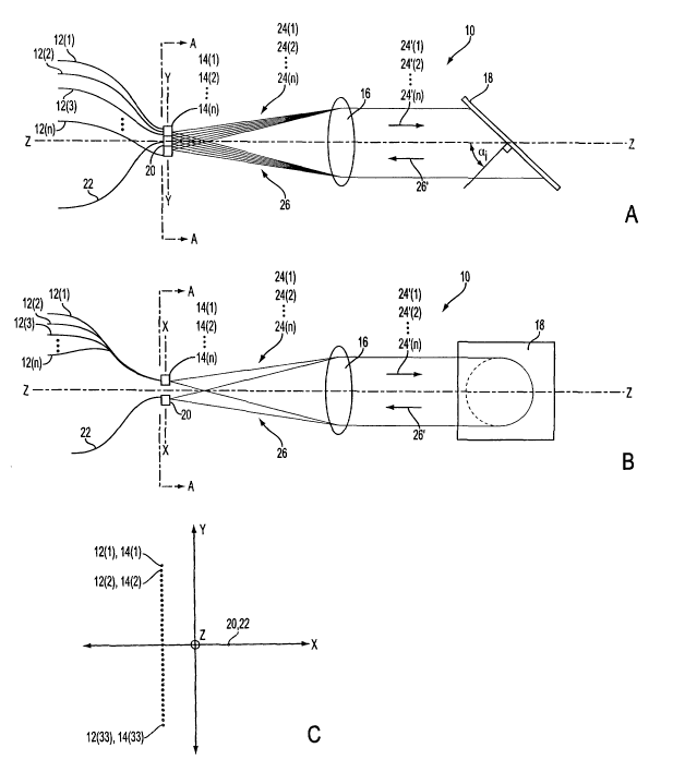
Figure la is a side view of a preferred embodiment of a
wavelength division multiplexing device employing patterned
IS optical components in accordance with the present invention.
Figure 1b is a top view of the wavelength division
multiplexing device shown in Figure la.
Figure lc is an end view of the optical fibers and the
corresponding patterned optical components, along section A-A
of Figures la and 1b.
17
CA 02405823 2002-10-09
WO 01/77725 PCT/USO1/11673
Figure 2a is a perspective view of a coupling device
containing a plurality of laser diodes for replacing the
plurality of optical input fibers in the multiplexing device
shown in Figures la and 1b.
Figure 2b is a perspective view of a coupling device
containing- a plurality of photodetectors for replacing the
plurality of optical fibers in the demultiplexing device shown
in Figures 3a and 3b.
Figure 3a is a side view of a preferred embodiment of a
wavelength division demultiplexing device employing patterned
optical components in accordance with the present invention.
Figure 3b is a top view of the wavelength division
demultiplexing device shown in Figure 3a.
Figure 4a is side view of a first embodiment of one of
the plurality of patterned optical input components shown in
Figure 1.
Figure 4b is a side view of a first embodiment of the
patterned optical output component shown in Figures la and 1b.
Figure 5a is a side view of a bi-convex
collimatingjfocusing microlens having a pure convex surface on
one side and a patterned phase mask canvex surface on the
opposite side in accordance with the present invention.
18
CA 02405823 2002-10-09
WO 01/77725 PCT/USO1/11673
Figure 5b is a side view of a plarlo-convex
colt imating/focusing microlens having a pure planar surface on
one side and a patterned phase mask convex surface on the
opposite side in accordance with the present invention.
Figure 6 is a front view of a substrate having an array
of patterned and non-patterned microlenses formed therein in
accordance with the present invention.
Figure 7 is a plot of the gaussian-shaped passband
profile of the improved wavelength division demultiplexing
device of Figures 3a and 3b that is widened as a result of the
use of non-phase masked microlenses.
Figure 8 is a plot of the profile of a cosinusoidal
patterned phase mask in accordance with the present invention.
Figure 9 is a plot of the passband profile of the
improved wavelength division demultiplexing device of Figures
3a and 3b that is flattened as a result of the use of
cosinusoidal patterned phase mask microlenses in accordance
with the present invention.
Figure 10a indicates how the periodic wavefront profiles
that are formed from the cosinusoidal patterned phase mask
microlenses described in Figure 8 are constructively added to
each other when they are completely in phase on center
19
CA 02405823 2002-10-09
WO 01/77725 PCT/USO1/11673
channel, thereby diffracting the maximum amount of en°rgy out
of the receiving fiber core, in accordance with the present
invention.
Figure lOb indicates how the periodic wavefront profiles
that are formed from the cosinusoidal patterned phase mask
microlenses described in Figure 8 are destructively canceled
when they are 180 degrees out of phase off center channel in
accordance with the present invention.
Figure 11 shows a plot of the widened gaussian-shaped
passband profile shun. in Figure 7 in comparison to a plot of
,~:
the widened and flattened passband profile shown in Figure 9.
Figure 12 is a plot of the profile of a chirped patterned
phase mask in accordance with the present invention.
Figure 13 is a plot of the passband profile of the
improved wavelength division demultiplexing device of Figures
3a and 3b that is flattened as a result of the use of chirped
patterned phase mask microlenses in accordance with the
present invention.
DETAILED DESCRIPTION OF EXEMPLARY EMBODIMENTS)
Referring to Figures la and 1b, there are shown a side
view and a top view, respectively, of a preferred embodiment
CA 02405823 2002-10-09
WO 01/77725 PCT/USO1/11673
o' a wavelength division multiplexing device 10 employing
patterned optical components in accordance with the present
invention. The multiplexing device 10 comprises a plurality
of optical input fibers 12, a corresponding plurality of
patterned optical input components 14, a collimating~focusing
lens 16, a reflective diffraction grating 18, a patterned
optical output component 20, and a corresponding optical
output fiber 22. All of the above-identified components of
the multiplexing device 10 are disposed along an optical axis
Z-2 of the multiplexing device 10, as will be described in
more detail below.
At this point it should be noted that the optical input
fibers 12 and the optical output fibers 22, as well as any
other optical fibers described herein, are single mode optical
fibers. Of course, however, this does not limit the present
invention to use with only single mode optical fibers. For
example, the present invention can also be used with multimode
optical ffibers.
The plurality of optical input fibers 12, as well as the
corresponding plurality of patterned optical input components
14, are arranged into one-dimensional input arrays {e.g., 1 x
33 arrays). The patterned optical output component 20, as
22
CA 02405823 2002-10-09
WO 01/77725 PCT/USO1/11673
well as the corresponding optical output fiber 22, are also
arranged into one-dimensional output arrays (i.e., 1 x 1
arrays?. For ease of alignment, each of the plurality of
patterned optical input components 14 may be secured to the
end of a corresponding one of the plurality of optical input
fibers 12,. but the present invention is not limited in this
regard. For example, each of the plurality of patterned
optical input components 14 may be aligned with, but separated
from, the .end of a corresponding one of the plurality of
optical input fibers 12. Similarly, for ease of alignment,
the patterned optical output component 20 may be secured to
the end of the corresponding optical output fiber 22, but the
present invention is not limited in this regard. For example,
the patterned optical output component 20 may be aligned with,
but separated from, the end of the corresponding optical
output fiber 22. For purposes of ease of optical fiber
handling and precision placement, both the plurality of
optical input fibers 12 and the optical output fiber 22 may be
secured within, for example, silicon V-groove assemblies.
w Referring to Figure Ic, there is shown an end view of the
plurality of optical input fibers 12, as well as the
corresponding plurality of patterned optical input components
22
CA 02405823 2002-10-09
WO 01/77725 PCT/USO1/11673
14, along section A-A of Figures la and 1b. Each of the
plurality of optical input fibers 12 is aligned with a
corresponding one of the plurality of patterned optical input
components 14. Both the plurality of optical input fibers 12
and the corresponding plurality of patterned optical input
components. l4 are arranged as 1 x 33 arrays.
Also referring to Figure lc, there is shown an end view
of the patterned optical output component 20, as well as the
corresponding optical output fiber 22, along section A-A of
Figures la and 1b. The patterned optical output component 20
is aligned with the corresponding optical output fiber 22.
Both the patterned optical output component 20 and the
corresponding optical output fiber 22 are arranged as 1 x 1
arrays.
Returning to Figures la and 1b, each of the plurality of
optical input fibers 12 transmits a single, monochromatic
optical input beam 24, while the optical output fiber 22
receives a single, multiplexed, polychromatic optical output
beam 26. Each of the monochromatic optical input beams 24
being transmitted from the plurality of optical input fibers
12 is carrying a single channel of data at a unique
wavelength, which is preferably, but not required to be,
23
CA 02405823 2002-10-09
WO 01/77725 PCT/USO1/11673
within the infrared (IR) region of the electromagne~.ic
spectrum. The single channel of data that is being carried by
each monochromatic optical input beam 24 is superimposed on
each corresponding unique wavelength by means (e. g., laser
diodes connected to the plural ity of optical input f fibers 12 ) ,
which are not shown here and which do not form a part of this
invention, but are well' known in the art. The unique
wavelengths of the monochromatic optical input beams 24 are
appropriately preselected such that the data channels
generally do not erfere with each other (i.a., there is
sufficient channel spacing), and the optical transmission
losses through both the optical input fibers 12 and the
optical output fiber 22 are low, as is also well known in the
art.
The multiplexed, polychromatic optical output beam 26
being received by the optical output fiber 22 is carrying a
plurality of channels of data at the unique wavelengths of
corresponding ones of the plurality of monochromatic optical
input beams 24. That is, the multiplexed, polychromatic
optical output beam 26 is carrying a plurality of channels of
data (e.g., 33 channels of data) at the unique wavelengths of
the monochromatic optical input beams 24 that are transmitted
24
CA 02405823 2002-10-09
WO 01/77725 PCT/USO1/11673
from the optical input fibers 12. The plurality of
monochromatic optical input beams 24 are combined into the
multiplexed, polychromatic optical output beam 26 through the
combined operation of the collimating/focusing lens 16 and the
S reflective diffraction grating 18, as will be described in
more detail below.
At this point it should be noted that the plurality of
optical input fibers 12 (as well as the corresponctlng
plurality of patterned optical input components 14) and the
patterned optical output component 20 (as well as the
corresponding optical output fiber 22) are disposed offset
from, but symmetrically about, the optical axis Z-Z of the
multiplexing device 10 so as to insure that the multiplexed,
polychromatic optical output beam 26 is directed to the
patterr_ed optical output component 20 and the corresponding
optical output fiber 22, and not to anywhere else. This
offset spacing of the plurality of optical input fibers 12 (as
well as the corresponding plurality of patterned optical input
components 14) and the patterned optical output component 20
(as well as the corresponding optical output fiber 22) is
determined based upon the focusing power of the
collimating/focusing lens 16, as well as the characteristics
2S
CA 02405823 2002-10-09
WO 01/77725 PCT/USO1/11673
of the diffraction grating 18 and the wavelengths of each of
the monochromatic optical input beams 24.
Each of the plurality of monochromatic optical input
beams 24 is transmitted from its corresponding optical input
fiber 12 through a corresponding one of the plurality of
patterned optical input components 14 and into the air space
between the plurality of patterned optical input components 14
and the collimating/focusing lens 16. Within this air space,
the plurality of monochromatic optical input beams 24 expand
in diameter until they become incident upon the
collimating/focusing lens 16. The collimating/focusing lens
16 collimates each of the plurality of monochromatic optical
input beams 24, and then transmits each collimated,
monochromatic optical input beam 24' to the reflective
diffraction grating 18.
At this point it should be noted that the optical axis of
the collimating/focusing lens 16 coincides with the optical
axis ~-Z of the multiplexing device 10 so as to insure that
the multiplexed, polychromatic optical output beam 26 is
directed to the patterned optical output component 20 and the
corresponding optical output fiber 22, and not to anywhere
else, as will be described in more detail below.
26
CA 02405823 2002-10-09
WO 01/77725 PCT/USO1/11673
The reflective diffraction grating 18 operates to
angularly disperse the plurality of collimated, monochromatic
optical input beams 24' by an amount that is dependent upon
the wavelength of each of the plurality of collimated,
monochromatic optical input beams 24'. Also, the reflective
diffraction grating 18 is oriented at a special angle (i.e.,
the Littrow diffraction angle, ai) relative to the optical
axis Z-Z of the multiplexing device 10 in order to obtain the
Littrow diffraction condition for an optical beam having a
wavelength that lies within or near the wavelength range of
the plurality of collimated, monochromatic optical input beams
24'. The Littrow diffraction condition requires that an
optical beam be incident on and reflected back from a
reflective diffraction grating at the exact same angle.
Therefore, it will be readily apparent to one skilled in the
art that the reflective diffraction grating 18 is used to
obtain near-Littrow diffraction for each of the plurality of
collimated, monochromatic optical input beams 24'
The Littrow diffraction angle, ai, is determined by the
well-known diffraction grating equation,
m1~ = 2d(sin ai)
27
CA 02405823 2002-10-09
WO 01/77725 PCT/USO1/11673
wherein m is the diffraction order, ~ is the wavelength, d is
the diffraction grating groove spacing, and ai is the common
angle of incidence and reflection. It will be readily
apparent to one skilled in the art that the Littrow
S diffraction angle, ai, depends upon numerous variables, which
may be varied as necessary to optimize the performance of the
multiplexing device 10. For example, variables affecting the
Littrow diffraction angle, ai, include the desired grating
diffraction order, the grating line pitch, and the wavelength
range of the multiexing device 10, among others.
At this point it should be noted that the reflective
diffraction grating 18 can be formed from a variety of
materials and by a variety of techniques. For example, the
reflective diffraction grating 18 can be formed by a three-
dimensional hologram in a polymer medium, or by replicating a
mechanically ruled master with a polymer material. In both
cases, the polymer is preferably overcoated with a thin,
highly reflective metal layer such as, for example, gold or
aluminum. Alternatively, the reflective diffraction grating
18 can be formed by chemically etching into a planar material
such as, for example, glass or silicon, which is also
28
CA 02405823 2002-10-09
WO 01/77725 PCT/USO1/11673
preferably overcoated with a thin, highly reflective metal
layer such as, for example, gold or aluminum.
As previously mentioned, the reflective diffraction
grating 18 operates to angularly disperse the plurality of
S collimated, monochromatic optical input beams 24'. Thus, the
reflective. diffraction grating 18 removes the angular
separation of the plurality of collimated, monochromatic
optical input beams 24', and reflects a collimated,
polychromatic optical output beam 26' back towards the
collimating/focusing lens 16. The collimated, polychromatic
optical output beam 26' contains each of the unique
wavelengths of the plurality of collimated, monochromatic
optical input beams 24'. Thus, the collimated, polychromatic
optical output beam 26' is a collimated, multiplexed,
polychromatic optical output beam 26'. The
collimating/tocusing lens 16 focuses the collimated,
multiplexed, polychromatic optical output beam 26'. The
resulting multiplexed, polychromatic optical output beam 26 is
transmitted from the collimatingifocusing lens 16 through the
patterned optical output component 20 ~ and into the
corresponding optical output fiber 22 for transmission
therethrough.
29
CA 02405823 2002-10-09
WO 01/77725 PCT/USO1/11673
At this point it should be noted that the plurality of
optical input fibers I2 could be replaced in the multiplexing
device 10 by a corresponding plurality of laser diodes 28
secured within a coupling device 30, such as shown in Figure
2a (although Figure 2a shows only a single 1 x 4 array). The
coupling device 30 serves to precisely group the plurality of
laser diodes 28 into a one-dimensional input array. The
plurality of laser diodes 28 are used in place of the
plurality of optical input fibers 12 to transmit the plurality
of monochromatic optical input beams 24 to the multiplexing
device 10. The array of laser diodes 28, as well as true
plurality of optical input fibers 12, may operate alone, or
may be used with appropriate focusing lenses (not shown) to
provide the best coupling and the lowest amount of signal loss
and channel crosstalk.
At this point it should be noted that the multiplexing
device 10, as well as all of the multiplexing devices
described herein, may be operated in a converse configuration
as a demultiplexing device 40, such as shown in Figures 3a and
~3b. The demultiplexing device 40 is physically identical to
the multiplexing device 10, and is therefore numerically
identified as such. However, the demultiplexing device 40 is
CA 02405823 2002-10-09
WO 01/77725 PCT/USO1/11673
functionally opposite to the mul tiplexing device 10. That is,
a multiplexed, polychromatic optical input beam 42 is
transmitted from the optical fiber 22, and a plurality of
monochromatic optical output beams 44 are transmitted to the
S plurality of optical fibers 12, wherein each one of the
plurality -of monochromatic optical output beams 44 is
transmitted to a corresponding one of the plurality of optical
fibers 12. The multiplexed, polychromatic optical input beam
42 is simultaneously carrying a plurality of channels of data,
each at a unique wavelength which is preferably, but not
required to be, within the infrared (IR) region of the
electromagnetic spectrum. The plurality of monochromatic
optical output beams 44~are each carrying a single channel of
data at a corresponding one of the unique wavelengths of the
multiplexed, polychromatic optical input beam 42. The
multiplexed, polychromatic optical input beam 42 is separated
into the plurality of monochromatic optical output beams 44
through the combined operation of the collimatingjfocusing
lens 16 and the reflective diffraction grating I8. Thus, the
~collimatingjfocusing lens 16 and the reflective diffraction
grating 18 operate to perform a demultiplexing function.
31
CA 02405823 2002-10-09
WO 01/77725 PCT/USO1/11673
At this point it should be noted that the plurality of
optical fibers 12 could be replaced in the demultiplexing
device 40 by a corresponding plurality of photodetectors 48
secured within a coupling device 50, such as shown, in Figure
2b (although Figure 2b shows only a single 1 x 13 array). The
coupling device 50 serves to precisely group the plurality of
photodetectors 48 into a 'one-dimensional input array. The
plurality of photodetectors 48 are used in place of the
plurality of optical fibers 12 to receive the plurality of
monochromatic optil output beams 44 from the demultiplexing
~,~3~.
device 40. The array of photodetectors 48, as well as the
plurality of optical fibers 12, may operate alone, or may be
used with appropriate focusing lenses (not shown) to provide
the best coupling and the lowest amount of signal loss and
channel crosstalk.
At this point it is appropriate to describe in more
detail the plurality of patterned optical input components 14
and the patterned optical output component 20, and the
function thereof. Referring to Figure 4a, there is shown a
first embodiment of one of the plurality of patterned optical
input components Z4 comprising a collimating microlens 60 and
a first patterned phase mask 62. In the case of the
32
CA 02405823 2002-10-09
WO 01/77725 PCT/USO1/11673
multiplexing device 10, the monochromatic optical irput beam
24 is transmitted from the core 13 of a corresponding optical
input fiber 12 to the collimating microlens 60. During this
period, the monochromatic optical input beam 24 has a
generally spherical wavefront 64 and is expanding due to
gaussian beam diffraction.
The collimating microlens 60 collimates the monochromatic
optical input beam 24 and then transmits the monochromatic
optical input beam 24 to the first patterned phase mask 62.
During this period, the monochromatic optical input beam 24 is
still slightly expanding due to gaussian beam diffraction, but
the monochromatic optical input beam 24 has a generally planar
wavefront 66 due to the effect of the collimating microlens
60. Also, the collimating microlens 60 causes a widening of
1S tine gaussian-shaped passband profile of the multiplexing
device 10, as described in more detail below.
The first patterned phase mask 62 introduces a first
patterned phase delay into the monochromatic optical input
beam 24 and then transmits the monochromatic optical input
beam 24 to the collimating/focusing lens 16 (not shown).
During this period, the monochromatic optical input beam 24 is
still slightly expanding due to gaussian beam diffraction, but
33
CA 02405823 2002-10-09
WO 01/77725 PCT/USO1/11673
the monochromatic optical input beam 24 also has a first
patterned wavefront 68 due to the first patterned phase delay
that is introduced into the monochromatic optical input beam
24 by the first~patterned phase mask 62. In accordance with
the present invention, the first patterned wavefront 68, and
hence the. first patterned phase delay, contribute to a
flattening of the peak of the gaussian-shaped passband profile
of the multiplexing device 10, as described in more detail
below.
Referring to Figure 4b, there is shown a first embodiment
of the patterned optical output component 20 comprising a
focusing microlens 70 and a second patterned phase mask 72.
Again in the case of the multiplexing device 10, the
multiplexed, polychromatic optical output beam 26 is
transmitted from the collimating/focusing lens 16 (not shown)
to the second patterned phase mask 72. During this period,
the multiplexed, polychromatic optical output beam 26 is being
focused by the collimating/focusing lens 16 (not shown) . Also
during this period, the multiplexed, pol~rchromatic optical
-output beam 26 has a first patterned wavefror_t 68 due to the
first patterned phase delay that is introduced into the
monochromatic optical input beam 24 (as well as all other
34
CA 02405823 2002-10-09
WO 01/77725 PCT/USO1/11673
monochromatic optical input beams 24 that are combined into
the multiplexed, polychromatic optical output beam 26 through
the combined operation of the collimating/focusing lens 16 and
the reflective diffraction grating 18) by the first patterned
phase mask 62. °
The second patterned phase. mask 72 introduces a second
patterned phase delay into the multiplexed, polychromatic
optical output beam 26 and then transmits the multiplexed,
polychromatic optical output beam 26 to the focusing microlens
70. During this period, the multiplexed, polychromatic
optical output beam 26 is still being focused as a result of
the collimating/focusing Lens 16 (not shown?. Also during
this period, the second patterned phase delay that is
introduced into the multiplexed, polychromatic optical output
1.5 beam 26 by the second patterned phase mask 72 is added to the
first patterned phase delay that is introduced into the
monochromatic optical input beam 24 (as well as all other
monochromatic optical input beams 24 that are combined into
the multiplexed, polychromatic optical output beam 26 through
the combined operation of the collimating/focusing lens 16 and
the reflective diffraction grating 18) by the first patterned
phase mask 62. The addition of the second patterned phase
CA 02405823 2002-10-09
WO 01/77725 PCT/USO1/11673
delay to the first patterned phase delay is wavelength
dependent. That is, the second patterned phase mask 72 and
the first patterned phase mask 62 are designed such that the
addition of the second patterned phase delay to the first
patterned phase delay results in either constructive or
destructive interference in the multiplexed, polychromatic
optical output beam 26 depending upon the actual wavelength of
each communication channel signal in relatior_ to the expected
unique center wavelength of that communication channel. Thus,
during this perie~,~, the wavefront of the multiplexed,
~:
polychromatic optical output beam 26 may vary from a second
patterned wavefront 78 as a result of the second patterned
phase delay and the first patterned phase delay constructively
adding to each other when they are completely in phase, to a
generally planar wavefront 76 as a result of the second
patterned phase delay and the first patterned phase delay
destructively canceling each other when they are 180 degrees
out of phase. The constructive adding, or interference,
results in more diffracted energy (and thus a greater
reduction in the amount of total energy at selected locations
in the passband profile), while the destructive canceling, or
interference, results in less diffracted energy (and thus a
36
CA 02405823 2002-10-09
WO 01/77725 PCT/USO1/11673
lesser reduction in the amount of total energy at selected
locations in the passband profile). The actual wavelength of
each communication channel signal may drift off the expected
unique center wavelength of that communication channel for a
number of reasons, including, for example, temperature and
laser diode modulation. In this particular embodiment, the
second patterned phase mask 72 and the first patterned phase
mask 62 are designed so as to result in a flattening of the
peak of the gaussian-shaped passband profile of the
multiplexing device 10, as described in more detail below.
The focusing microlens 70 focuses the multiplexed,
polychromatic optical output beam 26 and then transmits the
multiplexed, polychromatic optical output beam 26 toward the
optical output fiber 22. During this period, the multiplexed,
1.5 polychromatic optical output beam 26 varies between a
generally spherical wavefront 77 and a converging patterned
wavefront 79 due to the effect of the focusing microlens 70 on
the multiplexed, polychromatic optical output beam 26. Also
during this period, certain portions of the multiplexed,
polychromatic optical output beam 26 are slightly more focused
on the core 23 of the optical output fiber 22 as a result of
the focusing microlens 70 and due to the above-described
37
CA 02405823 2002-10-09
WO 01/77725 PCT/USO1/11673
destructive interference (or lack of the above-described
constructive interference) on certain portions of the
multiplexed, polychromatic optical output beam 26, while
certain other portions of the multiplexed, polychromatic
optical output beam 26 are scattered due to the above-
described constructive interference. Thus, those portions of
the multiplexed, polychromatic optical output beam 26 that are
not scattered due to the above-described constructive
interference are more likely to be coupled into the core 23 of
the optical output fiber 22 for transmission therethrough.
At this point it should be noted that the focusing
microlens 70 causes a further Widening of the gaussian-shaped
passband profile of the multiplexing device 10. That is, the
combination of the effect of the collimating microlens 60 on
the monochromatic optical input beam 24 (as well as all other
monochromatic optical input beams 24 that are combined into
the multiplexed, polychromatic optical output beam 26 through
the combined operation of the collimating/focusing lens 16 and
the reflective diffraction grating 1B), and the effect of the
focusing microlens 70 on the multiplexed, polychromatic
optical output beam 26 causes an overall widening of the
38
CA 02405823 2002-10-09
WO 01/77725 PCT/USO1/11673
gaussian-shaped passband profile of the multiplexing device
.
At this point it should be noted that the first patterned
phase mask 62 may be integrated into the collimating microlens
5 60, and the second patterned phase mask 72 may be integrated
into the focusing microlens 70. For example, referring to
Figure 5a, there is shown a bi-convex collimating/focusing
microlens 80 having a pure convex surface 82 on one side and
a patterned phase mask convex surface 84 on the opposite side .
10 Alternatively, referring to Figure 5b, there is shown a plano-
convex collimating/focusing microlens 90 having a pure planar
surface 92 on one side and a patterned phase mask convex
surface 94 on the opposite side.
At this point it should be noted that other types of
microlenses may be used in accordance with the present
invention. For example, microlenses havzng concave or
diffractive optic imaging surfaces may be used in accordance
with the present invention, and patterned phase masks may be
formed on any of these imaging surfaces.
At this point it is appropriate to describe in more
detail the manner in which the first patterned phase mask 62
and the second patterned phase mask 72 operate to achieve a
39
CA 02405823 2002-10-09
WO 01/77725 PCT/USO1/11673
flattening of the peak of the gaussian-shaped passband profile
of the multiplexing device 10. First, it is preferred that
the microlenses 60 and 70 (and/or the combined microlens/phase
mask) be placed at the focus of the collimatingjfocusing lens
16 so that the phase mask is imaged back onto its own plane.
Hence, if .the monochromatic optical input beams 24 or the
multiplexed, polychromatic optical output beam 26 are not
truncated or aberrated by the optical system, the phase of the
initial wavefront is preserved as Fresnel diffraction terms
vanish.
Second, since the collimating/focusing lens 16 is
preferably of telecentric design, the wavefront of the
monochromatic optical input beams 24 or the multiplexed,
polychromatic optical output beam 26 returning from the
optical system only translates across the receiving microlens
aperture as the illumination wavelength varies over the
passband range (i.e., there is no tilt). Hence, the overlap
integral of the source and receiver amplitude distributions
can be reduced to an integral over spatial dimensions, without
-needing an integration over angle.
Third, the mathematical operation of the input microlens
aperture amplitude distribution translating over the receiving
CA 02405823 2002-10-09
WO 01/77725 PCT/USO1/11673
microlens aperture ari~plitude distributior_ is a cross-
correlation. With no phase mask, the amplitude distribution
is given by the gaussian mode field diameter multiplied by the
truncation due to the micro-lens physical aperture. Thus,
S let,
-[t~)z~a)~~
G(x, y) = gaussian amplitude distribution = a
wherein a is equal to 1/e (amplitude mode field radius), and
let,
R{x, y) ---- Rectangular Aperture Function = ~l:x, y S ~,0 otherwise
wherein L is equal to f (aperture width).
The amplitude distribution at the microlens with no phase
mask is,
A-Po (x~ Y) = G(x~ Y)R{x~ Y)
The amplitude distribution at the microlens with a phase
mask is,
a_ 1
CA 02405823 2002-10-09
WO 01/77725 PCT/USO1/11673
Apm (~~ ~) = G(X~ y)R(X~ y)~(X) = Apa (X~ y)P(X)
wherein P(x) never is greater than 1 or less than -I. Hence,
the amplitude and therefore coupled energy into the fiber is
never greater than the non-phase masked case for the same
gaussian profile and aperture.
Let the phase mask function be a coarse sinusoidal (or
cosinusoidal) transmission grating in the x direction:
-i~~~sin~2.5~r L,
P(x) = a
wherein cp is the amplitude o~ the phase profile (i.e., O.ln),
and L is the half-width of the aperture.
The sinusoidal phase function can be expanded into a
Jacobi series in order to determine the amplitude of each
diffracted order from the coarse phase grating mask. The
amplitude for the ntn diffracted order is given by an nth order
Hessel function coefficient. The energy coupled into the
receiving fiber is given by the 0th order.
e;.~.s;nt~> ~ Jo (r~) + 2J2 (~) cos(29) + 2J~ (~) cos(48)+. . .
+2i~Jl{)sin{8)+ J3{)sin{39)+...,
42
CA 02405823 2002-10-09
WO 01/77725 PCT/USO1/11673
wherein Jz is a Bessel function of order n. For c~ = O.ln, Jo
- 0.975, Jz = 0_155, JZ = 0.012, J3 = 0.00064, . . ..
The resultant amplitude distribution after the receiver
phase mask, as the wavelength is varied over the passband, can
be calculated by multiplying the source and receiver amplitude
profiles together with a lateral shift of the source on the
receiver corresponding to'the location within the passband.
A one-dimensional cross-correlation of Ap*(x,y)sou=c~ with
Ap (x,y) receiver computes the fiber coupling amplitude overlap
integral as a function of location in the passband (square
result to get energy):
L L/2
A(a~) = ! ~ APs (~~~')APx (x ~- u,Y)dY~ = AP ~'s (x~Y) ~ -APR (~~Y)
-L-Ll2
Letting the source and receiver phase masks be equal, and
retaining only the first order diffraction terms from the
series expansion, the resultant amplitude of the source
multiplied by the receiver, as the source is shifted by ~x is:
43
CA 02405823 2002-10-09
WO 01/77725 PCT/USO1/11673
~~~W7~Z~ ~~o~xa~~~~o~xi ~x~~)~[~0~~~'
2i ~ ,h C~) ~o ~~)Lsln(2 ~.$ x) + sin(2 L (x . ~,~))~
LL
2J i(~»~os(2 ~.s (2x + fix)) - ~os(~ 2.s (_ ox))»
_~ L L
Integrating t~~: above over x and y as a function of ax,
and squaring to give intensity, gives the passband for the
sinusoidal phase mask.
By increasing the spatial frequency at the edge of the
aperture and increasing the amplitude of the Dhase modulation
with respect to the center, steeper slopes in the rejection
region can also be obtained. Also, orienting the phase
grating at an angle with respect to the fiber array direction
will cause the unwanted diffraction orders to fall out-of-line
to the fiber array, potentially improving cross-talk
rejection. It should be noted, however, that the spatial
frequency component in the v-groove direction needs to be
equal to the nominal case. Further, placing phase masked
4 a_
CA 02405823 2002-10-09
WO 01/77725 PCT/USO1/11673
microlenses directly adjacent to non-phase masked microlenses
can ease manufacturing alignment and reduce part count
logistics . For example, referring to Figure 6, there is shown
a substrate 100 having an array of microlenses formed therein.
The array of microlenses is arranged into a first column 102
and a second column 104. The microlenses in the first column
102 have patterned phaselmasks formed therein/on, while the
microlenses in the second column 104 do not have patterned
phase mask formed therein/on. Thus, the substrate 100 can be
shifted such that the microlenses in either the first column
102 or the second column 104 are aligned with the plurality of
optical input fibers 12, as well as the corresponding
plurality of patterned optical input components 14, which are
arranged into one-dimensional input arrays (e.g., 1 x 33
arrays).
At this point it is appropriate to describe a specific
working example of the demultiplexing device 40 as described
above in Figure 3 that incorporates the present invention
passband profile reshaping concepts just described. Assume
that the demultiplexing device 40 proposes 100Ghz channel
spacing, which results in approximately 0.8 nanometers
separation between communication channels near a 1550
CA 02405823 2002-10-09
WO 01/77725 PCT/USO1/11673
manometer center wavelength. The combination of the
collimating/focusing lens 16 and the reflective diffraction
grating 18 creates a 55 micron focus spot spacing between the
communication channels at the focal plane of the
collimating/focusing lens 16. Standard optical fibers (SMF-
28) have a.gaussian 1/e-squared mode field diameter (MFD) of
10.6 microns at the end. of optical fiber 22. The optical
system of the multiplexing device 10 creates a 55 micron shift
of focus spot with a 0.8 manometer change of incident
I0. wavelength. As a result of the small ratio of 10.6 micron MFD
out of 55 micron spacing, there are large gaps in coupling
between communication channels and the region over which
coupling is high is quite narrow. As described above, the
shape of the coupling with respect to wavelength is called the
passband.
Using non-phase masked microlenses (i.e., using no
patterned phase masks either separate from or integrated with
the microlenses) in front of both the optical fibers 12 and
the optical fiber 22, the diameter of each of the plurality of
-monochromatic optical output beams 44 can be optically re-
formed to a larger size. For example, the full angle
divergence in radians of a gaussian beam is given by:
a6
CA 02405823 2002-10-09
WO 01/77725 PCT/USO1/11673
8- ~~ a
wherein A is equal to waveler_gth and d is equal to MFD~iDer.
For a microlens focal length of 200 microns, a larger apparent
mode field diameter of 37 microns can be produced as follows:
4 1.55
MFD= 8~ f =-~ 200= 37
10.~
The gaussian-shaped passband profile that is widened as a
result of the above-described use of non-phase masked
microlenses is shown in Figure 7. The widened gaussian-shaped
passband profile shown in Figure 7 has the characteristics of
Passband (1dB down): 0.25nm, 31 GHz
Adjacent Channel Isolation at 1 dB down point: -3&.5 dB
In accordance with the present invention, a patterned
phase mask is formed on/in (or added in series with) the
microlenses so as to flatten the peak of the gaussian-shaped
passband profile of the demultiplexing device 40. For
example, a periodic patterned phase mask may be formed on/in
(or added in series with) the microlenses so as to flatten the
47
CA 02405823 2002-10-09
WO 01/77725 PCT/USO1/11673
peak of the gaussian-shaped passband profile of the
demultiplexing device 40. More specifically, a cosinusoidal
patterned phase mask having a period of 22 microns and
amplitude of O.ln is formed on/in (or added in series with)
S the microlenses. The profile of the cosinusoidal patterned
phase mask-is given by the following equation:
x
i~0_l:r~cos~ ~2~2n,
Phase(x) = a
and is shown in Figure 8, wherein arg is equal to:
O_l~c-cosC Z2~2~
The passband profile that is flattened as a result of the
above-described use of cosinusoidal patterned phase mask
microlenses is shown in Figure 9. The widened and flattened
passband profile shown in Figure 9 has the characteristics of
Passband (1dB down): 0.338nm, 42 GHz
Adjacent Channel Isolation at 1 dB down point: -29.7 dB
Referring to Figure 10a, the periodic wavefront profiles
that are formed from the cosinusoidal patterned phase mask
ag
CA 02405823 2002-10-09
WO 01/77725 PCT/USO1/11673
microlenses are shown constructively adding to each other when
they are completely in phase on center channel, thereby
diffracting the maximum amount of energy out of the receiving
fiber core. Referring to Figure 10b, the periodic wavefront
S profiles are shown destructively canceling each other when
they are 1.80 degrees out of phase off center channel. In this
scenario, the image of the'input phase pattern impinges out of
phase on the output phase pattern. When the amount of off-
center wavelength shift corresponds to a 180 degree shift of
the phase pattern profile, the patterns cancel, thereby
coupling all of the light into the receiving fiber core.
Referring to Figure 11, a plot of the widened gaussian-
shaped passband profile 106 as shown in Figure 7 is shown in
comparison to the widened and flattened passband profile 108
as sho:~m in Figure 9. As can be seen from this comparison'
the addition of the cosinusoidal patterned phase masks to the
microlenses also causes a steepening of the sideband slopes
due to energy loss in certain diffraction orders. The points
where the two plots intersect (identified by the X' s in Figure
'1l) are where the periodic wavefront profiles destructively
cancel each other when they are 180 degrees out of phase off
center channel.
49
CA 02405823 2002-10-09
WO 01/77725 PCT/USO1/11673
In accordance with the other aspects of the present
invention, a non-periodic patterned phase mask may
alternatively be formed on/in (or added in series with) the
microlenses so as to flatten the peak of the gaussian-shaped
passband profile of the demultiplexing device 40. More
specifically, a chirped patterned phase mask having increasing
amplitude and spatial frequency at the periphery may
alternatively be formed on/in (or added in series with) the
microlenses. The profile of the chirped patterned phase mask
is given by the following equation:
~~~ Lx-{1+~12,OOOx3')~
i-0-la 1+(~160z~) - sin ~~-~ -2n
Phase(x) = a
and is shown in Figure 12, wherein arg is equal to:
x-(1+I12,OOOx3')
O.l~r[1+(~160x~)~~- sin -2~r
27..~
The passband profile that is flattened as a result of the
above-described use of chirped patterned phase mask
microlenses is shown in Figure 13. The widened and flattened
passband profile shown in Figure 13 has the characteristics
of
SO
CA 02405823 2002-10-09
WO 01/77725 PCT/USO1/11673
Passband (1dB down): 0.316nm, 39.5 GHz
Adjacent Channel Isolation at 1dB down point: -35.8 dB
In view of the foregoing, it follows that there are many
variations of periodic (e. g., sinusoidal, cosinusoidal,
S triangular., square, etc.), modulated periodic (e. g.,
combinations of periodic functions having more than one
frequency), and nonperiodic (e. g., chirped, random, etc.)
patterns that can be formed oniin (or added in series with)
the microlenses in accordance with the present invention.
Also, the depth and width of the patterned phase masks can be
varied to control the amount of diffracted energy in
accordance with the present invention. Further, the patterned
phase masks may be designed in accordance with the present
invention so as to result in the reshaping of the passband
1S profiles of multiplexing devices in. other says than the
flattening of the peak of a gaussian-shaped passband profile
or the steepening of the sideband slopes of a gaussian-shaped
passband profile.
At this point it should be noted that it is within the
scope of the present invention to provide wavelength division
multiplexing/demultiplexing devices in accordance with the
51
CA 02405823 2002-10-09
WO 01/77725 PCT/USO1/11673
present invention using any or all of the concepts and/or
features described in U.S. Patent No. 5,999,672 (Attorney
Docket No. 34013-00005, Client Reference No. D-97031), issued
December 7, 1999; U.S. Patent No. 6,011,884 (Attorney Docket
No. 34013-00007, Client Reference No. D-97033), issued January
4,' 2000; U.S. Patent Application No. 09/257,045 (Attorney
Docket No. 34013-00008, Client Reference No. D-97031-CNT),
filed February 25, 1999; U.S. Patent Application No.
09/323,094 (Attorney Docket No. 34013-00010, Client Reference
No . D-99001) , filed:~June 1, 1999; U. S . Patent Application No.
,.
09/342,142 (Attorney Docket No. 34013-00011, Client Reference
No. D-99002) , filed June 29, 1999; U.S. Patent Application No.
09/382,492 (Attorney Docket No. 34013-00013, Client Reference
No. D-99004), filed August 25, 1999; U.S. Patent Application
No. 09/382,624 (Attorney Docket No. 34013-00014, Client
Reference No. D-99005), filed August 25, 1999; U.S. Patent
Application No. 09/363,041 (Attorney Docket No. 34013-00023,
Client Reference No. D-99014), filed July 29, 1999; U.S.
Patent Application No. 09j363,042 (Attorney Docket No. 34013-
00024, Client Reference No. D-99015), filed July 29, 1999;
U.S. Patent Application No. 09j392,670 (Attorney Docket No.
3407.3-00025, Client Reference No. D-99016) , filed September 8,
52
CA 02405823 2002-10-09
WO 01/77725 PCT/USO1/11673
1999; and U.S. Patent Application No. 09/392,831 (Attorney
Docket No. 3=X013-00026, Client Reference No. D-99017), filed
September 8 , 1999 ; all of which are hereby incorporated herein
by reference. For example, an wavelength division
multiplexing/demultiplexing device in accordance with the
present invention may be wholly or partially integrated, and
different types of lenses land lens configurations may be used.
In summary, the present invention comprises patterned
phase masks that are farmed in/on or added in series with
microlenses that are attached or disposed adj acent to the ends
of optical fibers in wavelength division
multiplexing/demultiplexing devices. In any case, the
patterned phase masks are preferably placed at~the focus of
the main collimating/focusing lens of the wavelength division
multiplexing/demultiplexing device.
' The microlenses are used to widen a gaussian-shaped
passband profile. The patterned phase masks cause energy to
be diffracted in certain locations within the passband
profile, thereby selectively reducing the amount of energy
that is coupled into the core of the receiving optical fiber.
That is, at certain locations within the passband profile, the
patterned phase masks cause either constructive or destructive
~5 3
CA 02405823 2002-10-09
WO 01/77725 PCT/USO1/11673
interference to occur as incident wavelength varies over the
passband profile. The constructive interference results in
more diffracted energy (and thus a greater reduction in the
amount of total energy at selected locations in the passband
profile), while the destructive interference results in less
diffracted. energy (and thus a lesser reduction in the amount
of total energy at selected locations in the passband
profile) . Also, the depth anal width of the patterned phase
masks can be varied to control the amount of diffracted
energy.
In the specific exe~iplary embodiment described herein,
constructive interference is used to reduce the transmitted
energy efficiency at the center and edges of the passband
profile, thereby flattening the peak of a gaussian-shaped
passband profile and steepening the sideband slopes of a
gaussian-shaped passband profile. That is, energy is
discarded at the center and edges of the gaussian-shaped
passband profile with respect to the shoulders of the desired
passband shape . The amount of energy that is discarded at the
center of the passband profile is tailored to match the
inverse of the peak of the gaussian-shaped passband profile.
Despite the particular application and results described
54
CA 02405823 2002-10-09
WO 01/77725 PCT/USO1/11673
above, the overall advantage of the present invention is the
ability to vary the amount of the effect over the width of the
passband profile.
The present invention is not to be limited in scope by
the specific embodiments described herein. Indeed, various
modifications of the present invention, in addition to those
described herein, will be apparent to those of ordinary skill
in the art from the foregoing description and accompanying
drawings. Thus, such modifications are intended to fall
within the scope of the following appended claims. Further,
although the present invention has been described herein in
the context of a particular implementation in a particular
environment for a particular purpose, those of ordinary skill
in the art will recognize that its usefulness is not limited
thereto and that the present invention can be beneficially
implemented in any number of environments for any number of
purposes. Accordingly, the claims set forth below should be
construed in view of the full bxeath and spirit of the present
invention as disclosed herein.