Language selection

Search

Patent 2405859 Summary

Third-party information liability

Some of the information on this Web page has been provided by external sources. The Government of Canada is not responsible for the accuracy, reliability or currency of the information supplied by external sources. Users wishing to rely upon this information should consult directly with the source of the information. Content provided by external sources is not subject to official languages, privacy and accessibility requirements.

Claims and Abstract availability

Any discrepancies in the text and image of the Claims and Abstract are due to differing posting times. Text of the Claims and Abstract are posted:

  • At the time the application is open to public inspection;
  • At the time of issue of the patent (grant).
(12) Patent Application: (11) CA 2405859
(54) English Title: TOP ILLUMINATED OPTO-ELECTRONIC DEVICES INTEGRATED WITH MICRO-OPTICS AND ELECTRONIC INTEGRATED CIRCUITS
(54) French Title: DISPOSITIFS OPTOELECTRONIQUES A ECLAIRAGE VERTICAL COMPORTANT DES CIRCUITS INTEGRES MICRO-OPTIQUES ET ELECTRONIQUES
Status: Dead
Bibliographic Data
(51) International Patent Classification (IPC):
  • H01S 5/026 (2006.01)
  • H01L 27/15 (2006.01)
  • H01L 31/00 (2006.01)
  • H01S 5/02 (2006.01)
  • H01S 5/183 (2006.01)
  • H01S 5/40 (2006.01)
  • H01S 5/00 (2006.01)
  • H01S 5/022 (2006.01)
(72) Inventors :
  • LIU, YUE (United States of America)
(73) Owners :
  • FINISAR CORPORATION (United States of America)
(71) Applicants :
  • HONEYWELL INTERNATIONAL, INC. (United States of America)
(74) Agent: RIDOUT & MAYBEE LLP
(74) Associate agent:
(45) Issued:
(86) PCT Filing Date: 2001-04-12
(87) Open to Public Inspection: 2001-10-25
Examination requested: 2004-08-05
Availability of licence: N/A
(25) Language of filing: English

Patent Cooperation Treaty (PCT): Yes
(86) PCT Filing Number: PCT/US2001/011996
(87) International Publication Number: WO2001/080285
(85) National Entry: 2002-10-11

(30) Application Priority Data:
Application No. Country/Territory Date
09/547,538 United States of America 2000-04-12

Abstracts

English Abstract


An opto-electronic integrated circuit device includes top emitter/detector
devices on a substrate. The top emitter/detector devices have top and bottom
sides. The top emitter/detector devices are capable of emitting and detecting
light beam from the top side, and have contact pads on this side. An optically
transparent superstrate is attached to the top side. Micro-optic devices such
as lenses can be attached to the superstrate. The contact pads are attached to
matching pads of an integrated circuit chip to produce an opto-electronic
integrated circuit.


French Abstract

Un dispositif à circuit intégré optoélectronique comprend des dispositifs d'émetteur/récepteur supérieurs situés sur un substrat. Les dispositifs supérieurs d'émetteur/détecteur comportent des côtés supérieur et latéraux, ils sont capables d'émettre et de détecter un faisceau de lumière depuis le côté supérieur et comprennent des plages de contact sur ce même côté. Une couche supérieure optiquement transparente est fixée au côté supérieur. Des dispositifs micro-optiques tels que des lentilles peuvent être fixés à la couche supérieure. Les plages de contact sont attachées à des plages adaptées d'un microcircuit intégré pour former un circuit intégré optoélectronique.

Claims

Note: Claims are shown in the official language in which they were submitted.


WHAT IS CLAIMED IS:
1. A method of packaging opto-electronic devices, comprising:
forming a top emitter/detector devices on a substrate, wherein the top
emitter/detector devices having top contact pads, wherein the top
emitter/detector devices
having a top side on the top contact pads and disposed across from the
substrate, and
wherein the substrate having a bottom side across from the top side;
attaching an optically transparent superstrate onto the top side of the top
emitter/detector devices such that the optically transparent superstrate has a
top surface
across from the top side of the substrate;
exposing the top contact pads to the bottom side;
forming bottom contact pads on the bottom side; and
connecting the bottom contact pads with the top contact pads.
2. The method of claim 1, wherein the top emitter and top detector devices
comprises
a plurality of top emitter/detector devices for an opto-electronic chip.
3. The method of claim 1, wherein the top emitter device is a vertical cavity
surface
emitting laser device capable of emitting light away from the substrate.
4. The method of claim 1, wherein the top detector device is a metal-
semiconductor-
metal photo detector.
5. The method of claim 1, wherein the top emitter/detector devices comprises
top
emitter/detector devices capable of emitting and detecting a light beam of 850
nanometers
wavelength respectively.
9


6. The method of claim 1, wherein the substrate is a wafer of gallium
arsenide.

7. The method of claim 6, further comprising testing the wafer of gallium
arsenide
substrate including the top emitter/detector devices to qualify after
fabricating the top
emitter/detector devices on the wafer of gallium arsenide substrate.

8. The method of claim 6, wherein the wafer of gallium arsenide substrate is
about 625
microns in thickness.

9. The method of claim 1, wherein the exposing the top contact pads to the
bottom
side further includes:
thinning the substrate from the bottom side to a predetermined thickness; and
forming via in the substrate from the thinned bottom side to expose the top
contact
pads to the bottom side.

10. The method of claim 9, wherein the forming via comprises chemically
etching the
bottom side of the thinned substrate to expose the top contact pads to the
bottom side.

11. The method of claim 9, wherein the forming via comprises mechanically
drilling
the bottom side of the thinned substrate to expose the top contact pads to the
bottom side.

12. The method of claim 9, wherein connecting bottom contact pads with the top
contact pads further includes forming a thru-the-via metal to connect the
bottom contact
pads with the top contact pads.

13. The method of claim 1, wherein the exposing the top contact pads to the
bottom
side further includes removing the substrate from the bottom side to expose
top contact
pads to the bottom side.

10


14. The method of claim 1, wherein the optically transparent superstrate is
made from
a material transparent to a light beam of 850 nanometers wavelength.

15. The method of claim 1, wherein the top emitter and top detector devices
and the
optically transparent superstrate have similar thermal properties to withstand
thermal
cycling used during a subsequent processing and packaging.

16. The method of claim 1, wherein the optically transparent superstrate is
made from
a wafer of sapphire.

17. The method of claim 1, wherein the optically transparent superstrate is
made from
a wafer of glass.

18. The method of claim 1, further comprising integrating micro-optic devices
on to the
top surface of the optically transparent superstrate to provide an optical
processing
capability to the top emitter and top detector devices.

19. The method of claim 18, wherein the optical processing comprises beam
shaping.

20. The method of claim 18, wherein the beam shaping includes beam focusing.

21. The method of claim 18, wherein the beam shaping includes beam filtering.

22. The method of claim 18, wherein the beam shaping includes beam tilting.

23. The method of claim 18, wherein the micro-optic devices comprises a wafer
of
micro optic devices.

11


24. The method of claim 23, further comprising bump bonding the bottom contact
pads
with matching pads of an integrated circuit device to produce an opto-
electronic integrated
circuit device having a having a high density optical I/O capability on an
integrated circuit
device.

25. A method of packaging an opto-electronic device having a high density
optical I/O
capability on an integrated circuit device, comprising:
forming a plurality of top emitter/detector devices having top contact pads on
a
wafer of gallium arsenide substrate, wherein the plurality of top
emitter/detector devices
having a top side on the top contact pads and disposed across from the wafer
of gallium
arsenide substrate, and wherein the substrate having a bottom side across from
the top side;
attaching a wafer of optically transparent superstrate onto the top side of
the
plurality of top emitter/detector devices such that the wafer of optically
transparent
superstrate having a top surface across from the top side;
exposing the top side contact pads to the bottom side of the wafer of
substrate;
forming bottom contact pads on to the bottom side of the wafer of substrate;
connecting the bottom contact pads with the top contact pads to form a
plurality of
opto-electronic devices;
integrating a wafer of micro-optic devices on to the top surface of the
optically
transparent superstrate such that the micro-optic devices provide an optical
processing
capability to the plurality of top emitter/detector devices;
dicing the plurality of opto-electronic devices including the micro-optic
devices to
produce opto-electronic chips; and
bump bonding the bottom contact pads of an opto-electronic chip with matching
pads of an integrated circuit device to produce an opto-electronic integrated
circuit device
having a having a high density optical I/O capability on an integrated circuit
device.

12


26. An opto-electronic device, comprising:
a substrate;
top emitter/detector devices, wherein the top emitter/detector devices are
formed
on to the substrate such that the top emitter/detector devices having a top
side, wherein the
top emitter/detector devices emits and detects light from the top side, and
wherein the
substrate having a bottom side across from the top side, wherein the top
emitter/detector
devices further having contact pads on the top side, wherein the bottom side
includes
bottom side contact pads, wherein the bottom side contact pads are connected
to the top
side contact pads to bring the top side contact pads to the bottom side; and
an optically transparent superstrate, attached to the top side of the top
emitter/detector devices such that the optically transparent substrate is
across from the
bottom side, wherein the optically transparent substrate having a top surface
across from
the top side.

27. The device of claim 26, wherein the top emitter/detector devices are a
plurality of
top emitter/detector devices.

28. The device of claim 26, wherein the top emitter device is a vertical
cavity surface
emitting laser device capable of emitting light away from the substrate.

29. The device of claim 26, wherein the top detector device is a metal-
semiconductor-
metal photo detector.

30. The device of claim 26, wherein the top emitter/detector devices are
capable of
emitting and detecting a light beam of 850 manometers wavelength.

31. The device of claim 26, wherein the substrate is a wafer of gallium
arsenide.

13


32. The device of claim 26, wherein the optically transparent superstrate is
made from
a material transparent to a light beam of 850 nanometers wavelength.

33. The device of claim 26, further includes micro-optic devices, wherein the
micro-
optic devices are attached to the top surface of the optically transparent
substrate such the
micro-optic devices are capable of processing a light beam.

34. The device of claim 26, wherein the top emitter/detector devices and the
optically
transparent superstrate have similar thermal properties.

35. The device of claim 26, wherein the optically transparent superstrate is
made from
sapphire.

36. The device of claim 26, wherein the optically transparent superstrate is
made from
glass.

37. The device of claim 26, further includes an integrated circuit device,
wherein the
bottom side contact pads are attached to the matching pads of the integrated
circuit device
to provide a high capacity optical I/O capability to the integrated circuit
device.

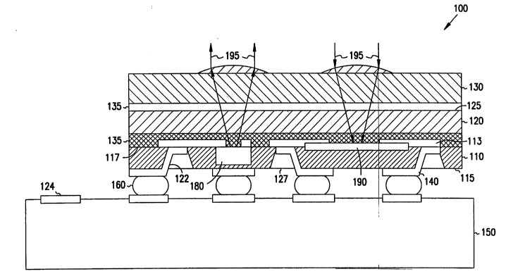
38. An opto-electronic integrated circuit device, comprising:
a substrate;
top emitter/detector devices, wherein the top emitter/detector devices are
formed
on to the substrate such that the top emitter/detector devices having a top
side, wherein the
top emitter/detector devices emits and detects light from the top side, and
wherein the
substrate having a bottom side across from the top side, wherein the top
emitter/detector
devices further having top contact pads on the top side, wherein the bottom
side includes

14


bottom side contact pads, wherein the bottom side contact pads are connected
to the top
side contact pads to bring the top side contact pads to the bottom side;
an optically transparent substrate, attached to the top side of the top
emitter/detector
devices such that the optically transparent substrate is across from the
bottom side, wherein
the optically transparent substrate having a top surface across from the top
side;
micro-optic devices, attached to the top surface of the optically transparent
substrate such that the micro-optic devices can provide optical processing to
the top
emitter/detector devices; and
an integrated circuit device, attached to the bottom side of the substrate
such that
the bottom contact pads are in contact with matching pads of the integrated
circuit device
to produce an integrated circuit device having a high capacity optical I/O.

39. The device of claim 38, wherein the top emitter/detector devices are a
plurality of
top emitter/detector devices.

40. The device of claim 38, wherein the top emitter device is a vertical
cavity surface
emitting laser device capable of emitting light away from the substrate.

41. The device of claim 38, wherein the top detector device is a metal-
semiconductor-
metal photo detector.

42. The device of claim 38, wherein the top emitter/detector devices are
capable of
emitting and detecting a light beam of 850 nanometers wavelength.

43. The device of claim 38, wherein the optically transparent superstrate is
made from
a material transparent to the light beam of 850 nanometers wavelength.

15


44. The device of claim 38, wherein the top emitter/detector devices and the
optically
transparent superstrate have similar thermal properties.

45. The device of claim 38, wherein the optically transparent superstrate is
made from
sapphire.

46. The device of claim 38, wherein the optically transparent superstrate is
made from
glass.

16

Description

Note: Descriptions are shown in the official language in which they were submitted.


CA 02405859 2002-10-11
WO 01/80285 PCT/USO1/11996
TOP ILLUMINATED OPTO-ELECTRONIC DEVICES INTEGRATED WITH
MICRO-OPTICS AND ELECTRONIC INTEGRATED CIRCUITS
Government Tnterest
This invention was made with United States Government support under contract
F5014-UCSD. The Government may have certain rights in the invention.
Back orb and of the Invention
Optical interconnect technology has been successfully implemented in long
distance
telecommunications, in local area network communication systems, in computer-
to-
computer, and board-to-board interconnections. The complexity and speed of
integrated
circuit devices such as microprocessors continue to increase at a very high
rate. However,
the input and output (I/O) capability of these devices has not been able to
scale at the same
rate, because of the existing limitations in electronic packaging of these
devices. Also, the
current technologies of integrating large arrays of opto-electronic devices
with integrated
circuit devices require bottom emitting/detecting of a light beam, and these
methodologies
are generally not scalable for a wafer-scale fabrication and/or integration of
both emitters
and detectors.
Therefore there is a need for a method of packaging an opto-electronic device
with
an integrated circuit device for a scalable wafer-scale fabrication, and at
the same time
providing a large-scale I/O capability to an integrated circuit device.
Summary of the Invention
These and other aspects, advantages, and features of the present invention
will be
set forth in part in the description which follows, and in part will become
apparent to those
skilled in the art by reference to the following description of the invention
and referenced
1


CA 02405859 2002-10-11
WO 01/80285 PCT/USO1/11996
drawings, or by practice of the invention. The aspects, advantages, and
features of the
invention are realized and attained by means of the instrumentalities,
procedures, and
combinations particularly pointed out in the appended claims and their
equivalents.
According to one aspect of the present subject matter, a method of packaging
an
opto-electronic integrated circuit device includes forming top
emitter/detector devices on
a substrate such that the top emitter/detector devices have top contact pads
on a top side of
the top emitter/detector devices, wherein the top side is disposed across from
the substrate,
and further the substrate has a bottom side that is across from the top side
of the top
emitter/detector devices. An optically transparent superstrate is attached
onto the top side
of the top emitter/detector devices such that the optically transparent
superstrate having a
top surface across from the top side of the top emitter/detector devices. The
top contact
pads are exposed on the bottom side of the substrate. The bottom contact pads
are formed
on the bottom side and the bottom contact pads are connected to the top
contact pads to
bring the top contact pads to the bottom side. The bottom side contact pads
are bonded
with matching pads of an integrated circuit device to form an opto-electronic
integrated
circuit device having a high density optical I/O on an integrated circuit
device.
Other aspects of the invention will be apparent on reading the following
detailed
description of the invention and viewing the drawings that form a part
thereof.
Brief Deseri~tion of the Drawings
In the drawings, like numerals describe substantially similar components
throughout the several views. Like numerals having different letter suffixes
represent
different instances of substantially similar components.
Figure 1 is a sectional view of one embodiment of the packaging technique of a
device packaged according to the invention.
Figure 2. is a flow diagram of an illustrative method of packaging a device
according to the invention.
2


CA 02405859 2002-10-11
WO 01/80285 PCT/USO1/11996
Detailed Description
In the following detailed description, reference is made to the accompanying
drawings which form a part hereof, and in which is shown by way of
illustration specific
embodiments in which the invention may be practiced. These embodiments are
described
in sufficient detail to enable those skilled in the art to practice the
invention. It is
understood that the embodiments may be combined, that other embodiments may be
utilized, and that structural, logical and electrical changes may be made
without departing
from the spirit and scope of the present invention. The following detailed
description is,
therefore, not to be taken in a limiting sense, and the scope of the present
invention is
defined by the appended claims and their equivalents.
In this document the term top emitter device is understood to refer to a
vertical
cavity surface emitting laser (VCSEL) or similar device that emits light away
from a
substrate, and the top detector device refers to a metal-semiconductor-metal
photodetector
(PD) or similar device. In this document, top side refers to a growing side of
the top
emitter/detector devices on a substrate, and bottom side refers to a side on
the substrate that
is across from the top side. Opto-electronic device refers to a substrate
including top
emitter/detector devices on a top side, and further including a transparent
superstrate on the
top emitter/detector devices. Top emitter/detector refers to devices emitting
and detecting
light from the top side of the top emitter/detector devices. The term
superstrate refers to a
wafer of optically transparent material disposed on a semiconductor substrate
including a
plurality of top emitter and top detector devices. Also, top surface refers to
a surface on the
transparent superstrate that is across from the top side, and bottom surface
is referred to the
exposed top emitter/detector devices and the bottom surface is also understood
to be
disposed across from the top surface.
Figure 1 is a front sectional view, illustrating generally, by way of example,
but not
by way of limitation, one embodiment of packaging an opto-electronic
integrated circuit
device 100 according to the present invention. This is accomplished in this
embodiment by
forming top emitter/detector devices on a thinned substrate 110 such that the
top
3


CA 02405859 2002-10-11
WO 01/80285 PCT/USO1/11996
emitter/detector devices have a top side 117 across from the thinned substrate
110. In this
embodiment the thinned substrate has a bottom side 115 across from the top
side 117. Top
emitter/detector devices I IO emit and detect Iight away from the thinned
substrate 110. Top
emitter/detector devices have top contact pads 113 on the top side 117. In one
embodiment
the thinned substrate is a wafer of gallium arsenide. In this embodiment the
wafer of
gallium arsenide includes plurality of top emitter/detector devices. The top
emitter device
is a vertical cavity surface emitting laser (VCSEL) device capable of emitting
light away
from a planar surface of the substrate, and the top detector device is a metal-
semiconductor-
metal photodetector device. In this embodiment, the top emitter/detector
devices on the
thinned substrate 110 are capable of emitting and detecting a light of 850
nanometers
wavelength.
An optically transparent superstrate 120 is attached to the top side I17 of
the top
emitter/detector devices on the thinned substrate 110 such that the optically
transparent
superstrate 120 is across from the bottom side 115. The optically transparent
superstrate has
a top surface 125 across from the top side 117. The optically transparent
superstrate 120 is
made from a wafer of sapphire in this example. In another embodiment, the
optically
transparent superstrate is a wafer of glass. In a further embodiment, the
materials of
optically transparent superstrate 120 and the top emitter/detector devices on
thinned
superstrate 110 have similar thermal properties so that they can withstand
rapid thermal
cycling introduced during subsequent processing and packaging. The optically
transparent
superstrate 120 can be bonded to the top emitter/detector devices 110. In this
embodiment
the bonding adhesive also has thermal properties similar to that of the
optically transparent
superstrate and the top emitter/detector devices. The optically transparent
superstrate 120
is transparent to a light of 850 nanometers wavelength. The thickness of the
optically
transparent superstrate 120 is sufficient to impart mechanical strength to the
thinned
substrate including the top emitter/detector devices 110.
The opto-electronic integrated circuit device 100 can further include micro-
optic
devices 130 attached to the top surface 125 of the optically transparent
superstrate 120. In
4


CA 02405859 2002-10-11
WO 01/80285 PCT/USO1/11996
this embodiment the micro-optic devices 130 are aligned with the top
emitter/detector
devices 110 to provide an optical processing capability to the top
emitter/detector devices
on the thinned substrate 110. In one embodiment the optical processing
includes beam
shaping for the top emitter/detector devices. 110.
The top side contact pads of the top emitter/detector devices 110 are brought
to the
bottom side contact pads by a through-the-via metal layer 122. An integrated
circuit device
150 is attached to the top emitter/detector devices 110. The bottom side
contact pads 140
of the top emitter/detector devices on the thinned substrate 110 can be bump
bonded, using
solder balls 160, to matching pads 124 of the integrated circuit device 150 to
provide a high
capacity optical I/O capability to the integrated circuit device 150.
Figure 2. is a flow diagram illustrating generally one embodiment of a method
200
of packaging an opto-electronic device having a high density I/O capability to
an electronic
integrated circuit device. Method 200 includes forming top emitter/detector
devices on a
top side of a substrate, block 210. In this embodiment, the top
emitter/detector devices have
top contact pads on the top side. The substrate includes a back side that is
across from the
top side. The top emitter/detector devices further includes an etch stop layer
on the top side.
The top emitter device includes a VCSEL capable of emitting light away from
the substrate,
and the top detector includes a metal-semiconductor-metal PD. Forming of the
top
emitter/detector devices on the substrate comprises forming 2-dimensional
arrays of
VCSEIJPD devices on a wafer, which can be of gallium arsenide. The top
emitter/detector
devices can have a pitch of 50 micrometers or less, and the wafer of gallium
arsenide can
be about 625 microns in thickness. The top emitter/detector devices on the
substrate can
be tested and qualified at this point if desired.
The next step 220 in the process is attaching an optically transparent
superstrate 120
onto the top side of the top emitter/detector devices such that the optically
transparent
superstrate has a top surface across from the top side of the substrate 220.
The optically
transparent superstrate can be made from a material transparent to the light
of 850
nanometers wavelength, such as sapphire or glass. The optically transparent
superstrate is


CA 02405859 2002-10-11
WO 01/80285 PCT/USO1/11996
of sufficient thickness to provide mechanical support to the exposed top
emitter/detector
devices. The optically transparent superstrate and the top emitter/detector
devices can be
made of materials having similar thermal properties, to withstand thermal
cycling
introduced during subsequent processing and packaging.
The next step 230 in the process is exposing the top contact pads to the
bottom side
240. This step can be achieved by thinning the substrate from the back side of
the substrate
such that the top contact pads are exposed to the bottom side. The thinning
step can also
include forming via in the substrate from the thinned bottom side to expose
the top contact
pads to the bottom side. A via can be formed by chemically etching the bottom
side of the
thinned substrate to the etch stop layer, to expose the top contact pads to
the bottom side.
Alternatively, the forming the via comprises mechanically drilling the bottom
side of the
thinned substrate to expose the top contact pads to the bottom side. Thinning
can be by
mechanically lapping the bottom side of the gallium arsenide substrate to a
thickness of
about 50 microns. The exposing step can also include removing the substrate to
expose the
top contact pads to the bottom side.
Step 240 in the process includes forming bottom contact pads on the bottom
side.
The next step 250 includes connecting the bottom contact pads with the top
contact pads
to bring the top contact pads to the bottom side to form an opto-electronic
device. This can
be done by plating the bottom contact pads to bring the top contact pads to
the bottom side.
Plating cn include forming through-the-via metal to bring the top contact pads
to the bottom
side. This has an advantage in that the back side contact pads and matching
pads of an
integrated circuit device would be in the same plane, making it easy to
further bond the
opto-electronic device to the integrated circuit device and to provide the
capability of
having a high density I/O to the integrated circuit device. Also, having the
back side contact
pads and matching pads of an integrated circuit device in the same plane
facilitates locating
the front side contact pads anywhere as needed, for example to avoid
interfering with the
location of the emitter/detector devices.
6


CA 02405859 2002-10-11
WO 01/80285 PCT/USO1/11996
Step 260 in the process involves integrating a wafer of micro-optic devices
130
onto the top surface of the optically transparent superstrate 120 such that
the micro-optic
devices are aligned with corresponding top emitter/detector devices 260 to
provide an
optical processing capability to them. Optical processing can include, for
example, beam
shaping, focusing a light beam, filtering the light beam, and tilting the
light beam.The wafer
of micro-optic devices can be fabricated on a separate substrate, then tested
and qualified
before integrating it onto the opto-electronic devices. The wafer of micro-
optic devices can
be bonded to the top surface of the optically transparent superstrate.
Step 270 in the process bonds the opto-electronic devices to the integrated
circuit.
This can include dicing the opto-electronic devices including the micro-optic
devices, to
produce opto-electronic chips. Then the back side contact pads of the opto-
electronic chips
are bump bonded with matching pads of an integrated circuit device to produce
an opto-
electronic integrated circuit device having a high density optical I/O on an
integrated circuit
device.
Conclusion
The above described method provides, among other things, an integrated circuit
device having a high I/O capacity in an optical domain. The high I/O capacity
is
accomplished by forming top emitter/detector devices on a top side of a
substrate, wherein
the substrate has a bottom side across from the top side. The top
emitter/detector devices
emit and detect light on the top side. The top emitter/detector have top
contact pads on the
top side. The top contact pads are brought to the back side by connecting the
top contact
pads with bottom contact pads. An optically transparent superstrate is
attached to the top
side of the top emitterldetector devices such that the optically transparent
superstrate is
across from the bottom side and the optically transparent superstrate has a
top surface
across from the top side forming an opto-electronic device. Micro-optic
devices can be
attached to the top surface of the transparent substrate such that the micro-
optic devices
provide optical processing capability. Then an integrated circuit device is
attached to the
bottom side of the substrate such that the bottom contact pads are in contact
with matching
7


CA 02405859 2002-10-11
WO 01/80285 PCT/USO1/11996
pads of the integrated circuit device to form an opto-electronic integrated
circuit device
having a high Il0 capacity.
It is to be understood that the above description is intended to be
illustrative, and
not restrictive. Many other embodiments will be apparent to those of skill in
the art upon
reviewing the above description. The scope of the invention should, therefore,
be
determined with reference to the appended claims, along with the full scope of
equivalents
to which such claims are entitled.
8

Representative Drawing
A single figure which represents the drawing illustrating the invention.
Administrative Status

For a clearer understanding of the status of the application/patent presented on this page, the site Disclaimer , as well as the definitions for Patent , Administrative Status , Maintenance Fee  and Payment History  should be consulted.

Administrative Status

Title Date
Forecasted Issue Date Unavailable
(86) PCT Filing Date 2001-04-12
(87) PCT Publication Date 2001-10-25
(85) National Entry 2002-10-11
Examination Requested 2004-08-05
Dead Application 2006-04-12

Abandonment History

Abandonment Date Reason Reinstatement Date
2005-04-12 FAILURE TO PAY APPLICATION MAINTENANCE FEE

Payment History

Fee Type Anniversary Year Due Date Amount Paid Paid Date
Registration of a document - section 124 $100.00 2002-10-11
Application Fee $300.00 2002-10-11
Registration of a document - section 124 $100.00 2003-02-10
Maintenance Fee - Application - New Act 2 2003-04-14 $100.00 2003-03-20
Maintenance Fee - Application - New Act 3 2004-04-12 $100.00 2004-03-18
Registration of a document - section 124 $100.00 2004-06-25
Request for Examination $800.00 2004-08-05
Owners on Record

Note: Records showing the ownership history in alphabetical order.

Current Owners on Record
FINISAR CORPORATION
Past Owners on Record
HONEYWELL INC.
HONEYWELL INTERNATIONAL, INC.
LIU, YUE
Past Owners that do not appear in the "Owners on Record" listing will appear in other documentation within the application.
Documents

To view selected files, please enter reCAPTCHA code :


To view images, click a link in the Document Description column. To download the documents, select one or more checkboxes in the first column and then click the "Download Selected in PDF format (Zip Archive)" or the "Download Selected as Single PDF" button.

List of published and non-published patent-specific documents on the CPD .

If you have any difficulty accessing content, you can call the Client Service Centre at 1-866-997-1936 or send them an e-mail at CIPO Client Service Centre.


Document
Description 
Date
(yyyy-mm-dd) 
Number of pages   Size of Image (KB) 
Abstract 2002-10-11 1 67
Claims 2002-10-11 8 280
Drawings 2002-10-11 2 63
Description 2002-10-11 8 402
Representative Drawing 2002-10-11 1 26
Cover Page 2003-01-30 1 50
Prosecution-Amendment 2004-08-05 1 34
Assignment 2002-10-11 3 92
Assignment 2002-11-29 2 111
PCT 2002-11-29 9 316
Correspondence 2003-01-29 1 24
Assignment 2003-02-10 5 159
Correspondence 2003-04-01 3 84
Assignment 2002-10-11 5 140
Assignment 2003-09-10 1 29
Correspondence 2004-06-25 2 67
Assignment 2004-06-25 35 1,451
Correspondence 2004-07-27 1 15
Correspondence 2004-07-27 1 18