Note: Descriptions are shown in the official language in which they were submitted.
CA 02406158 2002-10-17
WO 01/80795 PCT/AU00/00371
TRANSCUTANEOUS POWER OPTIMIZATION CIRCUIT FOR COCHLEAR
IMPLANT
A. Field of Invention
This invention pertains to an optimization circuit in a
cochlear implant system and more particularly to a circuit
which monitors one or more parameters within the implant
such as the internal power supply level and the compliance
of the stimulation signals applied by the implant. If an
undesirable condition is indicated by these parameters, the
circuit generates control signals to correct the condition
by adjusting the coupling between the internal and external
components of the system.
B. Description of the Prior Art
Certain patients suffer from a hearing disability in
the inner ear which cannot be satisfactorily assisted by
normal hearing aids. However, if the aural nerve is intact,
the patient may have some aural functions restored with a
cochlear implant system. A typical cochlear implant system
presently available includes an external component or
processor and an internal component often called the
implanted stimulator. The external component includes a
microphone for receiving ambient sounds and converting them
into electrical signals, a processor for processing said
electrical signals into encoded signals and a transmitter
transmitting said encoded signals to the interrial component.
The internal component includes a receiver receiving
the encoded signals, a decoder for decoding said signals
into stimulation signals and an electrode array including
both intracochlear electrodes extending into the patient's
1
SUBSTITUTE SHEET (RULE 26) ROIAU
CA 02406158 2002-10-17
WO 01/80795 PCT/AU00/00371
cochlear and optionally one or more extra-cochlear
electrodes. The stimulation signals are applied in the form
of pulses having.durations and waveshapes determined by the
processor.
Because the internal component of the cochlear implant
system is relatively small, it is not normally provided with
its own permanent power supply. Instead, the internal
component is energized transcutaneously by RF signals
received from the external component with the use of two
inductively coupled coils, one provided in the external
component and the other being provided within the internal
component. The external component sends data to the
internal component, by first encoding the data into the RF
signals and then transmitting it across the transcutaneous
link. The internal component decodes the data from the
received RF signals and also stores the received RF energy
in a capacitor to power its electronics. In order to achieve
efficient power transfer across the transcutaneous link,
both coils are tuned to resonate, at or close to the
operating frequency of the transmitter and are held in axial
alignment with the aid of a magnetic coupling.
The amount of energy being transferred to the internal
component depends mainly on the amount of inductive coupling
between the two coils as well as the resonance frequency of
the respective coils. The former is dependent on the
thickness of the tissue separating the two coils, which
thickness varies over the patient population. Hence, for
identical cochlear implant systems the efficiency of energy
transfer varies from one patient to another.
2
SUBSTITUTE SHEET (RULE 26) ROIAU
CA 02406158 2002-10-17
WO 01/80795 PCT/AU00/00371
The required amount of energy varies with the patient,
(due to the electrode-tissue interface impedance being
patient specific) the system programming, and the sound
environment. Therefore, every cochlear implant system must
be designed so that adequate power is delivered to the
internal component for all patients under all conditions.
Hence, there is an excess energy transfer across the link
for patients with relatively smaller separation between the
coils, or a low electrode-tissue interface impedance,
resulting in a shorter battery life, than optimally desired.
Attempts have been made by others to resolve this
problem but they have not been entirely satisfactory. For
example, U.S. Patent No. 5,603,726 discloses a multichannel
cochlear implant system in which the implantable section
generates signals to a wearable processor indicative of the
status of the implantable section, such as its power level
and stimulation voltages. The information is used by the
wearable processor to modify the characteristics of the
signals transmitted. More particularly, the implantable
section has an internal power supply capable of producing
several outputs having different nominal DC levels.
Additionally, the implantable section is also capable of
providing unipolar or bipolar stimulation pulses between
various intercochlear electrodes as well as an indifferent
electrode. A telemetry transmitter is used to send data to
the wearable processor, the data being indicative of the
voltage levels of the power supply outputs, the amplitudes
of the stimulation signals and other parameters. The
wearable processor uses the power level signals to adjust
3
SUBSTITUTE SHEET (RULE 26) ROIAU
CA 02406158 2002-10-17
WO 01/80795 PCT/AU00/00371
the amplitude (and therefore the power) of the RF signals
transmitted to the implantable section. However, this
approach is disadvantageous because it requires an RF
transmitter having a variable programmable amplitude, and
utilizes a fixed tuning of the transmit coil, therefore
making no attempt to modulate the voltage on the tank
capacitors to track the voltage required to maintain system
compliance. Obviously such a transmitter is expensive to
make and more complex then a standard RF transmitter having
a preset amplitude. Moreover, sending information from the
implantable section about the amplitude of the stimulation
pulses after these pulses have already been applied is
ineffective because, if one of these pulses is out of
compliance, the external section can do nothing about it,
except crank up the power to insure that future pulses are
compliant. However, merely cranking the power without any
further intelligence wastes energy.
Commonly assigned application S.N. 09/244,345 filed
February 4, 1999 entitled HIGH COMPLIANCE OUTPUT STAGE FOR A
TISSUE STIMULATOR, incorporated herein by reference,
describes a cochlear implant system wherein the generation
of stimulation pulses is monitored, (i.e. the compliance of
the stimulation generation circuit) and a voltage multiplier
is used if necessary to ensure that the stimulation pulses
are of the desired intensity. This application essentially
deals with a system of improving the internal power supply
in order to eliminate stimulation pulses, and as such, there
is no provision in this application for transmission of data
back to the external section.
4
SUBSTITUTE SHEET (RULE 26) ROIAU
CA 02406158 2002-10-17
WO 01/80795 PCT/AU00/00371
OBJECTIVES AND SUN,iMARY OF THE INVENTION
In view of the above disadvantages of the prior art, it
is an objective of the present invention to provide a power
control circuit for a cochlear implant which is constructed
and arranged to automatically and dynamically optimize the
power transferred to the internal component based on one or
more preselected criteria by adjusting an inductive coupling
therebetween.
A further objective is to provide a power control
circuit for a cochlear implant which is constructed and
arranged to automatically and dynamically regulate the
inductive coupling with the internal component thereof to
insure that power is not wasted, thereby increasing the life
of the external component battery.
A further objective is to provide a cochlear implant
system wherein the external and internal systems are coupled
inductively, wherein the voltage of the internal supply is
monitored and the frequency of this coupling is tuned to
obtain optimal power transfer using the voltage as a
feedback signal.
Yet another obj ective is to provide a cochlear implant
system wherein the compliance of the stimulation signals is
monitored and used as a feedback signal to optimize the
power transfer to the internal component.
Yet a further objective is to provide a cochlear
implant with a compliance monitor arranged and constructed
to sense a possible out of compliance condition before the
respective stimulation pulse is completed and to adjust the
5
SUBSTITUTE SHEET (RULE 26) ROIAU
CA 02406158 2002-10-17
WO 01/80795 PCT/AU00/00371
power transferred to the internal section in such a manner
that the out of compliance condition is averted.
Other objectives and advantages of the invention shall
become apparent from the following description.
Briefly, a cochlear implant system constructed in
accordance with this invention includes an external speech
processor and an implantable stimulator having electronic
circuitry, the two components being coupled to each other
inductively by respective coils. Each coil is part of a
tank circuit. The external speech processor transmits RF
signals through the coupling. The implantable stimulator
uses these signals for two purposes. First, the energy of
the signals is stored in a storage element such as a
capacitor and used to power the electronic circuitry.
Second, the signals are decoded and used to derive the
stimulation signals applied to the aural nerve.
In one embodiment of the invention, a parameter
indicative of the voltage of the storage element is
monitored and sent back to the speech processor via a
secondary channel. The external speech processor then
adjusts the frequency of its tank circuit to regulate the
power transferred to the internal component to optimize it.
Additionally, or alternatively, the compliance of the
stimulation signals is monitored and used as a feedback
signal to control the frequency of the tank circuit to
optimize power transfer to the internal component. This
adjustment can be done either based on statistical basis, or
in response to an individual and specific out of compliance
condition.
6
SUBSTITUTE SHEET (RULE 26) ROIAU
CA 02406158 2002-10-17
WO 01/80795 PCT/AU00/00371
BRIEF DESCRIPTION OF THE DRAWINGS
Figure 1 shows a schematic diagram of a cochlear system
constructed in accordance with the present invention;
Figure 2 shows a schematic diagram of the external
component of the cochlear system of Figure 1;
Figure 3 shows a schematic diagram of the internal
component of the cochlear system of Figure 1;
Figures 4A, 4B and 4C show the power control signals
transmitted from the internal to the external components
respectively to indicate the power level induced within the
internal component;
Figure 5A and 5B show flow charts for the operation of
internal and external components of Figures 1-3,
respectively; and
Figure 6 shows two sets of typical biphasic stimulation
signals ~.efined by the speech processor;
Figure 7 shows the current pulses required to produce
the stimulation pulses of Fig. 6; and
Figure 8 shows the corresponding waveforms across the
current source.
DETAILED DESCRIPTION OF THE INVENTION
Referring first to Figure 1, a cochlear implant system
10 constructed in accordance with this invention includes an
external component 12 and an internal component 14. The
external component includes a speech processor 12A and is
associated with a microphone 16 for sensing ambient sounds
and generating corresponding electrical signals. These
signals are sent to the speech processor 12A which processes
the signals and generates corresponding encoded signals.
7
SUBSTITUTE SHEET (RULE 26) ROIAU
CA 02406158 2002-10-17
WO 01/80795 PCT/AU00/00371
The encoded signals are provided to a transmitter (including
a transmit coil 20) for transmission to the internal
component 14.
The internal component 14 (which may also be referred
to as an implantable stimulator) receives the power and data
via a receive coil 22. The RF power signal is stored by a
power supply 24 (See Fig. 3) which provides power for the
internal component 14. The data signals control the
operation of the internal component 14 so as to generate the
required stimulation pulses which are applied to the
auditory nerve of the patient via an electrode array 28.
The structure of the external speech processor 12A is
shown in more detail in Fig. 2. First, the audio signals
received from microphone 16 are fed to a signal processor
30. This signal processor 30 maps the audio signals into
excitation signals in accordance with one or more mapping
algorithms stored in a map memory 31. These excitation.
signals are encoded by a digital data encoder 34. The
encoder data is combined with an RF signal in the data and
power transmitter 36, and passed to the transmit coil 20 via
a tuneable tank circuit 38.
In accordance with the present invention, encoded
telemetry data is received back from the internal component
14 via coil 20, and is decoded by telemetry decoder 52. The
decoder telemetry data is passed to the tuning adjuster and
power controller 40, which uses the telemetry data to
generate a tuning adjustment signal. The tuneable tank
circuit 38 adjusts the tuning of the transmit coil 20
according to the tuning adjustment signal as described in
8
SUBSTITUTE SHEET (RULE 26) ROIAU
CA 02406158 2002-10-17
WO 01/80795 PCT/AU00/00371
more detail below. This can be achieved, for example, by
using an electrically controlled variable capacitor in
conjunction with a series tuning capacitor, or by any of
various similar means known to the art. Power to the whole
system 10 is provided by a power supply 50 which typically
includes a battery.
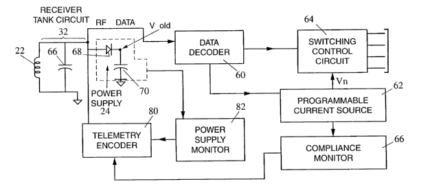
Referring now to Fig. 3, the internal component 14
includes a housing (not shown) which is hermetically sealed.
The component 14 also includes a receiver tank circuit 32
having the receive coil 22 and a capacitor 66. Signals
received through this tank circuit are fed to a power supply
24 generating an output voltage Vdd. The power supply is
represented in Fig. 3 by a diode 68 charging a capacitor 70.
The power supply 24 uses the energy of the received RF
signals to charge up the capacitor 70.
The RF signals are also fed to a data decoder 60. The
data decoder 60 derives from the RF signal the digital
excitation signals generated by the data encoder 34 and
generates corresponding stimulation control signals. These
signals are fed to a programmable current source 62 and a
switching control circuit 64. These two circuits cooperate
in response to the signals from data decoder 60 to apply the
cochlear stimulation signals to predetermined electrodes of
electrode array 28 in a known manner which is beyond the
scope of this invention.
Implant 14 further includes a compliance monitor 66
which generates an output that is fed to a telemetry encoder
80 as discussed more fully below; and a power supply monitor
82 which is used to monitor the voltage Vdd generated by
9
SUBSTITUTE SHEET (RULE 26) ROIAU
CA 02406158 2002-10-17
WO 01/80795 PCT/AU00/00371
power supply 24 and which provides a voltage condition
signal to telemetry encoder 80.
The compliance monitor 66 and power supply monitor 82
each sense certain specific functions of the internal
component and transmit them to the telemetry encoder 80.
The telemetry encoder 80 then transmits this information to
the telemetry decoder 52. The data is decoded and used to
adjust the power transmit between the coils, if necessary.
An exemplary mode of operation indicating the voltage
monitoring made is now described in conjunction with Figures
4A, B and C and 5A and 5B. At predetermined intervals, for
example, every 100ms, or alternatively after every
stimulation pulse, the telemetry encoder 80 generates a
first pulse F. (Step 100). This pulse may have a duration
of about lms. This pulse F indicates to the external speech
processor 12A that the implantable stimulator 14 is sending
data.
Next, the power supply monitor 82 compares the power
supply output voltage Vdd to a threshold value Vt and sends
the result to the telemetry encoder 80. More specifically,
starting with step 102, the power supply monitor 82 first
determines if Vdd>Vt. If it is, then in step 104, a
parameter pw (pulse width) is set to a predetermined value
A, of for example, 2ms by the telemetry encoder 80.
If in step 102 Vdd is not larger than Vt then in step
106 a check is performed to determine if Vdd is
approximately equal to Vt. If it is, then in step 108
parameter pw is set to zero. If it is not then, Vdd must be
SUBSTITUTE SHEET (RULE 26) ROIAU
CA 02406158 2002-10-17
WO 01/80795 PCT/AU00/00371
smaller than Vt and in step 110 the parameter pw is set to a
predetermined value B of, for example, lms.
Next, in step 112 a pulse D is generated having a pulse
width A or B, or no pulse is generated, depending on the
outcome of the decisions 102 and 106. The pulse D (if
present) is generated a period T after pulse F. T may be
about 1 ms. The results of this step are seen in Figures
4A, 4B, 4C.
For Figure 4A it has been determined that Vdd>Vt, and
hence pulse D with a pulse width A is sent about 1ms after
pulse F.
In Figure 4B, Vdd has been found to be about equal to
Vt and hence no pulse D is present.
In figure 4C, Vdd is found. to be smaller that Vt and
hence pulse D having a pulse width B is sent about 1 ms
after period F, pulse width B being generally shorter than
pulse width A. For example, pulse width A may be 2 ms and
pulse width B may be about 1 ms.
Pulse F and, if present, pulse D are then sent to the
tank circuit 32. As a result, a corresponding signal
appears on the transmit coil 20, which is then decoded by
the telemetry decoder 52.
The operation of the telemetry decoder 52 is now
described in conjunction with Fig. 5B. Starting with step
120, a pulse F is first detected which indicates that the
power supply monitor 82 is sending information about the
status of the power supply 24. Next in step 122 a check is
made to determine if a pulse D is present following pulse F.
11
SUBSTITUTE SHEET (RULE 26) ROIAU
CA 02406158 2002-10-17
WO 01/80795 PCT/AU00/00371
If this pulse is not detected, then in step 130 the previous
operations are continued with no change.
If in step 122, a pulse D is detected then in step 124
a determination is made as to whether this pulse D has a
pulse width A or a pulse width B. A telemetry pulse D
having a relatively long pulse width, in a range
corresponding to the pulse width A (for example if pulse D
exceeds 1.5 ms), indicates that the implant supply voltage
is high (i.e. Vdd> Vt). In step 126, the tuning adjuster
and power controller 40 therefore adjusts the tunable tank
circuit 38 to reduce the power transferred to the implant.
A preferred method to accomplish this effect is to reduce
the resonance frequency of the tank circuit.
If the telemetry pulse is less than l.5ms, (indicating
a pulse width B and that the power supply Vdd<Vt) then in
step 128 the tuning adjuster and power controller 40
adjusts the tunable tank circuit 38 to increase the
transferred power.
The tunable tank circuit 38 is adjusted by the tuning
adjuster and power controller 40 via means of a tuning
capacitor (not shown) which is preferably a voltage
dependent capacitor. It should be appreciated that the
tunable tank circuit 38 could also be tuned by other known
means as would be understood by one skilled in the art.
Similarly, the above mentioned operation may be
performed in respect of the compliance monitor signal, as
described in more detail below.
Briefly, referring to Fig. 3, under the control of
commands from data decoder 60, the programmable current
12
SUBSTITUTE SHEET (RULE 26) ROIAU
CA 02406158 2002-10-17
WO 01/80795 PCT/AU00/00371
source 62 generates current pulses which are applied to the
electrodes by switching control circuit 64. Figure 6
depicts two typical stimulation current waveforms 70 and 73
which may be requested by the signal processor 30. Tt can
be seen that each waveform is biphasic, consisting of two
current pulses of equal amplitude and opposite polarity.
Thus, lower amplitude biphasic current waveform 70 consists
of positive and negative pulses 71 and 72 respectively, and
higher amplitude current waveform 73 consists of positive
and negative pulses 74 and 75.
Next, Figure 7 depicts the corresponding current
waveforms that must be generated by the programmable current
source 62 to produce the desired stimulation current
waveforms 70 and 73. That is, the programmable current
source 62 must generate two lower amplitude square waves 76
and 77 to generate stimulus pulses 71 and 72 respectively,
and two larger amplitude square waves 78 and 79 to generate
the stimulus pulses 74 and 75. Pulses 77 and 79 are
reversed by the switching control circuit 64. However, if
the current pulses 78 and 79 exceed the capability of the
power supply 24, an out of compliance condition occurs.
This problem is resolved in the present invention as
follows.
Referring to Figure 8 the voltage waveform 80
represents the voltage ~Tn at the output of the programmable
current source 62. It can be seen from the shape of the
voltage waveform 80 that the load contains a capacitive
component. The level Vc marks the minimum voltage across
the programmable current source 62 at which compliance with
13
SUBSTITUTE SHEET (RULE 26) ROIAU
CA 02406158 2002-10-17
WO 01/80795 PCT/AU00/00371
the desired current waveforms of Figure 7 can be maintained.
The voltage Vca is a little higher than Vc as shown and is
selected to provide a safety margin. As seen in Figure 8,
pulse 83 required to generate pulses 78 and 74 of Figs. 7
and 6 respectively, starts off at a level above Vca but
decreases linearly toward a minimum value (P) which is
substantially below level Vc and therefore is not
attainable. When this pulse reaches Vca (at point 85), the
compliance monitor 66 generates a compliance monitor signal
indicating an out of compliance condition. The signal is
encoded by the telemetry encoder 80 and transmitted to the
external processor. The signal may be the same signal as
when VDD drops below VT as discussed above, or it may be a
different signal, as would be appreciated by one skilled in
the art. In response, the tuning adjuster and power
controller commands the tunable tank circuit 38 to increase
the voltage transmitted to the internal section.
The adjustment of the link tuning or RF power generated
can be performed for every instance of a compliance monitor
signal being received from the implant and may be maintained
at a high level for a predetermined time, after which the RF
power can be dropped to a previous level.
Alternatively, the frequency of the compliance monitor
signal may be monitored by the tuning adjuster and power
controller 40. The link tuning or RF power generated could
then be adjusted to maintain a desired ratio of compliance
monitor signals to stimulation signals. For example, the
link tuning or RF power generated could be adjusted to keep
the ratio of compliance monitor signals to stimulation
14
SUBSTITUTE SHEET (RULE 26) ROIAU
CA 02406158 2002-10-17
WO 01/80795 PCT/AU00/00371
pulses to a desired target of for example 5%, i.e. For this
purpose, the tuning adjuster and power controller 40
includes a counter which counts every instance of non-
compliance. After a predetermined number of stimulation
pulses, for example a thousand, the counter is checked to
determine the number of non-compliant instances. If the
counter shows a number over the desired target (i.e. 50 for
a 5% target) then the tuning adjuster and power controller
40 adjusts the tank circuit 38 to increase its power .level.
On the other hand for a number of non-compliant instances
below the target, the power level is increased. Of course,
this determination could also be made within the implant by
the compliance monitor itself, as would be evident to one
skilled in the art.
Obviously numerous modifications can be made to the invention
without departing from its scope as defined in the appended
claims.
SUBSTITUTE SHEET (RULE 26)-ROIAU