Note: Descriptions are shown in the official language in which they were submitted.
~. CA 02406507 2002-10-03
t ° T
FCI-2577/C2800 PATENT
TITLE OF THE I1WENTION
Ball Grid Array Socket
FIELD OF THE INVENTION
The present invention relates to electrical connectors. More particularly, the
present invention relates to ball grid array sockets.
BACKGROUNB OF THE INVENTION
Ball Grid Array (BGA) socket devices are generally known for electrically
connecting an electrical array device, such as an IC device, to an external
circuit, such as a
printed circuit board (PCB). Traditionally, these sockets have connecting pins
configured so as
to correspond to the connecting terminals of various types of electrical
devices. For example,
electronic devices or IC packages having leads adapted for use in a ball grid
array (BGA) having
nearly spherical connecting terminals or for use in a land grid array (LGA)
having pad-like
connecting terminals are known. These packages have a relatively low height
which is desirable
because they save space in electronic assemblies.
The BGA type IC package typically consists of a package body incorporating
required circuits, and a large number of connecting terminals that are made of
a solder material
and arranged on a bottom surface of the package body in a grid-like array
pattern spherically
protruding for connection to an external circuit. For electrically connecting
the BGA type IC
package to an external circuit, such as a PCB, the package body is typically
mounted at a
predetermined location on the PCB and the connecting terminals are connected
directly to
1
CA 02406507 2002-10-03
r
FCI-2577/C2800 PATENT
corresponding circuit terminals by partially melting the solder material of
the connecting
terminals. A drawback, however, of using solder bonding is the package is not
easily removable
for replacement or upgrade. Consequently, it is desirable to provide an
electrical connector for
mounting an electronic device on the circuit board in a removable or separable
fashion.
S Electrical connectors for removably mounting a BGA or LGA package to a PCB
are generally known. These removable connectors typically comprise a
substantially flat
dielectric housing that resides between the electronic device and the PCB. The
housing has an
array of cavities in which electrical contacts are disposed. The contacts are
arranged in
correspondence with the array of leads of the electronic device. Each of the
contacts typically
has a pair of oppositely extending tail portions that project beyond external
surfaces of the
connector housing. When the electronic device is mounted on the connector,
each of the
contacts has one tail portion engaged with a respective lead of the electronic
device and the
opposite tail portion engaged with a respective lead or pad on the PCB.
Typically, the electronic device is reroovably held on the socket housing by a
compressive force which presses down on the electrical contacts of the socket
from the top,
thereby causing lateral deflection of the contact as the electrical connection
is formed between
the electronic device and the PCB. Alternatively, traditional sockets have a
caroming
mechanism for selectively moving the electrical contacts of the socket in a
lateral direction into
or out of engagement with the sides of the leads of the electronic device.
This lateral deflection
requires space in the socket housing and can dictate minimum spacing between
electrical
contacts. This problem is compounded as electronic devices become smaller and
smaller and as
array densities associated with the electronic devices continue to increase
2
CA 02406507 2002-10-03
FCI-2577/C2800 PATENT
Also, conventional socket assemblies do not always provide a reliable
mechanical/electrical connection between the electronic device and the socket
assembly. One
problem is that manufacturing variations in the production of certain
components allow for
lateral deflection between the components. Such deflection adds stress on the
components that
can lead to device damage and a loss of proper electrical connection.
Another problem associated with the use of socket assemblies is the difference
in
how each component reacts to temperature changes. The coefficient of thermal
expansion
(CTE), as used herein, represents the magnitude of dimensional change of a
material over a
specific temperature range. By way of example, among an electronic device, a
socket, and a
PCB, a different CTE will exist as between the connector material, the
material of the solder
joint, the socket material, and the PCB material. Area array components
(connectors/devices/packages, etc.) are typically limited in size based on the
effects of the
differential CTE among the associated materials. As such, the greater the
differential
displacements according to the CTE mismatch during thermal changes, the
greater concern for
1 S the electrical integrity and performance of the system.
Consequently, there is a need for a ball grid array socket that provides for
an
electrical connection between the socket assembly and the electronic device
while also
maintaining a reliable mechanical connection in the event of component
movement.
BRIEF SLJMNiARY OF THE INVENTION
The present invention satisfies the aforementioned need by providing systems
and
methods that provide a solid and reliable connection between a socket assembly
and an
3
CA 02406507 2002-10-03
FCI-2577/C2800 PATENT
electronic device secured thereto. In accordance with the present invention, a
socket assembly is
provided for connecting an electrical device to an electrical circuit, such
as, for example, a
printed circuit board. The socket assembly comprises a housing having a bottom
surface and top
surface with a plurality of apertures therethrough, a plurality of contact
terminals. Each terminal
is disposed within one of the apertures of the socket, and a compressible ball
of electrically
conductive material disposed within each of the plurality of terminals. As
such, when the device
is placed in the socket, the contacts of the device depress the compressible
ball in the contact
terminals and provide an electrical connection and create mechanical play
between the terminals
and the device contacts. Consequently, if movement occurs between the
electrical device and the
socket (from thernal expansion or the like), the compressible ball of
electrically conductive
material will absorb the movement, thereby absorbing any stresses and strains
caused by such
movement. Additionally, in one embodiment of .the present invention, the
socket assembly
includes a loading device for securing the electrical device to the socket.
' BRIEF DESCRIPTION OF THE SEVERAL VIEWS OF THE DRAWLNG
Other features of the present invention are further apparent from the
following
detailed description of the embodiments of the present invention taken in
conjunction with the
accompanying figures, of which:
FIG. 1 is a ball grid array socket assembly in accordance with the present
invention and electrical component for insertion therein; and
FIG. 2 is a contact terminal in accordance with the present invention.
4
CA 02406507 2002-10-03
FCI-2577/C2800 PATENT
FIG. 3 illustrates an exemplary method in accordance with the present
invention for establishing an electrical connection between an electrical
device and a socket.
DETAILED DESCRIPTION OF THE INVENTION
The present invention provides a ball grid array socket that includes a
compressible ball of electrically conductive material disposed within a
terminal on the housing
of the socket. The ball of electrically conductive material serves to provide
a solid and reliable
fit between a ball contact on an electrical device and the terminal of the
socket. In this manner,
the compressible ball of electrically conductive material can absorb any
physical movement or
deflection (e.g. movement caused by thermal expansion or manufacturing
deviations) by creating
a mechanical buffer between the terminal of the socket and the contacts of the
device. The ball
of electrically conductive material not only provides a mechanical fit between
the terminal and
the contact, but also provides a solid electrical connection therebetween.
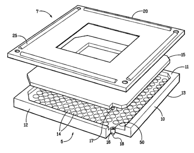
FIG. 1 is a ball grid array socket unit 5 that includes socket assembly 7 in
accordance with the present invention and an electrical component 15 for
insertion therein. The
ball grid array socket assembly 7 includes a socket 10 and a loading device
20. The socket IO
includes housing I2 having a bottom surface 13 and top surface I 1 with a
plurality of apertures
14 therethrough. In one embodiment, the housing 12 is made from a plastic
material; however,
the housing I2 may be made from any suitable material without departing from
the principles of
the present invention.
The socket also includes a plurality of terminals 16 disposed within the
apertures
14. In one embodiment of the present invention, the terminals 16 are made of
copper, however,
5
CA 02406507 2002-10-03
FCI-2577/C2800 PATENT
any suitable material may be used for the terminals I6 without departing from
the scope of the
present invention. Additionally, each terminal 16 may have a contact 18
disposed an the
terminal 16 for electrically connecting the socket 10 to another electrical
device, eg, a printed
circuit board (not shown).
S In accordance with one embodiment of the present invenrion, a compressible
shucture of electrical conductive material SO is disposed within each of the
plurality of terminals
16. As such, when the electrical device 1 S having contacts 17 is placed in
the socket 10, the
contacts I7 of the device 1S depress the compressible structure SO in the
terminals 16 such that
an electrical connection is formed between the terminal I6 and the device I S.
Additionally, in another embodiment of the present invention, the socket
assembly 7 includes a stainless steel loading device 20 for securing an
electrical device 1 S to the
socket 10. In this manner, the loading device 20 may. utilize any conventional
fastening structure
to secure the device 1S to the socket 10. As shown in FIG. 1, the loading
device 20 has apertures
2S therein such that screws, rivets, or the like may be inserted through the
loading device 20 to
1 S fasten the loading device 20 to the socket 10 thereby securing the device
1 S in the socket 10 as
well. Other fastening structures such as hinges or clamps may be used to
connect the loading
device 20 to the socket 10 (and the electrical device 1 S to the socket 10)
without departing from
the scope of the present invention.
In one embodiment of the present invention, the loading device 20 has springs
(not shown) disposed on the surface between the loading device 20 and the
socket 10. In this
manner, when the loading device 20 is secured to the socket 10, the springs
provide a uniform
load against the socket 10. Such a configuration prevents uneven load
distribution that may
6
CA 02406507 2002-10-03
FCI-2577/C2800 PATENT
result in structural bending and/or physical damage to the socket 10, loading
device 20 and/or
device 15.
FIG. 2 is a terminal 16 illustrative of an aspect of the present invention.
The
terminal 16 may be cup-like having an open end 77 and a closed end 79 with
ball contact 18
disposed on the closed end 79 of the terminal 16. The ball contact 18 is used
to electrically
connect the socket 10 to an external circuit (not shown). In this manner, as
shown in FIG. 2, the
structure of electrically conductive material 50 is a ball of metallic wire
and is disposed in the
terminal 16. As such, when the ball contacts 17 of an electrical device (such
as the device 15 of
FIG.1) are inserted into the terminal 16, the device contact 17 compresses the
ball of electrical
material 50 and an electrical connection between the device (not shown) and
terminal contact 18
is established. In this manner, the socket 10 with device 15 secured thereto,
may be inserted into
an external circuit , such as, for example, a printed circuit board and an
electrical connection may
be established between the device 15 and the circuit.
Additionally, not only does the compressible ball of electrically conductive
1 S material 50 establish an electrical connection between the device and the
substrate (not shown),
but the material SO also provides mechanical support. As such, the
compressible material may
compensate for the dimensional tolerance ranges between the device contact 17
and the terminal
16. For example, manufacturing variations may occur in conventional assemblies
leaving device
contacts with spatial tolerances between the contact and the terminal.
Consequently, without the
compressible structure of electrically conductive material, the tolerances
under certain conditions
may result in spatial gaps between the contacts and the terminals that in turn
may cause lateral
movement of the device contacts while inserted into the terminal. Such
movement causes stress
7
CA 02406507 2002-10-03
FCI-2577/C2800 PATENT
to build between the components that may result in loss of electrical
connection or physical
damage to the contact and/or terminal that could in turn lead to improper
electrical
communication between the device and an external circuit. With a compressible
structure 50
disposed in the terminal 16 in accordance with the present invention,
deformation of structure 50
creates an interference fit between contact 17 and terminal 16 and as such,
any lateral movement
is absorbed by the compressible structure 50 thereby preventing physical
damage and loss of an
electrical connection.
Additionally, the compressible structure SO may also absorb any size
variations of
the components caused by deviations in temperature. For example, the device
contact 17 may
expand and contract as electrical power is passed therethrough, as such, the
compressible
structure SO will absorb the deflection while maintaining a solid reliable
electrical connection
therebetween.
The compressible structure 50 of electrical material may be of any shape. For
example, the structure 50 may be ball-like, as seen in FIG. 2. Alternatively,
the structure may be
shaped as a compressible coil or spring or the like without departing from the
present invention.
Further, persons familiar with ball grid array technology in view of the
present disclosure will
understand that forniing structure 50 may have any suitable shape, including a
circular cross
section, substantially flat strips or any other shape.
FIG. 3 illustrates an exemplary method for establishing an electrical
connection
between an electrical device having a plurality of device contacts and a
socket having a plurality
of terminals, the terminals including a compressible structure of electrically
conductive material
disposed therein. Consequently, once an electrical connection is established
between the socket
8
CA 02406507 2002-10-03
FCI-2577/C2800 PATENT
and the device, an electrical connection may be established between an
external circuit (such as a
printed circuit board) and the socket, thereby electrically connecting the
device to the circuit. It
is also contemplated that the socket may first be placed on the external
circuit and the electrical
device inserted into the socket.
In any event, at step 300, the electrical device is placed above a socket such
that
the device contacts generally align with the terminals of the socket and at
step 310, the device
contacts are downwardly inserted into the terminals such that the device
contacts compress the
compressible structure of electrically conductive material disposed in the
terminal. In this
manner, when the compressible electrically conductive material is compressed,
an electrical
connection results between the socket and the electrical device. In another
embodiment of the
present invention, at step 320, a loading device is secured to the socket such
that the electrical
device is also secured to the socket.
As the foregoing illustrates, the present invention is directed to a ball grid
array
socket assembly. It is understood that changes may be made to the embodiments
described above
without departing from the broad inventive concepts thereof. For example,
various loading
devices and fastening structures may be used without departing from the scope
of the present
invention. Accordingly, the present invention is not limited to the particular
embodiments
disclosed, hut is intended to cover all modifications that are within the
spirit and scope of the
invention, as defined by the appended claims.
9