Note: Descriptions are shown in the official language in which they were submitted.
CA 02406707 2002-09-12
WO 01/77641 PCT/USO1/11095
MICROFLUIDIC DEVICES AND SYSTEMS INCORPORATING
COVER LAYERS
CROSS-REFERENCES TO RELATED APPLICATIONS
Pursuant to 35 U.S.C. ~~ 119 and/or 120, and any other applicable
statute or rule, this application claims the benefit of and priority to USSN
09/544,711,
filed on April 6, 2000, the disclosure of which is incorporated by reference.
BACKGROUND OF THE INVENTION
As has been the case in the electronics and computer industries, trends in
analytical chemical and biochemical instrumentation have been toward
miniaturization.
In chemical and biochemical analyses, such miniaturization as achieved in
e.g.,
microfluidic systems, provides numerous advantages, including significantly
smaller
reagent requirements, faster throughput, ready automatability, and in many
cases,
improved data.
By way of example, U.S. Patent Nos. 5,498,392 and 5,587,128 describe
the performance of amplification reactions in microfabricated devices
including
microscale flow systems and/or reaction chambers. Such systems substantially
reduce
the requirements for expensive reagents utilized in amplification reactions.
Further, the
small scale of these devices also provides for enhanced thermal transfer
between
heating sources and the reagents in the device.
Similarly, U.S. Patent No. 5,637,469 describes the use of devices having
extremely small internal dimensions for detecting an analyte in a sample via a
binding
assay. Again, the small scale of such devices provides advantages in terms of
small
reagent volumes.
Commonly owned Published International Application No. WO
98/00231 describes the use of microfluidic devices and systems in the
performance of
high-throughput screening assays. Again, these systems reduce the required
volumes
of potentially very expensive test compounds, e.g., drug candidates, library
compounds,
etc.
CA 02406707 2002-09-12
WO 01/77641 PCT/USO1/11095
Despite the numerous advantages realized by the miniaturization of
analytical systems, such miniaturization can provide difficulties in the use
of such
systems, including user handling, reagent delivery or filtration, and system
interfacing
of such devices.
It would therefore be desirable to provide microfluidic devices that
capture the advantages associated with extremely small volumes and dimensions,
without the problems associated with such small-scale devices. The present
invention
meets these and a variety of other needs.
SUMMARY OF THE INVENTION
It is a general object of the present invention to provide microfluidic
methods and devices that combine the advantages of microfluidics with improved
material handling characteristics and reduced costs for manufacturing. The
invention
accomplishes this in one aspect by providing a microfluidic device having a
body
structure that includes a first microscale channel network disposed therein.
The body
structure includes a plurality of ports disposed in a first surface of the
body structure in
which each port is in fluid communication with one or more channels in the
first
channel network. The device also includes a cover layer having a plurality of
apertures
disposed through and in a first surface of the cover layer. The first surface
of the cover
layer is mated to the first surface of the body structure such that the
apertures align with
and are in fluid communication with the ports. The device additionally
includes a
membrane disposed between at least a portion of the first surface of the cover
layer and
the first surface of the body structure such that the membrane is disposed
between at
least one pair of aligned apertures and ports. In preferred embodiments of the
invention, the membranes (e.g., a semi-permeable membrane portion or the like)
include material immobilized thereon, e.g., for sieving aggregations of
material (e.g.,
aggregations of cells, molecules, etc.) and/or for delivering various reagents
to the
devices.
In another aspect, the invention relates to a microfluidic device having a
body structure that includes a first microscale channel network disposed
therein. The
body structure includes a plurality of ports disposed in a first surface of
the body
structure in which each port is in fluid communication with one or more
channels in the
first channel network. Each of the plurality of ports further includes a rim
disposed
circumferentially around each port in the first surface of the body structure
and an
2
CA 02406707 2002-09-12
WO 01/77641 PCT/USO1/11095
internal surface in which at least a portion of the rim and the internal
surface of at least
one of the plurality of ports includes a conductive coating. The use of
conductive
coatings in the invention, inter alia, minimizes cross-contamination between
microfluidic devices. The device also has a cover layer that includes a
plurality of
apertures disposed through and in a first surface of the cover layer. The
first surface of
the cover layer is mated to the first surface of the body structure such that
the apertures
align with and are in fluid communication with the ports. In certain
embodiments, the
device also includes a membrane (e.g., a semi-permeable membrane portion or
the like)
disposed between at least a portion of the first surface of the cover layer
and the first
surface of the body structure such that the membrane is disposed between at
least one
pair of aligned apertures and ports. In these embodiments, at least a portion
of the
membrane disposed between the at least one pair of aligned apertures and ports
is
conductively connected to the conductive coating.
The invention additionally provides a microfluidic device having a body
structure that includes a first microscale channel network disposed therein.
The body
structure includes a plurality of ports disposed in a first surface of the
body structure in
which each port is in fluid communication with one or more channels in the
first
channel network. The device also includes a cover layer that includes a
plurality of
apertures extending from a first surface to an opposing second surface in
which each of
the plurality of apertures further includes a rim disposed circumferentially
around each
aperture in the second surface of the cover layer and an internal surface. At
least a
portion of the rim and the internal surface of at least one of the plurality
of apertures
include a conductive coating. Optionally, the device also includes a membrane
(e.g., a
semi-permeable membrane portion or the like) disposed between a portion of the
first
surface of the cover layer and the first surface of the body structure such
that the
membrane is disposed between at least one pair of aligned apertures and ports.
As an
additional option, at least a portion of the membrane disposed between the at
least one
pair of aligned apertures and ports is conductively connected to the
conductive coating.
In yet another aspect, the invention relates to a microfluidic device that
includes a body structure having a first microscale channel network disposed
therein.
The body structure has a plurality of ports disposed in a first surface of the
body
structure in which each port is in fluid communication with one or more
channels in the
first channel network. The device also includes a cover layer that includes a
plurality
3
CA 02406707 2002-09-12
WO 01/77641 PCT/USO1/11095
of apertures disposed through and in a first surface of the cover layer. The
first surface
of the cover layer is mated to the first surface of the body structure such
that the
apertures align with and are in fluid communication with the ports. In
addition, the
device includes a plurality of rings in which each of the rings is disposed
between the
cover layer and the body structure and circumferentially around at least one
of the
plurality of apertures and circumferentially around at least one of the
plurality of ports
aligned with one or more of the plurality of apertures. Optionally, at least
one of the
plurality of rings is integral with the body structure, the cover layer, or
both (i.e., the
body structure and the cover layer).
In certain embodiments, the device also includes a membrane (e.g., a
semi-permeable membrane portion or the like) disposed between at least a
portion of
the first surface of the cover layer and the first surface of the body
structure such that
the membrane is disposed between at least one pair of aligned apertures and
ports in
which at least a portion of at least one surface of at least one of the
plurality of rings
includes the membrane. Each well (e.g., each aligned port, ring, and aperture)
of the
devices of the invention typically further includes a rim disposed
circumferentially
around the well in the aperture (e.g., in an annular ridge or the like), in
the ring, or in
the port and an internal surface. Optionally, at least a portion of the rim
and the
internal surface of at least one well includes a conductive coating. In other
embodiments, the device further includes a membrane (e.g., a semi-permeable
membrane portion) disposed between a portion of the first surface of the cover
layer
and the first surface of the body structure such that the membrane is disposed
between
at least one pair of aligned apertures and ports. As an additional option, at
least a
portion of a surface of at least one of the plurality of rings includes the
membrane and
at least a portion of the membrane disposed between the at least one pair of
aligned
apertures and ports is conductively connected to the conductive coating.
The cover layer of the devices of the invention generally includes a
second surface opposite the first surface in which the apertures extend from
the first
surface to the second surface. The cover layer also typically includes a
plurality of
raised annular ridges disposed on the second surface, which annular ridges
surround
each of the apertures. Optionally, a membrane (e.g., a semi-permeable membrane
portion or the like) is disposed over at least one annular ridge surrounding
an aperture
on the second surface.
4
CA 02406707 2002-09-12
WO 01/77641 PCT/USO1/11095
In some embodiments, the cover layer is bonded or clamped to the first
surface of the body structure in the devices of the present invention. The
cover layer
typically further includes a first alignment structure for aligning the body
structure on
the first surface of the cover layer. Optionally, the cover layer includes a
second
alignment structure complementary to an alignment structure on a
controller/detector
apparatus to align the microfluidic device in the controller/detector
apparatus.
The present invention also includes methods of controlling a material
composition delivered into a microfluidic device which include flowing a
solution that
includes the material (e.g., particles, reagents, or the like) through a semi-
permeable
membrane portion disposed in one or more wells of the devices. Additionally,
the
methods optionally include immobilizing the material on the semi-permeable
membrane prior to delivering the material into the device.
In a related aspect, the present invention provides a microfluidic system
that includes a microfluidic device in accordance with the present invention,
where the
device is further mounted on a controller/detector apparatus that is
configured to
receive the microfluidic device. The controller/detector apparatus comprises
an optical
detection system and a material transport system, where the detection system
and
transport system are operably interfaced with the microfluidic device when the
device
is mounted on the controller/detector.
BRIEF DESCRIPTION OF THE FIGURES
Figure 1 schematically illustrates a microfluidic device body structure
that incorporates a planar layered structure.
Figures 2A-E illustrate from a number of perspectives an embodiment of
a cover layer for incorporation in a microfluidic device in accordance with
the present
invention.
Figure 2F illustrates the interaction of a filling device with the
microfluidic devices of the invention.
Figure 3A illustrates a fully assembled microfluidic device that includes
the layered body structure of Figure 1 and the cover layer of Figure 2 mated
together.
Figure 3B illustrates an alternate mechanism for joining the body
structure to the cover layer in the fully assembled device.
CA 02406707 2002-09-12
WO 01/77641 PCT/USO1/11095
DETAILED DESCRIPTION OF THE INVENTION
General
The present invention generally provides microfluidic devices and
methods that take advantage of the extremely small-scale nature of
microfluidic devices
and systems, while at the same time, not suffering from some of the potential
problems
associated with such systems. In particular, the microfluidic devices and
systems of the
invention include an additional cover layer as a portion of the microfluidic
device, e.g.,
overlaying and attached to the basic body structure of the device. The cover
layer
employed in the devices of the invention typically comprises a number of
apertures
disposed through it, which apertures mate with and/or form part of the
reservoirs and/or
access ports of the microfluidic device. These cover layers provide a number
of
advantages in the operation and fabrication of microfluidic devices.
As used herein, the terms "microscale," "microfabricated" or
"microfluidic" generally refer to one or more fluid passages, chambers or
conduits which
have at least one internal cross-sectional dimension, e.g., depth, width,
length, diameter,
etc., that is less than 500 Vim, and typically between about 0.1 ~m and about
500 pm. In
the devices of the present invention, the microscale channels or chambers
preferably have
at least one cross-sectional dimension between about 0.1 ~m and 200 pm, more
preferably between about 0.1 ~m and 100 p,m, and often between about 0.1 pm
and 20
pm. Accordingly, the microfluidic devices or systems prepared in accordance
with the
present invention typically include at least one microscale channel, usually
at least two
intersecting microscale channels, and often, three or more intersecting
channels disposed
within a single body structure. Channel intersections may exist in a number of
formats,
including cross intersections, "T" intersections, or any number of other
structures
whereby at least two channels are in fluid communication.
The body structure of the microfluidic devices described herein can take a
variety of shapes and/or conformations, provided the body structure includes
at least one
microfluidic channel element disposed within it. For example, in some cases
the body
structure has a tubular conformation, e.g., as in capillary structures, such
as fused silica or
polymeric capillaries that include internal diameters in the microscale range,
set forth
above. Alternatively, body structures may incorporate non-uniform shapes
and/or
conformations, depending upon the application for which the device is to be
used. In
6
CA 02406707 2002-09-12
WO 01/77641 PCT/USO1/11095
preferred aspects, the body structure of the microfluidic devices incorporates
a planar or
"chip" structure.
Although in some cases, a single piece body structure, e.g., a capillary,
may be used, the devices described herein typically comprise an aggregation of
two or
more separate layers which when appropriately mated or joined together, form
the body
structure of the microfluidic device of the invention, e.g., containing the
channels and/or
chambers described herein. Typically, the microfluidic devices described
herein will
comprise a top portion, a bottom portion, and an interior portion, wherein the
interior
portion substantially defines the channels and chambers of the device.
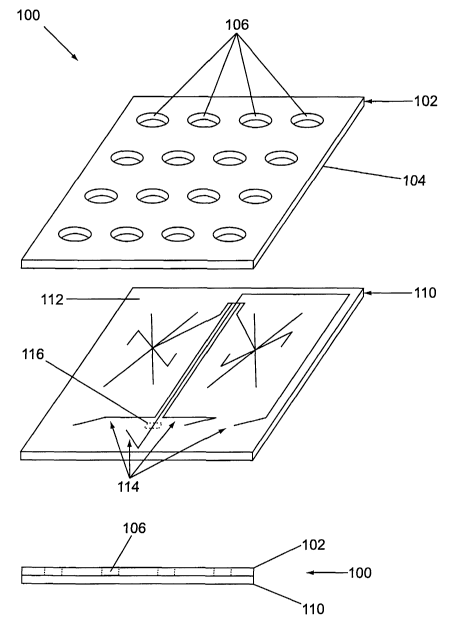
Figure 1 illustrates one example of the body structure of a microfluidic
device that incorporates a planar, layered structure. As shown, the body
structure 100
includes at least two layers, an upper layer 102 and a lower layer 110. The
upper surface
112 of the lower layer 110 is fabricated to include grooves and/or wells 114.
The lower
surface 104 of the upper layer 102 is then mated to the upper surface 112 of
the lower
layer 110 such that the grooves and/or channels define channels or conduits,
and
chambers within the interior of the aggregate body structure.
A variety of substrate materials may be employed as the bottom portion.
Typically, because the devices are microfabricated, substrate materials will
be selected
based upon their compatibility with known microfabrication techniques, e.g.,
photolithography, wet chemical etching, laser ablation, reactive ion etching
(RIE), air
abrasion techniques, injection molding, LIGA methods, metal electroforming,
embossing,
and other techniques. Suitable substrate materials are also generally selected
for their
compatibility with the full range of conditions to which the microfluidic
devices may be
exposed, including extremes of pH, temperature, salt concentration, and
application of
electric fields. Accordingly, in some preferred aspects, the substrate
material may
include materials normally associated with the semiconductor industry in which
such
microfabrication techniques are regularly employed, including, e.g., silica
based
substrates, such as glass, quartz, silicon or polysilicon, as well as other
substrate
materials, such as gallium arsenide and the like. In the case of
semiconductive materials,
it will often be desirable to provide an insulating coating or layer, e.g.,
silicon oxide, over
the substrate material, and particularly in those applications where electric
fields are to be
applied to the device or its contents. In preferred aspects, the substrates
used to fabricate
the body structure are silica-based, and more preferably glass or quartz, due
to their
7
CA 02406707 2002-09-12
WO 01/77641 PCT/USO1/11095
inertness to the conditions described above, as well as the ease with which
they are
microfabricated.
In alternate preferred aspects, the substrate materials comprise polymeric
materials, e.g., plastics, such as polymethylmethacrylate (PMMA),
polycarbonate,
polytetrafluoroethylene (TEFLONT"~), polyvinylchloride (PVC),
polydimethylsiloxane
(PDMS), polysulfone, polystyrene, polymethylpentene, polypropylene,
polyethylene,
polyvinylidine fluoride, ABS (acrylonitrile-butadiene-styrene copolymer), and
the like.
Such polymeric substrates are readily manufactured using available
microfabrication
techniques, as described above, or from microfabricated masters, using well
known
molding techniques, such as injection molding, embossing or stamping, or by
polymerizing the polymeric precursor material within the mold (See U.S. Patent
No.
5,512,131). Again, such polymeric substrate materials are preferred for their
ease of
manufacture, low cost and disposability, as well as their general inertness to
most
extreme reaction conditions. Again, these polymeric materials may include
treated
surfaces, e.g., derivatized or coated surfaces, to enhance their utility in
the microfluidic
system, e.g., provide enhanced fluid direction, e.g., as described in U.S.
Patent No.
5,885,470, and which is incorporated herein by reference in its entirety for
all purposes.
In the embodiment shown, the upper layer 102 of the body structure 100,
includes a plurality of ports 106 disposed through it. These ports are
positioned to
communicate with specific points of the channels or grooves 114, e.g., the
termini, in the
aggregate body structure when the upper and lower layers are mated. The ports
106
function to provide fluid access to the channels of the device, and in certain
aspects,
electrical access to the channels within the body structure. As discussed
further below,
rings are optionally molded around (i.e., surround) one or more of the
plurality of ports
on the upper surface of the upper layer of the body structure. Additionally,
at least a
portion of the ports also optionally includes a conductive coating so that
electrical
communication is optionally achieved in the device without placing electrodes
directly
into, e.g., the ports. The use of conductive coatings is also described
further below.
In many embodiments, the microfluidic devices include an optical
detection window 116 disposed across one or more channels and/or chambers of
the
device. Optical detection windows are typically transparent such that they are
capable of
transmitting an optical signal from the channel/chamber over which they are
disposed.
Optical detection windows may merely be a region of a transparent layer of the
body
structure, e.g., where the layer is glass or quartz, or a transparent polymer
material, e.g.,
8
CA 02406707 2002-09-12
WO 01/77641 PCT/USO1/11095
PMMA, polycarbonate, etc. Alternatively, where opaque substrates are used in
manufacturing the devices, transparent detection windows fabricated from the
above
materials may be separately manufactured into the device.
Microfluidic devices may be used in a variety of applications, including,
e.g., the performance of high throughput screening assays in drug discovery,
immunoassays, diagnostics, genetic analysis, and the like. As such, the
devices
described herein, will often include multiple sample introduction ports or
reservoirs, for
the parallel or serial introduction and analysis of multiple samples.
Alternatively, these
devices may be coupled to a sample introduction port, e.g., a pipettor, which
serially
introduces multiple samples into the device for analysis. Examples of such
sample
introduction systems are described in, e.g., U.S. Patent Nos. 6,046,056 and
5,880,071,
each of which is hereby incorporated by reference in its entirety for all
purposes. As
discussed below, the invention also includes methods and devices that utilize
membranes for sieving aggregations of material (e.g., clumps of cells,
reagents, or other
particles) and otherwise delivering reagents or other materials into the ports
of the
devices.
In preferred aspects; the microfluidic devices of the present invention
utilize electrokinetic material transport systems to direct and transport
materials
through the channels of the device. As used herein, "electrokinetic material
transport"
generally refers to systems and methods for transporting and directing
materials within
an interconnected channel and/or chamber containing structure, through the
application
of electrical fields to the materials, thereby causing material movement
through and
among the channels and/or chambers, i.e., canons will move toward the negative
electrode, while anions will move toward the positive electrode.
Such electrokinetic material transport and direction systems include
those systems that rely upon the electrophoretic mobility of charged species
within the
electric field applied to the structure. Such systems are more particularly
referred to as
electrophoretic material transport systems. Other electrokinetic material
direction and
transport systems rely upon the electroosmotic flow of fluid and material
within a
channel or chamber structure, either alone, or in conjunction with the
electrophoretic
forces previously described, which electroosmotic flow results from the
application of
an electric field across such structures. In brief, when a fluid is placed
into a channel
which has a surface bearing charged functional groups, e.g., hydroxyl groups
in etched
9
CA 02406707 2002-09-12
WO 01/77641 PCT/USO1/11095
glass channels or glass microcapillaries, those groups can ionize. In the case
of
hydroxyl functional groups, this ionization, e.g., at neutral pH, results in
the release of
protons from the surface and into the fluid, producing a concentration of
protons near
the fluid/surface interface, and creating a positively charged sheath
surrounding the
bulk fluid in the channel. Application of a voltage gradient across the length
of the
channel, causes the proton sheath to move in the direction of the voltage
drop, i.e.,
toward the negative electrode. Flow in the opposite direction is achieved by
either
reversing the voltage gradient, or by providing a channel bearing positively
charged
ionizable groups, e.g., amino groups, etc.
"Controlled electrokinetic material transport and direction," as used
herein, refers to electrokinetic systems as described above, which employ
active control
of the voltages applied at multiple, i.e., more than two, electrodes.
Rephrased, such
controlled electrokinetic systems concomitantly regulate voltage gradients
applied
across at least two intersecting channels. Controlled electrokinetic material
transport is
described in Published PCT Application No. WO 96/04547, to Ramsey, which is
incorporated herein by reference in its entirety for all purposes. In
particular, the
preferred microfluidic devices and systems described herein, include a body
structure
which includes at least two intersecting channels or fluid conduits, e.g.,
interconnected,
enclosed chambers, which channels include at least three unintersected
termini. The
intersection of two channels refers to a point at which two or more channels
are in fluid
communication with each other, and encompasses "T" intersections, cross
intersections,
"wagon wheel" intersections of multiple channels, or any other channel
geometry
where two or more channels are in such fluid communication. An unintersected
terminus of a channel is a point at which a channel terminates not as a result
of that
channel's intersection with another channel, e.g., a "T" intersection. In
preferred
aspects, the devices will include at least three intersecting channels having
at least four
unintersected termini. In a basic cross channel structure, where a single
horizontal
channel is intersected and crossed by a single vertical channel, controlled
electrokinetic
material transport operates to controllably direct material flow through the
intersection,
by providing constraining flows from the other channels at the intersection.
For
example, assuming one was desirous of transporting a first material through
the
horizontal channel, e.g., from left to right, across the intersection with the
vertical
channel. Simple electrokinetic material flow of this material across the
intersection
CA 02406707 2002-09-12
WO 01/77641 PCT/USO1/11095
could be accomplished by applying a voltage gradient across the length of the
horizontal channel, i.e., applying a first voltage to the left terminus of
this channel, and
a second, lower voltage to the right terminus of this channel, or by allowing
the right
terminus to float (applying no voltage). However, this type of material flow
through
the intersection would result in a substantial amount of diffusion at the
intersection,
resulting from both the natural diffusive properties of the material being
transported in
the medium used, as well as convective effects at the intersection.
In controlled electrokinetic material transport, the material being
transported across the intersection is constrained by low level flow from the
side
channels, e.g., the top and bottom channels. This is accomplished by applying
a slight
voltage gradient along the path of material flow, e.g., from the top or bottom
termini of
the vertical channel, toward the right terminus. The result is a "pinching" of
the
material flow at the intersection, which prevents the diffusion of the
rmaterial into the
vertical channel. The pinched volume of material at the intersection may then
be
injected into the vertical channel by applying a voltage gradient across the
length of the
vertical channel, i.e., from the top terminus to the bottom terminus. In order
to avoid
any bleeding over of material from the horizontal channel during this
injection, a low
level of flow is directed back into the side channels, resulting in a "pull
back" of the
material from the intersection.
In addition to pinched injection schemes, controlled electrokinetic
material transport is readily utilized to create virtual valves that include
no mechanical
or moving parts. Specifically, with reference to the cross intersection
described above,
flow of material from one channel segment to another, e.g., the left arm to
the right arm
of the horizontal channel, can be efficiently regulated, stopped and
reinitiated, by a
controlled flow from the vertical channel, e.g., from the bottom arm to the
top arm of
the vertical channel. Specifically, in the 'off mode, the material is
transported from the
left arm, through the intersection and into the top arm by applying a voltage
gradient
across the left and top termini. A constraining flow is directed from the
bottom arm to
the top arm by applying a similar voltage gradient along this path (from the
bottom
terminus to the top terminus). Metered amounts of material are then dispensed
from
the left arm into the right arm of the horizontal channel by switching the
applied
voltage gradient from leftaop, to left:right. The amount of time and the
voltage
gradient applied dictates the amount of material that will be dispensed in
this manner.
11
CA 02406707 2002-09-12
WO 01/77641 PCT/USO1/11095
In particularly preferred aspects, electrokinetic material transport is
controlled through the application of appropriate currents through the
channels of the
system, in order to propagate material movement therethrough. The use of
current
control in electrokinetic material transport systems is described in detail in
commonly
owned U.S. Patent No. 5,800,690 and Published PCT Application No. 98/00707,
both
of which are incorporated herein by reference. In brief, in electrokinetic
material
transport systems, the relative potentials at the intersections of the
channels dictates the
direction and velocity of material movement at those intersections. Control of
these
potentials has typically relies upon the calculation of applied voltages based
upon the
desired potential at the intersections and the resistance of the channel
between the
intersection and the electrodes at which voltages are applied. By monitoring
and
controlling the current, the potential at the intersection is maintained at
the desired
level, and the applied voltages are self-regulating.
Although described for the purposes of illustration with respect to a four
way, cross intersections, these controlled electrokinetic material transport
systems can
be readily adapted for more complex interconnected channel networks, e.g.,
arrays of
interconnected parallel channels. As discussed further below, electrokinetic
material
transport systems also optionally include the use of conductive coatings to
achieve
electrical communication.
A. Physical and Electrical Isolation of Reservoirs/Ports
As noted previously, in the design and fabrication of microfluidic
systems, and underlying goal is to miniaturize the entire system. This is
typically done
either to reduce volume, increase the speed of the operation, or multiplex the
particular
operation, e.g., incorporate multiple operations within the same unit space
occupied by
the device. In accomplishing these goals, however, the channel networks that
effectively define the functional space of a given microfluidic system become
much
smaller. As a result of smaller channel networks, or more complex networks
being
incorporated into the same unit space, the access points for these channel
networks,
e.g., reservoirs, electrical access ports and the like, are drawn closer and
closer
together.
As these access ports are drawn closer together, it becomes more
difficult to practically isolate one port from another. For example, where the
access
ports are used to introduce fluids into the channel networks of the system,
the closer the
12
CA 02406707 2002-09-12
WO 01/77641 PCT/USO1/11095
ports are together or the smaller they become, the more difficult it becomes
to introduce
fluid volumes separately into different ports. This is true for manual
introduction of
fluids, e.g., using a pipettor, as well as automatic methods, e.g., using
robotic fluid
handling systems.
In a similar problem, as access ports are placed closer together, it also
becomes more difficult to isolate those ports electrically. This is of
particular
importance in microfluidic systems that utilize electrical systems operably
coupled to
the channel networks, such as in electrical sensing systems, e.g.,
amperometric,
potentiometric, etc., and/or electrokinetic material transport that are used
for transport
of materials through the channel networks, as described above. In particular,
where the
ports of the system are used for electrical access, the possibility of
bridging currents, or
"shorts," between two or more adjacent or at least proximal electrodes
increases, e.g.,
across the surface of the device as a result of fluids, dirt or oils deposited
on the surface
of the device.
The present invention generally addresses these problems by providing
microfluidic devices that include a cover layer that provides an effective
barrier
between neighboring reservoirs, to prevent fluid and/or electrical links from
forming
between neighboring electrodes. The barrier optionally includes a ridge around
each of
the reservoirs, e.g., an annular ridge surrounding a circular reservoir. The
ridge has the
effect of preventing fluid 'spill-over' from one well entering into another
adjacent well.
Similarly, the ridge effectively creates a longer path length across which any
electrical
bridging current, e.g., short circuit, must travel. Typically, these ridges
extend at least
0.1 mm from the surface of the cover layer, preferably, at least 1 mm and in
some
1 cases, at least 2 mm or more, from the upper surface of the cover layer. In
many cases,
the barner, e.g., as provided by the ridge structure, will increase the
effective path
length between neighboring wells by at least 1.5X, preferably at least 2X, and
often at
least 3-5X over that provided by the reservoirs in the body structure, alone.
The use of separate or integrated holding structures for microfluidic
devices is described in commonly owned U.S. Patent No. 5,876,675 and
incorporated
herein by reference in its entirety for all purposes.
In addition to providing an effective barner between neighboring
reservoirs, in some cases, the upper surface comprises a hydrophobic material
to
prevent deposition/aggregation of fluids on that surface which might
physically or
13
CA 02406707 2002-09-12
WO 01/77641 PCT/USO1/11095
electrically contaminate neighboring reservoirs. In such cases, a hydrophobic
material,
e.g., a polymer, is coated on the surface of the cover layer. Preferably,
however, and as
described in greater detail below, the cover layer itself is fabricated from a
hydrophobic
polymer material.
B. Increased Volume Capacity of Reservoirs
The cover layer component of the microfluidic devices of the present
invention also provides the capability to increase the volume capacity of the
reservoirs
of those devices. In particular, the apertures disposed in the cover layer can
increase
the total depth of the fluid reservoirs of the device by extending those
reservoirs. While
fluid volume is not a critical limitation in many microfluidic applications,
there are
some instances where substantial variations in fluid volume from, e.g.,
evaporation, can
have an effect on a particular operation. This is typically due to
concentration of one or
more solutes within the fluids, e.g., salts, enzymes, etc. By increasing the
fluid volume
capacity of the reservoirs, one can substantially mitigate any effects
resulting from a
partial evaporation of fluids by reducing the percentage of evaporation.
Typically, the apertures disposed in the cover layer add to the depth of
the reservoirs in the body structure. In doing so, the apertures are typically
at least 1
mm deep, preferably at least 2 mm deep, and often at least 5 mm deep. This
typically
results in reservoirs in the overall device, e.g., from the combination of the
ports in the
body structure and the apertures in the cover layer, having volumes of at
least 5 ~1,
preferably at least 10 ~1, more preferably at least 20 ~,1, often at least 50
~1, and in some
cases, at least 100 ~l. In any event, the volume of the reservoirs of the
overall device
will typically fall in the range between about 1 and about 200 p1, preferably
between
about 2 and 100 ~l, more preferably between about 5 and about 100 ~1, and
still more
preferably, between about 5 and 50 p1.
II. Fabrication of Cover Layers
The cover layer aspect of the microfluidic devices described herein may
generally be fabricated from any of a number of different materials using a
number of
different methods. For example, the materials and methods described above in
the
manufacture of the microfluidic elements of the device may also be employed in
the
manufacture of the cover layer. While these methods are effective, in
preferred aspects,
more conventional manufacturing techniques are used to produce the cover
layer. In
14
CA 02406707 2002-09-12
WO 01/77641 PCT/USO1/11095
particular, because the cover layer does not need to be manufactured to the
tolerances
of the microfluidic elements of the devices of the invention, they can
generally be
manufactured using less precise and less expensive or time consuming methods
and
from less costly materials.
For example, in a layered microfluidic device fabricated from two glass
layers, fabrication of the ports or reservoirs in one layer, e.g., by drilling
or air abrasion
techniques, can take a substantial amount of time. Further, the amount of time
required
for such fabrication increases in a non-linear, e.g., exponential, fashion
with increasing
substrate thickness. Conversely, reduction of substrate thickness reduces the
amount of
time required to fabricate the reservoirs, in an exponential fashion. Because
a portion
of the volume of the reservoirs in the final microfluidic device is optionally
supplied by
the cover layer element, the substrate layers used to fabricate the body
structure of the
microfluidic device can be substantially thinner. Specifically, less of the
total desired
volume of the reservoir is a function of substrate thickness. As a result,
fabrication
time and cost associated with the manufacturing of reservoirs in the body
structure are
substantially reduced.
Typically, the cover layer comprises an injection molded polymeric or
plastic part, fabricated from any of a number of different manufacturable
plastics. For
example, the cover layer is typically fabricated from any of the polymeric
materials
described above for fabricating the body structure of the microfluidic device,
e.g.,
polymethylmethacrylate (PMMA), polycarbonate, polytetrafluoroethylene
(TEFLONT"'), polyvinylchloride (PVC), polydimethylsiloxane (PDMS),
polysulfone,
polystyrene, polymethylpentene, polypropylene, polyethylene, polyvinylidine
fluoride,
ABS, and the like. In alternate aspects, the cover layer is optionally
fabricated from
non-polymeric materials, e.g., silica-based substrates, such as glass, quartz,
silicon, as
well as ceramics or metals.
Attachment of the cover layer to the body structure of the device is also
typically accomplished by well known methods, including adhesive bonding,
ultrasonic
welding, solvent welding, thermal bonding, and the like. In preferred aspects,
the cover
layer is attached to the body structure of the device using an adhesive
material, and
more preferably, U.V. curable adhesives are used to join the cover layer with
the body
structure. Such adhesives are generally commercially available, e.g., from 3M
Corporation. In particularly preferred aspects, the selected adhesive is
electrically
CA 02406707 2002-09-12
WO 01/77641 PCT/USO1/11095
insulating, e.g., nonconductive, non-soluble and/or non-leaching in
application buffers,
low fluorescing, and the like.
In a preferred embodiment of the present invention, the microfluidic
device includes a plurality of rings disposed around the reservoirs or ports
in the
microfluidic device underlying the cover layer. The rings are optionally
molded around
the apertures on the first surface of the cover layer and integral with the
cover layer.
Alternatively, the rings are molded around the ports disposed in the first
surface of the
body structure and integral with the body structure. As an additional
alternative, the
rings are separate from the cover layer and the body structure. Upon
attachment of the
cover layer to the body structure, a ring becomes disposed between each
aperture
aligned with each port. As discussed further below, the rings also optionally
include
conductive coatings and/or membranes.
The rings act to prevent adhesive, e.g., U.V. curable adhesive
(mentioned above), from getting into the ports and in turn from contacting any
assay
components that are in the ports. As such, rings are optionally shaped as
circular rings
or as any other functionally equivalent forms, e.g., rectangular or polygonal
rings. In
the context of rings, the terms "thick" and/or "thickness" refer to the
distance from an
inner edge to an outer edge of a ring. A ring has a single thickness, as in-
the case of
circular rings, or multiple thicknesses when other ring shapes are selected.
However,
each ring typically has a thickness in the range of from about 1 ~M to about
1,000 ~M.
For example, the rings are optionally in the range of from about 50 ~M to
about 750
~,M thick, e.g., about S00 ~M thick. Larger rings typically result in the
creation of
voids around the ports/apertures. Narrower rings, e.g., in the range of from
about 100
~M to about 500 ~M are generally preferred.
The rings are optionally fabricated from many different materials. For
example, if they are integral with the cover layer or the body structure, they
are made
from the same material, and in the same step, as either of those two
respective
components. As discussed above, these optionally include a wide variety of
polymeric
and non-polymeric materials. If the rings are separate from the cover layer
and the
body structure, they are also optionally fabricated from any of the polymeric
or non-
polymeric materials discussed above as well as others, including
polymethylmethacrylate (PMMA), polycarbonate, polytetrafluoroethylene
(TEFLONT""), polyvinylchloride (PVC), polydimethylsiloxane (PDMS),
polysulfone,
16
CA 02406707 2002-09-12
WO 01/77641 PCT/USO1/11095
polystyrene, polymethylpentene, polypropylene, polyethylene, polyvinylidine
fluoride,
ABS (acrylonitrile-butadiene-styrene copolymer), glass, quartz, silicon,
gallium
arsenide, silicon oxide, ceramics, metals, latex, silicone, or the like.
In alternate aspects, the body structure is attached to the cover layer via
a clamping mechanism. In such aspects, an optional flexible gasket, e.g.,
latex,
silicone, etc., is placed between the upper surface of the body structure and
the lower
surface of the cover layer. The flexible gaskets also optionally include the
rings,
discussed above, as integral components therein. The body structure is then
compressively clamped against the cover layer forming a sealed, joined
structure.
Suitable clamping mechanisms may be separate from the body structure/cover
layer
assembly, i.e., screw clamps, clip-style clamps, e.g., that clamp the edges of
the body
structure and cover layer, and the like. Alternatively, integrated clamping
mechanisms
are provided as a portion of the cover layer, into which the body structure is
snapped.
Such clamping systems are described in greater detail below, with reference to
Figure
3B.
III. Microfluidic Devices and Methods Incorporating Membranes and/or
Conductive Coatings
In general, the process of developing operable and commercially
valuable microfluidic devices typically includes overcoming various technical
hurdles.
For example, one technical problem in the development of practical cell-based
microfluidic assays has been eliminating cell clumps or aggregations that clog
microscale channels, rendering the devices inoperable. Another challenge has
been to
create functional reagent delivery systems for integrating reagents into
microfluidic
devices such that they will dissolve, e.g., in a sample. An additional problem
has been
cross-contamination among microfluidic devices when, e.g., electrodes are used
in
multiple devices. The present invention provides various solutions to all of
these
technical problems; solutions which are optionally used alone or in
combination in the
same device.
For example, the present invention provides methods of controlling a
material composition delivered into a microfluidic device. The methods include
providing a channel network disposed in the microfluidic device and at least
one well in
fluid communication with the channel network. The well includes a semi-
permeable
membrane portion disposed therein or thereon. As a first option, the methods
also
17
CA 02406707 2002-09-12
WO 01/77641 PCT/USO1/11095
include flowing a first solution that includes a material (e.g., particles,
reagents, or the
like) into the well through the semi-permeable membrane portion. A second
option
includes immobilizing the material on the semi-permeable membrane portion and
flowing a second solution into the well of the microfluidic device.
Thereafter, the
second option includes mixing the second solution and the material immobilized
on the
semi-permeable membrane portion such that at least some of the material
dissolves in
the second solution and enters the microfluidic device through the semi-
permeable
membrane portion. The mixing step optionally includes a physical technique,
such as
shaking, vortexing, centrifuging, etc. the microfluidic device to dissolve at
least some
of the material adhered to the semi-permeable membrane portion in the second
solution. In either case, the channel network is at least partially filled
with a fluid prior
to flowing the first or second solutions into the well, or the channel network
is void of
fluid prior to flowing the first or second solutions into the well.
Irrespective of the option selected, aggregations of the material are
sieved and prevented from entering the channel network of the microfluidic
device. As
used herein, the phrase "aggregations of material" refers to clumps or
clusters of the
material, such as a clump of cells, reagent molecules, or the like, which, if
permitted to
enter the device, would likely obstruct the channel network. The semi-
permeable
membranes utilized selectively exclude aggregations of material based upon
size.
Typically, the semi-permeable membrane portion includes a pore size of at
least about
0.1 nm. In preferred embodiments, the semi-permeable membrane portion includes
a
pore size of between about 10 ~m and about 100 Vim, which will exclude clumps
of
cells. The membranes optionally cover at least a portion of a well and are
disposed
between the body structure and the cover layer so as to keep each well sealed
from
other wells. Alternatively, membranes are placed on or over wells.
Suitable semi-permeable membrane portions optionally include, e.g. a
woven mesh membrane, a microfiltration membrane, a nanofiltration membrane, a
dialysis membrane, an electrodialysis membrane, a prevaporation membrane, a
reverse
osmosis membrane, an ultrafiltration membrane, a composite membrane, a charged
membrane, a conductively-coated membrane, a hydrophilic membrane, a
hydrophobic
membrane, a polymer-based membrane, a non-polymer-based membrane, a porous
plastic matrix membrane (e.g., POREX~ Porous Plastic, etc.), a porous metal
matrix
membrane, a polyethylene membrane, a poly(vinylidene difluoride) membrane, a
18
CA 02406707 2002-09-12
WO 01/77641 PCT/USO1/11095
polyamide membrane, a nylon membrane, a ceramic membrane, a polyester
membrane,
a metal membrane, a polytetrafluoroethylene (TEFLONT"") membrane, a
polyaramide
membrane, a polycarbonate membrane, a powdered activated carbon membrane, a
polypropylene membrane, a glass fiber membrane, a glass membrane, a
nitrocellulose
membrane, a cellulose membrane, a cellulose nitrate membrane, a cellulose
acetate
membrane, a polysulfone membrane, a polyethersulfone membrane, a polyolefin
membrane, or the like. A number of publications relating to membranes are also
available, including Cheryan, Ultrafiltration and Microfiltration Handbook
(2°d Ed.)
Technomic Publishing Company, Lancaster, PA (1998), Minder, Basic Principles
of
Membrane Technolo~y (2°d Ed.) Dordrecht: Kluwer (1996), and Ho and
Sirkar (Eds.),
Membrane Handbook Van Nostrand Reinhold, New York (1992).
The methods of the present invention include various materials. In
preferred embodiments, the material includes a particle, such as a cell or a
set of cells.
For example, the material flowed into the well typically includes a plurality
of cells or
sets of cells and the volume of the first solution flowed into the well is
optionally
between about 0.5 and about 20 ~,1, optionally in the range of from about 5 to
about 15
p1, or, e.g., about 10 ~1. Cell sample volumes loaded into wells in this range
are vast
improvements over the several hundreds of microliters typically used, e.g., in
conventional cell filtration techniques. The material also optionally includes
a reagent,
such as an atom, a set of atoms, a molecule, a set of molecules, a bead, a set
of beads, a
functionalized bead, a set of functionalized beads, an antigen, a set of
antigens, a
protein, a set of proteins, a peptide, a set of peptides, an enzyme, a set of
enzymes, a
nucleic acid, a set of nucleic acids, a lipid, a set of lipids, a
carbohydrate, a set of
carbohydrates, an inorganic molecule, a set of inorganic molecules, an organic
molecule, a set of organic molecules, a drug, a set of drugs, a receptor, a
set of
receptors, a ligand, a set of ligands, an antibody, a set of antibodies, a
neurotransmitter,
a set of neurotransmitters, a cytokine, a set of cytokines, a chemokine, a set
of
chemokines, a hormone, a set of hormones, or the like.
As mentioned, the methods of controlling material compositions
optionally include immobilizing the material (e.g., a labeled antibody, a
reagent, or
other particle) on the semi-permeable membrane portion before delivering the
material
into the microfluidic device. Materials are alternately immobilized using
various
techniques or combinations of techniques. Additionally, the immobilizing step
is
19
CA 02406707 2002-09-12
WO 01/77641 PCT/USO1/11095
optionally performed prior to placing the semi-permeable membrane portion on
the at
least one well. In a preferred embodiment, the immobilizing step includes
dehydrating
the first solution that includes the material on the semi-permeable membrane
portion
such that at least some of the material adheres to the semi-permeable membrane
portion. This immobilization approach optionally includes, e.g., air drying,
heat drying,
lyophilizing, using a drying reagent, or the like to dehydrate the first
solution. As
mentioned, this technique optionally includes, e.g., spotting and dehydrating
the first
solution containing the material on the semi-permeable membrane before placing
the
membrane over the well(s).
In another embodiment, the semi-permeable membrane portion includes
a hydrophobic coating, or is composed of a hydrophobic substance, and the
material is
a hydrophobic material so that the material immobilizes on the semi-permeable
membrane portion by hydrophobic attraction. Similarly, the semi-permeable
membrane portion optionally includes a hydrophilic coating, or is composed of
a
hydrophilic substance, and the material is a hydrophilic material so that the
material
immobilizes on the semi-permeable membrane portion by hydrophilic attraction.
Many
hydrophobic and hydrophilic coatings or substances are known and are
optionally used
in the methods and devices of the present invention. For example, suitable
hydrophobic coatings or substances optionally include, e.g., hydrophobic
polymers,
fluorocarbon polymers, chlorinated polysiloxanes, polytetrafluoroethylenes
(TEFLONT""), polyglycines, polyalanines, polyvalines, polyleucines,
polyisoleucines,
chlorine terminated polydimethylsiloxane telomers, bis(perfluorododecyl)
terminated
poly(dimethylsiloxane-co-dimer acids), derivatives thereof, or the like.
TEFLONT"~ is
generally preferred and is readily available from various commercial sources.
Appropriate hydrophilic coatings and substances optionally include, e.g.,
hydrophilic
polymers, polyimides, polyethylene oxides, polyvinylpyrrolidone,
polyacrylates,
hydrophilic polysaccharides, hyaluronic acids, chondroitin sulfates,
derivatives thereof,
or the like.
Other immobilization techniques include, e.g., providing the semi-
permeable membrane portion to include a net charge. In turn, the material
includes a
net charge opposite from the semi-permeable membrane portion so that the
material
immobilizes on the semi-permeable membrane portion by electrostatic
attraction.
CA 02406707 2002-09-12
WO 01/77641 PCT/USO1/11095
The present invention also relates to a microfluidic device that includes
a membrane (e.g., a semi-permeable membrane portion) disposed between at least
a
portion of the first surface of the cover layer and the first surface of the
body structure
such that the membrane is disposed between at least one pair of aligned
apertures and
ports. Aspects of this device are optionally utilized, inter alia, for
controlling material
(e.g., reagents, cells, or other particles) compositions delivered into the
device. The
type of semi-permeable membrane portion used, including the pore size,
optionally
include any of those described above.
As mentioned, in certain cases cross-contamination among microfluidic
devices results, e.g., when electrodes are used in multiple microfluidic
devices. This
form of contamination typically occurs when electrodes are placed directly
into liquids
situated in the wells of the devices. To address this problem, the present
invention
optionally includes the use of conductive coatings that permit the use of dry
contact
electrodes to minimize this type of contamination. Conductive coatings are
optionally
deposited by, e.g., plating, electroforming, vapor deposition, or the like. A
conductive
coating also optionally includes, e.g., a pre-formed piece of metal or other
conductive
material pressed into one or more wells of a device such that the coating
covers at least
a portion of the internal surface of, and extends over the top rim of, one or
more wells.
The conductive coating optionally includes, e.g., a thin ring (or other
functionally
equivalent form) of conductive material pressed into one or more wells of a
device so
that conductive communication is optionally established between the
microchannels of
the device and a conductive source. Suitable conductive coatings are discussed
further
below.
In one embodiment, each of the plurality of ports includes a rim
disposed circumferentially around each port in the first surface of the body
structure
and an internal surface in which at least a portion of the rim and the
internal surface of
at least one of the plurality of ports includes a conductive coating. In this
embodiment,
conductive contact between the conductive coating and an electrode is
optionally
established, e.g., by modifying the cover layer to include a conductive inlet
that is not
in fluid communication with the well, yet which is in conductive communication
with
the conductive coating disposed on the rim and/or internal surface of a port.
The rim
typically includes at least one width that extends from an edge of each of the
plurality
of ports of, e.g., at least about 1 Vim.
21
CA 02406707 2002-09-12
WO 01/77641 PCT/USO1/11095
In another embodiment, a membrane (e.g., a semi-permeable membrane
portion) is also optionally disposed between at least a portion of the first
surface of the
cover layer and the first surface of the body structure such that the membrane
is
disposed between a pair of aligned apertures and ports. A portion of the
membrane
disposed between the pair of aligned apertures and ports is optionally
conductively
connected to the conductive coating. The type of semi-permeable membrane
portion
used, including the pore size, optionally includes any of those described
above. In this
embodiment, the cover layer also optionally includes an inlet to permit a
conductive
source (e.g., an electrode) to conductively communicate with the conductive
coating.
The microfluidic device of the present invention also typically include a
cover layer that includes a second surface opposite the first surface in which
each of the
plurality of apertures extends from the first surface to the second surface.
The plurality
of apertures include a rim disposed circumferentially around each aperture in
the
second surface of the cover layer and an internal surface in which at least a
portion of
the rim and the internal surface of at least one of the apertures optionally
include a
conductive coating. The rim generally includes at least one width that extends
from an
edge of each of the plurality of apertures of, e.g., at least 1 Vim. In this
embodiment, a
membrane is optionally disposed between at least a portion of the first
surface of the
cover layer and the first surface of the body structure such that the membrane
is
disposed between at least one pair of aligned apertures and ports.
Furthermore, at least
a portion of the membrane is also optionally conductively connected to the
conductive
coating.
As discussed above, the microfluidic devices of the present invention
optionally include a plurality of rings that act to prevent adhesive (e.g.,
U.V. curable
adhesive) from getting into the ports and, in turn, from contacting assay
components in
the ports. The rings are optionally molded around the apertures on the first
surface of
the cover layer and are integral with the cover layer. Alternatively, the
rings are
molded around the ports disposed in the first surface of the body structure
and are
integral with the body structure. As an additional alternative, the rings are
separate
from the cover layer and the body structure. In any case, the device
optionally includes
a membrane (e.g., a semi-permeable membrane portion) disposed between at least
a
portion of the first surface of the cover layer and the first surface of the
body structure.
The membrane is typically disposed between at least one pair of aligned
apertures and
22
CA 02406707 2002-09-12
WO 01/77641 PCT/USO1/11095
ports such that at least a portion of at least one surface of the plurality of
rings includes
the membrane. Furthermore, the type of semi-permeable membrane portion used,
including the pore size, optionally includes any of those described above.
In another embodiment involving conductive coatings, an aligned port,
ring, and aperture define a well which includes a rim disposed
circumferentially around
the well in the annular ridge on a second surface of a cover layer and an
internal
surface. The rim and the internal surface of at least one well optionally
include a
conductive coating. To minimize cross-contamination conductive communication
is
optionally established simply by, e.g., contacting an electrode to the
conductively
coated rim of the well instead of inserting the electrode into the liquid in
the well. The
rim typically includes at least one width that extends from an edge of each
well of, e.g.,
at least 1 Vim.
In this embodiment, the cover layer optionally includes an inlet such that
a conductive source (e.g., an electrode) is capable of conductively
communicating with
the conductive coating. This device also optionally includes a membrane (e.g.,
semi-
permeable membrane portion) disposed between at least a portion of the first
surface of
the cover layer and the first surface of the body structure. The membrane is
optionally
disposed, e.g., between a pair of aligned apertures and ports such that at
least a portion
of at least one surface of a ring includes the membrane. An additional option
includes
disposing the membrane over at least one annular ridge surrounding at least
one
aperture on the second surface. The type of semi-permeable membrane portion
used,
including the pore size, optionally includes any of those described above.
Additionally,
at least a portion of the membrane disposed between the pair of aligned
apertures and
ports is optionally conductively connected to the conductive coating.
In any embodiment of the present invention that includes a conductive
coating (e.g., single or multilayered coatings), that coating optionally
includes, e.g., a
thermally conductive coating and/or an electrically conductive coating
(including, e.g.,
semiconductive and/or superconductive coatings). Essentially any conductive
coating
is optionally used including, e.g., a metal-containing conductive coating, a
metalloid-
containing conductive coating, and/or a metal-metalloid-containing conductive
coating.
As mentioned above, conductive coatings are optionally deposited by, e.g.,
plating,
electroforming, vapor deposition, conductive particle dispersion, or the like.
These and
other techniques are generally known in the art.
23
CA 02406707 2002-09-12
WO 01/77641 PCT/USO1/11095
Suitable metals for use in conductive coatings include, e.g., Li, Be, Na,
Mg, K, Ca, Sc, Ti, V, Cr, Mn, Fe, Co, Ni, Cu, Zn, Ga, Rb, Sr, Y, Zr, Nb, Mo,
Tc, Ru,
Rh, Pd, Ag, Cd, In, Sn, Cs, Ba, La, Hf, Ta, W, Re, Os, Ir, Pt, Au, Hg, Tl, Pb,
Bi, Fr, Ra,
Ac, the lanthanides, the actinides, and compounds and/or combinations thereof.
Metalloids (or semi-metals) for use in, e.g., metalloid-containing conductive
coatings
optionally include, e.g., Al, Ge, As, Po, B, Si, Te, At, and compounds and/or
combinations thereof. The coatings alternatively include alloys including both
metals
and metalloids (i.e., metal-metalloid-containing conductive coatings).
Conductive
coatings also optionally include, e.g., carbon and graphite, metal salts such
as metal
IO oxides and sulfides, metal hydrides, conductive organic polymers (e.g.,
polyacetylenes,
polypyrroles, polyanilines, polythiophenes, derivatives thereof, etc.), or the
like. Many
such coatings are known in the art and are readily available from commercial
sources.
IV. Illustrated Embodiment
One aspect of the cover layer used in conjunction with the microfluidic
15 devices of the present invention is shown in Figure 2, from the top (Fig.
2A), side (Fig.
2B), bottom (Fig. 2C), top perspective (Fig. 2D) and bottom perspective views
(Fig.
2E). As shown, the cover layer 200 is planar in shape having an upper planar
surface
202 and a lower planar surface 204. Also included are a plurality of apertures
206
disposed through the cover layer, e.g., from the upper to lower planar
surfaces.
20 Apertures 206 are positioned within the cover so as to align with
ports/reservoirs in the
body structure of a microfluidic device (e.g., as shown in Figure 1) when that
body
structure is mated to the lower planar surface 204 of cover layer 200.
Although not
shown, rings are also optionally disposed between and surrounding the aligned
apertures and ports, to prevent adhesive, e.g., U.V. curable adhesive, from
getting into
25 the ports and in turn from contacting assay components that are in the
ports, as
described herein. As additionally discussed herein, but not shown, membranes
(e.g.,
semi-permeable membranes) are optionally disposed between aligned apertures
and
ports for use in controlling material compositions within the devices, such as
by sieving
aggregations of materials (e.g., clumps of cells, particles, reagents, etc.)
and delivering
30 material into the devices. Conductive coatings are also optionally used,
e.g., to
minimize cross-contamination among devices.
As shown, the apertures 206 in cover layer 200 are provided in a gridded
pattern to match a similar gridded pattern of ports on the body structure of
the device.
24
CA 02406707 2002-09-12
WO 01/77641 PCT/USO1/11095
Typically, the gridded arrangement of apertures and ports (collectively,
reservoirs) are
positioned on regular centers, e.g., 9 mm, 4.5 mm etc., to match the spacing
of typical
mufti-well plates, e.g., 96-well, 384-well, 1536-well, etc.
As shown, an annular ridge 208 is provided on the upper surface 202 of
S the cover layer 200, surrounding each separate aperture 206. This ridge
provides a
barrier between neighboring reservoirs in the overall device and also
functions to
increase the effective volume of each reservoir in the resulting device. In
addition, the
apertures 206 in the cover layer are optionally provided with tapered walls
210, which
are wider at the upper surface and narrower at the lower surface. The tapered
walls
allow the apertures to perform a funnel-like function, in the introduction of
fluids into
the ports of the microfluidic devices. Specifically, wider openings facilitate
introduction of fluids into the reservoir. The walls of an aperture and a rim
disposed in
an annular ridge also optionally include a conductive coating.
Also as shown, the lower planar surface 204 of the cover layer 200, has
fabricated thereon, a series of raised ridges 212, which function as alignment
structures
to ensure the body structure of the microfluidic device 100 (from Figure 1),
is properly
aligned with the cover layer during the bonding or mating process. Although
illustrated
as ridges, it will be understood that a number of different alignment
structures may be
provided upon the lower planar surface for aligning the body structure of the
device
with the cover layer. For example, a recessed region, which is configured to
fit the
body structure may be used, whereby placement of the body structure into the
recessed
region positions the body structure to be appropriately aligned with the
apertures in the
cover layer. Alternatively, alignment pins may be provided extending from the
lower
surface, against which the body structure may rest, when appropriately aligned
with the
cover layer.
Also included on the lower surface 204 of the cover layer 200 are small
high spots 214. These high spots, or bumps, maintain the body structure in a
position
slightly set off of the lower surface 204 when the body structure is mated
with the cover
layer. The small set off resulting from high spots 214 allows a bonding
adhesive
material to wick into the space between the body structure and the cover layer
for
attaching the body structure to the cover layer.
As shown, the cover layer 200 includes side-walls 216, which extend
from the lower planar surface 204, effectively creating a hollow-backed
structure. This
CA 02406707 2002-09-12
WO 01/77641 PCT/USO1/11095
hollow-backed structure permits the mounting of a body structure of a
microfluidic
device to the lower surface of the cover layer without altering the overall
profile of the
cover layer, e.g., permitting the combined device-cover layer to be laid flat
upon a
surface or stacked with other like devices, as well as providing benefits in
manufacturing, e.g., curing/hardening of molded parts, etc.
In addition to providing alignment structures for mounting a body
structure to the cover layer, as shown, the cover layer also includes
additional
alignment structures 218 and 220. These alignment structures permit the
appropriate
alignment of the overall device into an appropriate base unit, such as a
controller/detector instrument (not shown). In particular, alignment holes 218
provided
disposed through the cover layer are complementary to alignment pins that are
provided
on a controller/detector instrument (not shown). By matching the pins of the
controller/detector instrument with the holes on the overall device, one is
assured of
proper alignment of the device with the appropriate elements of the
instrument, e.g.,
electrodes, optical detectors, thermal blocks, etc. In addition to alignment
holes 218,
the cover layer 200 also includes a beveled corner 220, which further ensures
proper
alignment of the device in the controller/detector instrument. Again, a number
of
different types of alignment structures may be used to accomplish this same
purpose,
including irregular edges, e.g., beveled, tabbed, etc., alignment pins, non-
uniform
shapes and the like.
As shown in Figure 2A, the cover layer also includes convenience
features. For example, textured regions 222 are provided on side-walls 216, to
provide
gripping surfaces for manual handling of the cover layer and assembled device.
Also
provided is registry port 224 disposed through the cover layer. Different
numbers,
sizes and/or shapes of registry ports are optionally provided in the cover
layer to
register the type of microfluidic device that has been inserted in a
controller/detector
instrument. This ensures that the proper interface is used, and/or the proper
control
program is being run.
Figure 3A illustrates the fully assembled microfluidic device 300
including the body structure 100 mated with the lower surface of the cover
layer 200,
and bonded using, e.g., an adhesive, as described above. Rings are also
optionally
disposed between and surrounding the aligned apertures and ports of the cover
layer
and the body structure, as mentioned above. Furthermore, membranes are also
26
CA 02406707 2002-09-12
WO 01/77641 PCT/USO1/11095
optionally disposed between the aligned apertures and ports. The dimensions of
planar
devices, e.g., as shown in Figure 3A, can vary substantially depending upon
the
application for which the device is to be used. Typically, however, the fully
assembled
devices have a rectangular shape and range from about 5 mm to about 200 mm on
a
side, and preferably are in the range of from about 10 mm to about 100 mm, and
still
more preferably, in the range of from about 20 mm to about 70 mm, e.g., about
50 mm
on a side. For example, a square device approximately 50 mm on a side is
shown.
Such devices provide ease of handling as well as ready access to equipment
already
sized for handling substrates of this size, i.e., photographic slides.
Figure 3B illustrates a clamping mechanism integrated into the cover
layer of the device. In particular, as shown, the cover layer 200 (partially
shown),
includes on its bottom surface, clip tabs 310. These clips flex to allow
insertion of the
body structure 100, then snap into place to lock the body structure 100 in
position
against the cover layer 200 with barbs 312. Gasket 314 provides a seal between
the
two structures, as well as providing the necessary flexibility to permit the
clips to
compressively clamp the body structure against the cover layer. The gasket 314
is
optionally fabricated from a flexible material, such as latex, silicone, or
the like, or a
semi-rigid material, such as polytetrafluoroethylene (TeflonT""),
polypropylene, etc.
The gaskets also optionally include the rings, discussed above, as integral
components
therein.
Although illustrated as a planar cover layer attached to a planar body
structure, it will be appreciated that an appropriate cover layer is
optionally joined to a
non-planar microfluidic system, e.g., a tubular capillary or the like. In such
cases,
apertures in the cover layer are again fabricated to align with the ports,
e.g., inlets and
outlets of the capillary channel.
In addition to the above-noted advantages, e.g., isolation of reservoirs,
increased reservoir volume, etc., the cover layers described for use in
conjunction with
the present invention also optionally include other useful features. For
example, the
shape of the aperture in the cover layer is optionally configured to receive a
complementary structure on a filling apparatus, e.g., syringe or pump.
Specifically, in
some cases it is desirable to use a positive pressure source to assist in
filling the channel
networks of a microfluidic device with fluid. This is typically useful where
the filling
solution, e.g., running buffer, separation matrix, etc., is slower at wicking
into the
27
CA 02406707 2002-09-12
WO 01/77641 PCT/USO1/11095
channel network via capillary action, due to viscosity effects. In operation,
the running
buffer, separation matrix, etc. is placed into one reservoir of the
microfluidic device. A
positive pressure is then applied to that reservoir thereby forcing the fluid
throughout
the channel network.
Application of the positive pressure is preferably carried out using an
apparatus that sealably fits over the reservoir while not actually contacting
the fluid
contained therein. Examples of such devices, as well as appropriately
configured
apertures on the cover layer, are illustrated in Figure 2F. As shown, the
filling device
250 includes a syringe 252 and a rigid tube 254, e.g., a needle. The rigid
tube/needle is
inserted through a rubber, e.g., silicone, latex, etc., ball stopper 256 that
is selected to
properly fit within the aperture 206 in the cover layer 200. The conical shape
of
aperture 206 permits the ball stopper 256 to be inserted into the aperture
206.
Compression of the stopper against the walls of the aperture then creates a
positive seal.
The rigid tube/needle 254 is further positioned within the ball stopper 256 so
as to be
able to apply pressure to the reservoir 106, without contacting the fluid
within the
reservoir 106. In particular, the tube is inserted through the stopper such
that little or
no tube length extends beyond the surface of the stopper, e.g., less than 2
mm,
preferably less than 1 mm and more preferably less than 0.5 mm of the tube
extending
beyond the surface of the stopper.
Application of pressure by activation of syringe 252, then forces fluid
within reservoir 106 into the channel network (not shown) of the device 100.
Alternatively shaped stoppers 258 and 260 are also shown for use in the
filling device.
In the preferred stopper 260, the ball portion 262 of the stopper inserts into
the aperture,
and compression of the ball portion provides a positive seal. The ball shape
allows one
to insert the filling device at an angle of up to approximately 15°
from normal to the
plane of the cover layer 200, without adversely effecting the sealing ability
of the
filling device. Alternatively, the ball can be inserted until the flat ledge
264 contacts
the upper surface of the cover surrounding the aperture 106. This provides a
secondary
seal for the filling device, in addition to the ball stopper. Although
illustrated as a
syringe, it will be appreciated that virtually any source of pressure is
suitable for use in
the filling device, including external pumps, pipettors and the like. The
stopper
optionally includes a recessed region 266 at the top for receiving the syringe
252 or
pump outlet.
28
CA 02406707 2002-09-12
WO 01/77641 PCT/USO1/11095
Additional functions are also optionally performed by the cover layer.
For example, in some cases, it may be desirable to perform a separation
function, e.g., a
filtration, cell separation, molecular weight separation, affinity, charge-
based or
hydrophobic interaction type separations, on a sample that is to be introduced
into the
microfluidic device. Accordingly, an appropriate filtration or separation
medium or
membrane is optionally provided within or across the aperture on the cover
layer.
When the cover layer is mated to the body structure of the device,
introduction of a
sample into the body structure requires passage through the filter or
membrane, and
separation of particulate components, high molecular weight materials, and the
like.
In further aspects, the cover layer performs a fluid handling and
direction function, e.g., a manifolding function, where an aperture in the
cover layer
communicates with more than one reservoir on the body structure of the device,
e.g., 2,
3, 4, 5, 10 or even 20 different reservoirs. Such a system is particularly
useful where a
single sample is to be subject to multiple different analyses within the body
structure of
the microfluidic device, e.g., in diagnostic applications where a single
patient sample
may be subject to multiple diagnostic tests. A variety of other modifications
will be
apparent to one of ordinary skill in the art, and are generally encompassed by
the
present invention, as set forth in the appended claims.
Alternatively, the cover layer may include other components useful in
the operation of the microfluidic device and system, including e.g.,
integrated optical
elements, e.g., lenses, gratings, coatings, polished detection windows, etc.,
as described
in commonly owned U.S. Pat. No. 6,100,541, entitled "Microfluidic Devices and
Systems Incorporating Integrated Optical Elements," issued August 8, 2000 to
Nagle, et
al., which is incorporated herein by reference, in its entirety for all
purposes. Such
elements supplement or replace optical elements from an external detection
system.
V. System Description
As alluded to above, the microfluidic devices described herein, are
generally operated in conjunction with a controller instrument. Typical
controller
instruments include material transport systems, for affecting material, e.g.,
fluid,
movement within and among the channels and chambers of a microfluidic device.
For
example, in the case of microfluidic systems employing pressure based fluid
flow or
that incorporate pressure actuated micropumps and valves, the controller
instrument
typically includes pressure sources as well as appropriate manifolds for
delivering the
29
CA 02406707 2002-09-12
WO 01/77641 PCT/USO1/11095
appropriate pressures to complementary ports on the microfluidic device. The
instrument then applies pressure/vacuum to activate the pumps and valves, or
directly
to fluids, to move those fluids through the channels of the device in a
controlled
fashion. In the case of microfluidic systems employing electrokinetic material
transport
systems, the controller typically includes an electrical power supply that is
capable of
delivering voltage gradients across the length of channels within the
microfluidic
device, as described above, when the device is mounted in the controller.
Examples of
particularly preferred power supplies are described in, e.g., Published
International
Application No. WO 98/00707, which is incorporated herein by reference in its
entirety
for all purposes.
As such, the controller typically includes an appropriate interface for
delivering the voltage gradients to the channels of the device. Such
interfaces are
generally described in detail in commonly owned U.S. Patent No. 5,989,402,
which is
incorporated herein by reference for all purposes. In brief, such interfaces
typically
include a number of electrodes, operably coupled to electrical leads from the
power
supply. The controller also typically includes a nesting region, e.g., a well
or platform,
upon which the microfluidic device is mounted. The electrodes are positioned
so as to
be placed into electrical contact with the channels of the device. In
preferred aspects,
this is accomplished by providing a "clam shell" lid hinged to the nesting
region so as
to close over the top of the device. The device, e.g., as shown in Figures 1-
3, is
mounted on the nesting region with the reservoirs facing upward. The
electrodes
protruding from the lower surface of the clam-shell lid then insert into the
reservoirs on
the upper surface of the microfluidic device when the clam-shell lid is
closed, so as to
be placed into electrical contact with fluids in those reservoirs.
Environmental control elements are optionally included in the controller
instrument, e.g., for maintaining the environmental conditions to which the
microfluidic
device is exposed, at optimal levels. For example, the controller optionally
includes a
thermal control element, e.g., a heating block, peltier device, etc.
In addition to including control elements, in preferred aspects, the
controller instrument also includes a detection system for detecting the
results of an
operation performed in the microfluidic device. As such, the instrument is
also referred
to as a controller/detector instrument.
CA 02406707 2002-09-12
WO 01/77641 PCT/USO1/11095
Examples of particularly preferred detection systems include fluorescent
detection systems. Typically, these detection systems include a light source,
such as a
laser, laser diode, LED or high intensity lamp, within the controller/detector
instrument.
The detection system also typically includes appropriate optics, e.g., lenses,
beam
splitters, filters, dichroics, and the like, for directing the light source at
the detection
window of a microfluidic device mounted on the controller/detector. The optics
also
gather emitted fluorescence emanating from the channels) of the device,
separate out
reflected excitation light, and detect the emitted fluorescence, e.g., using a
photodiode
or photomultiplier tube (PMT). Other optical detection systems are optionally
included
within the controller/detector instrument, e.g., absorbance or colorimetric
detection
systems, and the like. Both fluorescence based and absorbance based detection
systems
are well known in the art.
The controller/detector instrument is also typically interfaced with an
appropriate processor, e.g., an appropriately programmed computer, which
instructs the
operation of the material transport system, e.g., applied voltages, timing,
etc. The
processor also typically is operably linked to the detection system of the
controller/detector instrument, so that the computer can receive, store and
manipulate
the data collected from the detection system.
VI. Example
A. Use of Membranes in Microfluidic Devices
A piece of nylon mesh membrane (40 ~m pore size) was placed on the
first surface of a DNA 7500 LabChipTM cover layer. Thereafter, an ns88 chip
was
oriented on the cover layer and UV curing DYMAXTM adhesive was applied using
standard manufacturing techniques. The adhesive wicked under the chip and
through
the membrane, but did not encroach upon the membrane disposed in the wells of
the
device. After the adhesive was cured, 5 p1 of buffer were placed on the
membrane in
one of the wells. The buffer successfully passed through the membrane and
filled the
microchannels of the chip.
All publications and patent applications are herein incorporated by
reference to the same extent as if each individual publication or patent
application was
specifically and individually indicated to be incorporated by reference.
Although the
present invention has been described in some detail by way of illustration and
example
31
CA 02406707 2002-09-12
WO 01/77641 PCT/USO1/11095
for purposes of clarity and understanding, it will be apparent that certain
changes and
modifications may be practiced within the scope of the appended claims.
32