Note: Descriptions are shown in the official language in which they were submitted.
CA 02406757 2003-11-03
WO O1/825:i7 PCT/USO1/06317
SYSTEM AND METHOD FOR PEAK POWER REDUCTION IN SPREAD SPECTRUM
COMMUNICATIONS SYSTEMS
BACKGROUND OF THE INVENTION
1. Field of the invention
The present invention relates to code division multple access communications
systems and related methods of operation, More particularly, the present
invention
relates to cellular communications systems and signal processing apparatus and
methods employed in cellular communications systems.
2. Background of the Prior Art and Related Information
Wireless communications systems employing transmission between base
stations and multiple mobile users are a key component of the modem
communications
infrastructure. (Such wireless communications systems are r~erred to herein as
"cellular" communications systems for brevity and without limiting the term
cellular to the
specific types of communications systems or specific frequency bands to which
the term
is sometimes associated.) These cellular systems are being placed under
increasing
performance demands which are taxing the capability of available equipment,
especially
cellular base sfation equipment. These increasing performance demands are due
to
both the increasing number of users within a given cellular region as well as
the
bandwidth repuirements for a given channel. The increasing number of cellular
phone
users is of course readily apparent and this trend is unlikely to slow due to
the
convenience of cellular phones. The second consideration is largely due to the
increased types of functionality provided by cellular phone systems; such as
Internet
1
CA 02406757 2002-10-18
WO 01/82547 PCT/USO1/06317 _-. -
access and other forms of data transfer over the cellular phone system. These
considerations have resulted in a need for more channels within the available
s~ctrum
provided to cellular phone carriers as well as more bandwidth for each
channel.
The traditional approach to fitting as many channels as possible into an
available
frequency spectrum is to place each channel in a narrow frequency band. The
individual channels must be sufficiently far apart in frequency to avoid
significant
interference between the individual cellular system users, however. Also, the
narrower
the frequency band for a given channel the less bandwidth which is available
for the
particular channel.
An alternative approach to providing the maximum number of channels in a given
frequency spectrum, which has been adopted in more and more digital cellular
systems,
is code division multiple access spread spectrum communication. When digital
information is transmitted from one location to another the data bits are
converted to
data symbols before transmission. The bandwidth of the transmitted signal is a
function
of the number of symbols transmitted per data bit sent. In code division
multiple access
spread spectrum communication, more symbols are transmitted than the data bits
to be
sent. In particular, for each data bit to be sent a multi symbol code is
transmitted. The
receiver, knowing the code, decodes the transmitted signal recovering the data
bits sent.
With a suitable choice of unique codes, many users can communicate in the same
bandwidth without interference since each channel is orthogonal through
coding. In
code division multiple access spread spectrum cellular systems the dreading
code is
typically chosen to spread the data from an individual channel across a
relatively wide
frequency spectrum, within of course the spectrum range available to the given
cellular
provider. This minimizes interference between channels and maximizes the
number of
channels in the available frequency spectrum. Currently, two standards exist
which
relate to code division multiple access cellular communications systems. These
standards are commonly known as CDMA and WCDMA for Code Division Multipb
Access and Wide Code Division Multiple Access. Due to the highly effective use
of the
available frequency spectrum CDMA and WCDMA are increasingly being adopted as
the solution of choice to accommodate increased cellular use.
2
CA 02406757 2002-10-18
WO 01/82547 PCT/USO1/06317
A problem exists, however, with the practical implementation of spread
spectrum
cellular systems due to the manner in which the multiple user channels are
combined to
create the spread spectrum signal. This may be appreciated by referring to
figure 1
which illustrates spread spectrum signal generation in a typical prior art
cellular base
station implementation. As shown in figure 1, in a spread spectrum system, a
code-
multiplexed signal generator 10 receives a plurality of data channels D, e.g.,
n in
number, corresponding to the number of users which can be accommodated. A
train of
symbols is created for each communication channel by multiplying the input
symbols for
each channel by a separate orthogonal code. The amplitude of each channel may
differ
based on individual channel power needs. Each symbol train is then added to
create a
single code multiplexed symbol train (having in-phase and quadrature
components, V~
and VZ in figure 1). The code multiplexed symbol train is then passed through
a filter 20
to create the desired output signal. This filter plays a critical role since
it imposes a
"spectral mask" over the symbol train that ensures the broadcast signals stay
within the
spectrum allocated to the cellular carrier. Failure to observe such
limitations on
spectrum allocation can violate federal regulations as well as causing noise
in
neighboring bands of a given carrier. The output signal is then provided to a
digital to
analog converter 30 resulting in an analog signal that is mixed with a carrier
signal in a
modulator 40. The resulting RF signal is provided to an RF power amplifier 50
and
broadcast to the cellular users.
The problem begins in the combining of the multiple symbol train in the code
multiplexor 10 in figure 1. Since many individual symbol trains are combined,
the peak
power of the overall signal output from the filter will depend on the
individual amplitudes
of the symbols being combined. It is statistically possible that the
individual channel
symbols will add to create very large combined symbol peaks. Although
statistically not
common, such very large symbol peaks must be accommodated in the overall
system
design. Accommodating such large symbol peaks in the overall system creates
practical
implementation problems. For example, the presence of potentially vey large
peaks in
the signal being output from the filter to the digital~o-analog converter
requires a very
high resolution digital-to-analog converter to be used. This adds cost and
complexity to
the overall system.
3
CA 02406757 2002-10-18
WO 01/82547 PCT/USO1/06317
Another problem associated with pote-itially very large signal peaks in a code
division multiple access spread spectrum system relates to the difficulty of
providing
linear amplification of the signal by the RF power amplifier. In cellular
systems, it is very
important to provide linear ampl~ication of the broadcast signal. This is the
case since
non-linear amplification of the signal can result in distortion in the signal
as well as
creation of spectral sidebands that can interfere with other cellular
frequency bands.
Since cellular frequency bands are strictly regulated, cellular systems must
be carefully
designed so that such creation of noise outside of the allocated frequency
band is
avoided. Therefore, linear RF amplification is necessary in cellular base
stations. To
operate an amplifier in its linear range, however, requires that the amplifier
be operated
in a relatively low power mode. If large random peaks in the signal are to be
accommodated by such an amplifier and still keep it operating in the linear
regime, a
higher power RF amplifier is required. High power, high quality RF amplifiers
are very
expensive and this thus adds significant cost to the overall base station
system.
The problem of large random peaks in the signal is therefore a significant
problem in the practical implementation of spread spectrum cellular
communications
systems.
The significance of the problem of large random signal peaks has been
appreciated in the prior art and solutions to this problem have been
attempted. For
example, an approach to solving this problem is described in U.S. Patent No.
6, 009,090
to Oishi, et al. The approach of the '090 patent is illustrated in figure 2. A
signal peak
suppression unit 60 is placed in the signal generation path after the code
multiplexor 10
which adds the individual symbol firains together. This signal peak
suppression unit
compares the multiplexed symbols to a maximum permitted value and then simply
truncates those symbols that exceed that maximum permitted value. Although
this
peak suppression unit solves the problem of large symbols, it fails to remove
all the
large signal peaks that must be processed by the D/A converter and power
amplifier. In
addition, when a symbol is truncated, a less than ideal symbol is sent, which
will
increase communication errors. This may be appreciated by carefully
considering the
effect of the signal peak suppression unit on the symbols as they continue
through the
signal generation path.
4
CA 02406757 2002-10-18
WO 01/82547 PCT/USO1/06317
As illustrated in figure 2, after the peak suppressed symbols leave the peak
suppression unit, they pass through a Biter 20. The filter 20 can be
represented by an
impulse response function. A typical spread spectrum impulse response function
is
shown in figure 3 (WCDMA, root raised cosine, a = 0.22). The impulse response
of the
filter is impressed on each code multiplexed symbol as the symbols pass
through the
filter. This impression of the filter impulse response on the symbols can
increase or
decrease peaks at the on-symbol interval and can create new peaks between
symbol
times. More specifically, figure 4 shows how the filter output peaks can
differ from the
input symbol peaks. Figure 4 displays the filter output caused by two
consecutive input
symbols of amplitude 1. The two input symbols produce the filter impulse
response
functions shown by the solid and dashed lines in figure 4 at the filter
output. The true
filter output would thus be the combination of these two responses (but this
addition is
not performed in figure 4 for ease of illustration). At symbol time 0, one
impulse
response is at its maximum and the other is slightly negative. The signal
output will
therefore be lower than the input symbol amplitude at symbol time 0, for this
case. (If
the second symbol had been negative instead of positive the ,signal would have
been
larger than the input symbol at symbol time 0.) The output signal will reach a
maximum
at symbol time 0.5 (inter-symbol) when the two filter responses add to produce
a
combined output of about 1.2. In an actual output signal, these effects will
be enhanced
by the influence of the additional symbols simultaneously present in the
filter.
Figures 5A and 5B illustrate how a given input symbol and the symbols
preceding
and following that symbol in the symbol train can statistically create a range
of output
signal values as the symbols pass through the filter. Figures 5A and 5B are
complex
vector diagrams illustrating an input symbol as a vector from the origin of
the complex
plane (in-phase and quadrature signal components). Figure 5A shows the input
symbol
slightly exceeding a desired peak limit value (illustrated by the dashed
line). In figure 5B,
the input symbol is precisely on the limit line. The filtered output signal is
a function of
the input symbols and the impulse response function of the filter. As is
apparent from
the discussion of figure 4, the output signal peaks will randomly differ from
the input
symbol peaks since the differences are caused by the filter response to random
symbols
preceding and following that symbol in time. This random effect is
statistically
represented in the figures by the solid circle labeled "predicted filter
output".
s
CA 02406757 2002-10-18
WO 01/82547 PCT/USO1/06317
When the effect of the filter on the symbol train passing through the filter
is
considered, the result of the signal peak suppression unit of the above noted
'090 patent
is dramatically altered. For example, assuming the input symbol illustrated in
figure 5A
the '090 patent would always peak suppress this symbol as it exceeds the limit
value
and thus always introduce some distortion by this process. The actual value
which is
D/A converted and RF amplified, however, is the filtered output which
statistically is
represented by the circle. As may be seen, some of the time this filtered
value will be
inside the limit value and not' require limiting. On the other hand, some of
the time the
filtered value will exceed the limit by more than the input symbol and will
not be
adequately peak adjusted even if the input symbol is truncated to the limit
value. In the
example of figure 5B in turn, the input symbol does notexceed the limit value
and in the
approach of the '090 patent all such symbols would pass through unaffected. As
may
be appreciated from the circle of filtered outputs in figure 5B, however, the
effect of the
filter is that output signals will actually e~eed the limit value
significantly. Therefore, for
this situation the signal peak problem would not be solved by the approach of
the '090
patent unit at all. Therefore not only does the approach of the above noted
'090 patent
introduce unnecessary distortion into the signal where peak reduction is not
necessary,
it also completely fails to eliminate many of the excessive peaks in the
output signal, the
very problem it was designed to solve.
Although not discussed in the above noted patent, an alternativeapproach might
be to simply place the peak suppression unit on the downstream side of the
filter 20
shown in figure 2. This also introduces a problem, however, since the presence
of the
peak suppression unit will inevitably distort the 1 filter output signal. This
will create
spectral noise that extends beyond the spectral mask the filter was designed
to
maintain. As noted above, the spectral mask created by the filtering of the
signal is
critical in cellular systems since exceeding spectral allocations can
potentially violate
federal regulations.
Therefore, whether the peak suppression unit is placed before the filter or
after
the filter it is clear that such a solution is completely inadequate to solve
the problem of
large peaks in the output signal and such solution either fails to eliminate
the peaks or
6
CA 02406757 2002-10-18
WO 01/82547 PCT/USO1/06317
introduces equally significant problems. Therefore, such an approach is
unworkable in
real world applications.
Accordingly, it will be appreciated that a need presently exists for a system
and
method of providing code division multiple access spread spectrum cellular
transmission
which avoids the above noted problem of large signal peaks and accompanying
constraints and costs associated with the RF amplification and digital-to-
analog
conversion of such large peaks. Furthermore, it will be appreciated that a
need exists
for such a system and method which does not introduce significant additional
new
problems to the system and which can be implemented without undue cost or
other
complexities of implementation.
SUMMARY OF THE INVENTION
The present invention provides a system and method for reducing signal peak
power in code division multiple access spread spectrum communication systems,
which
overcomes the above noted problems. Furthermore, the present nvention provides
such a system and method in a manner which does not significantly alter the
spectral
characteristics of the signal, which does not introduce significant undesired
distortion
into the signal, and which does not add significant complexity to the overall
system.
In a first aspect the present invention provides a spread spectrum
communication
system which receives spread spectrum symbols, corresponding to a plurality of
combined separate data channels, to be output by the system. The communication
2S system includes a filter for filtering symbols before being output from the
system. A peak
reduction unit is provided prior to the filter, coupled between the source of
the input
spread spectrum symbols and the filter. The peak reduction unit receives the
input
spread spectrum symbols from the spread spectrum symbol source and predicts
the
effect of the filter on the symbols, using as an input the known filter
coefficient values
corresponding to the filter impulse response function. The peak reduction unit
performs
peak reduction processing only on those spread spectrum symbols predicted to
cause
the filter output to exceed a predetermined peak limit value. The peak
reduction unit
then provides processed symbols to the filter for filtering and output t~ the
7
CA 02406757 2002-10-18
WO 01/82547 PCT/USO1/06317
communication system.
The peak reduction unit preferably operates on a spread spectrum symbol stream
that will be up sampled prior to filtering. Up sampling increases the symbol
rate by
inserting zero amplitude symbols between spread spectrum symbds without
changing
the time between spread spectrum symbols. By inserting these zero amplitude
symbols
the bandwidth of the resultant symbols is increased. This increase in symbol
bandwidth
creates room for both the filter passband and stopbands. The yak reduction
unit
preferably operates before the up sampling is performed but may operate after
up
sampling.
When operating before up sampling, the peak reduction unit preferably employs
coefficients periodically sampled from the filter impulse response function.
If for
example the up sampling process adds three zero amplitude symbols between the
spread spectrum symbols there will be four different periodic samplings
available. The
time between the samples taken is identical to the time between spread
spectrum
symbols. This periodic sampling of the filter impulse response is used to
create a filter
output predictor. Predictions will be made based on the timing of the periodic
sampling
taken. At a minimum these periodic samplings should be taken on theon-symbol
timing
and on the inter-symbol timing. The peak reduction unit would then include a
first stage
providing peak reduction based on the or~symbol timing and a second stage
providing
peak reduction based on the inter-symbol timing. Alternatively, a multistage
implementation may be provided. Such a multi-stage implementation may employ
multiple stages of peak reduction processing, each corresponding to a
different periodic
filter sample timing, implemented either in a series configuration or parallel
configuration. Each stage of the peak reduction unit may further comprise a
feedback
loop that provides the peak reduction values back to the filter predictor.
Also, since
peak reduction is applied in a casual manner, duplicating peak power reduction
stages
may provide further crest factor improvement. These duplications should follow
a
complete set of all other periodic samplings when processed either in series
or parallel.
When operating after up sampling, coefficients are taken directly from
thefilter
impulse response function at the up sampled rate. These coefficients are then
used to
s
CA 02406757 2002-10-18
WO 01/82547 PCT/USO1/06317
create a filter output predictor. Filter output predictions will then be made
at the up
sampled rate. From these predictions, peak reductions would be made. This
approach
is not preferred for certain applications and/or certain impulse response
functions.
When operating at the up sampled rate, peak reductions may be provided to the
zero
value symbols added during up sampling. Digital communication systems such as
CDMA and WCDMA use transmit and receive filters designed to minimize
inter~symbol
interference. To maintain minimum inter-symbol interference during
communication, the
zero valued symbols added during up sampling must remain zero valued. Also,
operating at the up sampled rate requires processing to be performed at that
higher rate.
Generally, the higher the processing rate, the more expensive the processing
components cost. There may be applications however, where these costs are
trivial and
need not be considered and processing after up sampling is preferred.
More specifically, in one detailed embodiment, the spread spectrum
communication system includes a peak reduction unit that includes a filter
output
predictor and a peak reduction calculation circuit that bases peak reduction
on the filter
output predictions and a predetermined filter output limit value. The peak
reduction unit
also preferably includes a combiner for combining the calculated peak
reduction value to
the spread spectrum symbol centered in the filter output predictor. The peak
reduction
unit therefore delays the spread spectrum symbols by one half the filter
predictor' length
and provides peak reduction corrections on a symbol~by-symbol basis in a time-
synchronized manner. The combiner may comprise a multiplier circuit and the
peak
reduction value a gain which when multiplied with the time-synchronized spread
spectrum symbol provides a peak adjusted symbol. Alternatively, the combiner
may
comprise an addition circuit and the peak reduction value a vector which when
added to
the spread spectrum symbol provides a peak adjusted symbol.
In a further aspect, the present invention provides a system for reducing peak
signal values, the system being adapted for use in a communicationsystem
including a
filter which provides symbol filtering prior to outputting signals from said
system. The
system for reducing peak signal values comprises a filter predictor means for
receiving
spread spectrum symbols prior to filtering by said filter, and predicting the
efFect of said
filtering on said symbols, and means, coupled to the filter predictor means,
for reducing
9
CA 02406757 2002-10-18
WO 01/82547 PCT/USO1/06317
the peak value of spread spectrum symbols which are predicted to exceed a peak
limit
value after being subjected to said filtering. The filter in the communication
system can
be represented by a predetermined impulse response function and the filter
predictor
means preferably includes means for receiving filter coefficients
corresponding to the
impulse response function at a plurality of periodically sampled points.
In a preferred embodiment, the means for receiving filter coefficients
receives
filter coefficients from the filter impulse response function at least at on-
symbol timing
and at inter-symbol timing. Filter coefficients may also be provided at
additional impulse
function times which are periodically sampled from the impulse response
function at the
symbol rate. In addition, any or all symbol coefficient times may be repeated
to account
for peak reduction errors caused by fihe causal nature of peak reduction
processing.
In a further aspect, the present invention provides a method for reducing peak
signal values in a spread spectrum communication system of the type including
a filter
which may be represented by an impulse response function which provides symbol
filtering prior to signal output from said system. The method comprises
receiving spread
spectrum symbols prior to filtering by said filter and predicting the effect
of the filtering
on the symbols. The method furthercomprises adjusting the value of those
symbols that
are predicted to cause the filter output to exceed a peak limit value.
In one preferred application of the present invention, the present invention
may
be implemented in a spread spectrum cellular communication system, such as a
CDMA
or WCDMA system. For example, the present invention may be implemented in a
base
station in such a spread spectrum cellular application. In such an application
the
problem of linear RF amplification of large peaks is avoided and RF amplifiers
of
reduced cost may be employed. Also, the need for expensive D/A converters is
avoided.
Furthermore, peak reduction is done prior to filtering which eliminates
sideband
generation and possible violations of spectrum allocation rules.
Further features and advantages of the present invention will be appreciated
by review
of the following detailed description of the invention.
io
CA 02406757 2002-10-18
WO 01/82547 PCT/USO1/06317
BRIEF DESCRIPTION OF THE DRAWINGS
Figure 1 is a block schematic drawing of a prior art spread spectrum
communications system.
Figure 2 is a block schematic drawing of a prior art spread spectrum
communications system employing a signal peak suppression unit.
Figure 3 is a schematic drawing of an impulse response function for a prior
art
spread spectrum communications system filter.
Figure 4 is a schematic drawing illustrating two consecutive symbols and their
filter response function in a prior art spread spectrum communications system.
Figures 5A and 5B are complex vector diagrams illustrating the effect of
filtering
on an arbitrary sequence of consecutive symbols in a prior art spread spectrum
communications system.
Figure 6 is a block schematic drawing illustrating a spread spectrum
communications system providing peak reduction in accordance with the present
invention.
Figure 7 is a block schematic drawing illustrating a preferred embodiment of
the
peak reduction unit of figure 6.
Figure 8 is a drawing of a filter impulse response function showing filter
coefficients at the on-symbol interval and inter-symbol interval.
Figure 9 is a block schematic drawing illustrating a prefered embodiment of a
peak reduction process.
Figure 10 is a block schematic drawing illustrating an alternate embodiment of
a
peak reduction process using feedback.
n
CA 02406757 2002-10-18
WO 01/82547 PCT/USO1/06317
Figure 11 is a block schematic drawing illustrating a multi-stage peak
reduction
unit, in accordance with an alternate embodiment of the present invention.
Figures 12--21 are drawings of a filter impulse response function showing
filter
coefficients at a plurality of different periodic timings, which filter
coefficients may be
employed with the multistage peak reduction unit of figure 11, in accordance
with the
present invention.
Figure 22 is a block schematic drawing illustrating a multi-stage peak
reduction
unit employing a parallel implementation of the peak reduction stages, in
accordance
with the present invention.
Figure 23 is a block schematic drawing illustrating an alternafie multi-stage
peak
reduction unit employing a parallel implementation of the peak reducti~
stages, in
accordance with the present invention.
Figure 24 is a block schematic drawing illustrating one peak reduction stage
of
the multi-stage peak reduction unit of figure 22 and 23, in accordance with
the present
invention.
Figure 25 is a complex vector diagram illustrating vectors employed in a peak
reduction algorithm in accordance with the present invention.
Figure 26 is a complex vector diagram illustrating vectors employed in an
alternate peak reduction algorithm in accordance with the present invention.
Figure 27 is a complex figure diagram illustrating predicted filter output
values
and a peak reduction operation for a specific example of an input symbol
value, in
accordance with the present invention.
Figure 28 is a complex figure diagram illustrating predicted filter output
values
and a peak reduction operation on a different input symbol value, in
accordance with the
12
CA 02406757 2002-10-18
WO 01/82547 PCT/USO1/06317
present invention.
Figure 29 is a block schematic drawing illustrating a detailed embodiment of
one
stage of the peak reduction unit, in accordance with the present invention.
Figure 30 is a block schematic drawing illustrating a detailed embodiment of
one
stage of the peak reduction unit implementing an approximate peak reduction
algorithm,
in accordance with the present invention.
Figure 31 is a block schematic drawing illustrating a detailed embodiment of
one
stage of the peak reduction unit employing feedback, in accordance with the
present
invention.
Figure 32 is a block schematic drawing illustrating a detailed al~rnate
embodiment of one stage of the peak reduction unit, in accordance with the
present
invention.
Figure 33 is a block schematic drawing illustrating the alternate embodiment
shown in Figure 32 while using feedback, in accordance with the present
invention.
Figure 34 is a block schematic drawing illustrating a detailed embodiment of
one
stage of the peak reduction unit operating at the inter-symbol interval, in
accordance
with the present invention.
Figure 35 is a block schematic drawing illustrating the detailed embodiment
shown in Figure 34 using feedback.
Figures 36A and 36B are block schematic drawings illustrating a detailed
embodiment of the multistage peak reduction unit employing a parallel
implementation
of the peak reduction stages illustrated in figure 23, in accordance with the
present
invention.
13
CA 02406757 2002-10-18
WO 01/82547 PCT/USO1/06317
DETAILED DESCRIPTION OF THE INVENTION
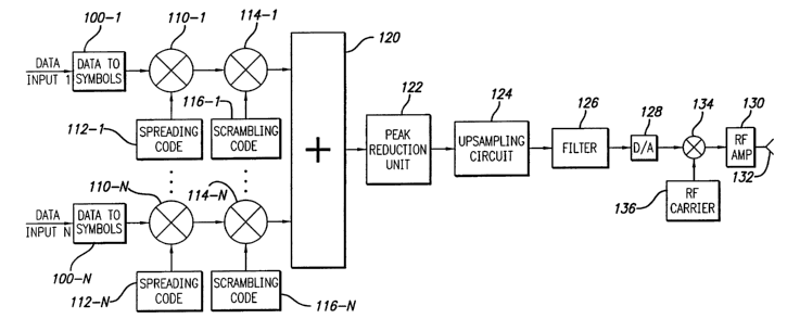
Referring to figure 6, a preferred embodiment of a spread spectrum
communication system employing peak power reduction in accordance with the
present
invention is illustrated. Although the illustrated spread spectrum
communication system
may be implemented in a wireless cellular network, such as a WCDMA or CDMA
network, and such provides one preferred application of the present invention,
it should
be appreciated that other applications and environments for the present
invention are
also possible.
As illustrated a plurality of channels, N in number, are provided as data
inputs
into the system. A data channel may comprise audio data, for example in a
digital
cellular application, or may comprise any other form of data that is desired
to be
transmitted over the communications system. The data in each channel then
passes
through a data to symbol converter 100 that provides a stream of symbols from
the
incoming stream of data bits. A variety of different symbol coding schemes may
be used
to provide the stream of symbols from the stream of incoming data bits (QPSK
or,
"Quadrature Phase Shift Keying",is used in WCDMA). (Implied in figure 6, after
the
data-to-symbol converter, all processing paths are complex and include both
ir+phase
and quadrature components.) Next, the stream of symbols in each channel is
provided
to a mixer 110 which mixes the incoming symbol stream in each channel with a
spreading code provided from a spreading code circuit 112. For example, in
spread
spectrum cellular communications systems a Walsh code can be employed. Each
channel receives a unique orthogonal spreading code which allows the
individual
channels to be recovered at the recever end by using a matching despreading
code.
After being combined with a unique spreading code each channel again may be
provided to another mixer 114 which combines the signal in each channel with a
scrambling code from scrambling code circuit 116. Tl~e scrambling code is used
in
cellular applications for cell site identification. A scrambling code is
typically employed
in cellular communications systems, but may be dispensed with in other
applications.
The output of each channel is then provided to he summing circuit 120 which
combines
the symbol streams from each of the individual channels and combines them into
a
single output symbol stream (for each of the two complex quadrature phases).
14
CA 02406757 2002-10-18
WO 01/82547 PCT/USO1/06317
Since the N channels are combined together in the summing circuit 120, the
potential of creating very large symbol peaks is presented as discussed above
in the
Background section. The present invention provides a peak reduction unit 122
thafi
reduces or eliminates signal peaks output from the filter 126 that will exceed
a given
maximum signal peak power level chosen for the particular application of the
communications system. As further illustrated in figure 6, the output of the
peak
reduction unit 122 is provided to an up-sampling circuit 124 which converts
the symbol
rate to a frequency which meets or exceeds the bandwidth requirements for the
10, frequency range of interest. Typically the up-sampling process will simply
insert zeroes
into the symbol stream to allow the signal stream to operate at the desired
higher clock
rate to meet or exceed the bandwidth requirements. Therefore, M zeroes will be
inserted
infio the symbol stream, for each incoming symbol, where M is an integer
chosen to
provide the desired up conversion. Typically the integer M will be at least 1
or greater.
The up-sampled signal stream is then provided to a filter 126. In some cases
the
operation of the up sampling circuit 124 may be incorporated in the operation
of the filter
126 rather than in a separate circuit. The filter output is providedto a
digital to analog
converter 128 that provides an analog signal. This analog signal will be made
up of in
phase and quadrature components which are not shown to this detail. This
analog
signal is mixed at mixer 134 with an RF carrier from RF source 136, which RF
modulated signal is then provided to an RF amplifier 130 and then to an RF
transmitter
132, e.g., in a wireless cellular communications base station application. The
mixer 134
in this application is in actuality a quadrature up converting miter not shown
to this
detail. As is well known to those skilled in the art the signal output from
the filter can
optionally be converted from an in-phase and quadrature signal to a real
signal offset
from the baseband center frequency of zero Hz. If this is done, the D/A
converter can
be used to create a real intermediate frequency output that can then be mixed
to an RF
frequency with a simple standard mixer.
As discussed above in the Background section, the filtering operation provided
by
filter 126 is of critical importance in many applications employing spread
spectrum
communications. (n particular, in cellular communications systems such
filtering is
critical due to the necessity to maintain the transmitted signal within a
prescribed
is
CA 02406757 2002-10-18
WO 01/82547 PCT/USO1/06317
frequency band. Also, the filter 126 will have a significant effect on the
signal peaks
produced by the symbol stream and therefore can dramatically impact any peak
reduction performed prior to such filtering.
The peak reduction unit 122 avoids this problem by predicting the filter
output 126
based on the symbol stream input and then performing a peak reduction
processing on
the symbols based on the predicted signal peak after the filtering. This
filter prediction
operation of the peak reduction unit 122 may be very accurately implemented
since the
impulse response function of the filter 126 is known in advance. Therefore,
the effect of
the filter on any given stream of symbols can be precisely predicted to any
desired
degree of accuracy by a circuit which has a desired number of filter
coefficients as
inputs to the circuit to adequately model the filter impulse response
function. These filter
coefficients are impressed on the incoming symbol stream to simulate the
effect of the
filter on the incoming symbol stream to create a predicted filtered output
stream. The
predicted filtered output stream is then subjected to a peak reduction
calculation which
determines whether the predicted filter output stream will exceed a signal
peak limit
value and if so what correction is needed. If the limit value is exceeded the
actual
symbol stream is then subjected to a peak reduction processing which reduces
the
resultanfi signal peak to the desired limit value on a symbol~by-symbol basis.
In this way, only required peak reduction is performed and minimal distortion
is
introduced into the signal. Both the accuracy of the peak reduction processing
as well as
the accuracy of the filter prediction process may be chosen based on the speed
and
complexity of the peak reduction circuitry and associated trade-offs in cost.
In most
applications, however, filter prediction processing as well as the peak
reduction
processing may be adequately implemented without adding significant
complexities or
costs to the overall system.
Referring to Figures 7 and 8 a preferred embodiment of the peak reduction unit
122.is illustrated. More specifically, a block schematic drawing of the peak
reduction unit
122 is illustrated in Figure 7 and the impulse response function for a typical
filter,
illustrating typical filter coefficients employed in the peak reduction
circuit 122, is
illustrated in Figure 8. As shown, the peak reduction unit 122 preferably
includes two
16
CA 02406757 2002-10-18
WO 01/82547 PCT/USO1/06317
stages 140,142 corresponding to peak reduction at the or~symbol interval, t =
0, and
inter-symbol interval, t = 0.5, respectively. The order of these two stages is
arbitrary. As
discussed above in relation to figure 6, the symbol stream is typically up
sampled before
passing through the filter 126. Therefore, additional sample points will be
added m
between the actual symbols in the symbol train and the filter impulse response
function
will be impressed on these added sample points as well as the symbol sample
points.
Assuming an up sampling of one added sample point for each symbol in the
symbol
stream the impulse response function of the filter will be impressed on the up
sampled
symbol stream at both the on-symbol interval and the half way position between
symbols, i.e., the inter-symbol interval. This is illustrated in figure 8
where filter
coefFcients at the on-symbol interval are illustrated by asterisks, and the
filter
coefficients at the inter-symbol interval are illustrated by crosses. Since
the effecfi of
both the symbol and inter~ymbol filter coefficients will be impressed on the
symbol
stream as it emerges from the filter 126, to accurately predict the effect of
the filter in the
peak reduction unit it is necessary to take into account both filter
coefficients at the on-
symbol interval and at the inter-symbol interval. The illustrated two-stage
process of
figure 7 allows this on-symbol and inter-symbol processing to be performed in
series.
This series implementation may use less hardware, or a less complex DSP
program,
than if the on-symbol and inter-symbol processing are done concurrently, i.e.,
in parallel.
Nonetheless, it should be appreciated that in an alternate embodiment such a
simultaneous processing could be done and such an embodiment is described
below.
Also, in the case of an up sampled symbol stream having more than one added
symbol
for each symbol in the symbol train, additional filter timing points may be
added for the
filter prediction processing. Also, it should be appreciated that it may be
possible to
provide only on-symbol (or inter-symbol) peak reduction processing and still
achieve
some beneficial results, although at least on-symbol and inter-symbol
processing is
presently preferred. In addition, any or all stages may be repeated to account
for peak
reduction errors caused by the causal nature of peak reduction processing.
Although figure 6 shows the peak reduction unit before up sampling circuit
124, it
may also be configured after the up sampling circuit (but before the filter
126). When
operating after up sampling, coefficients are taken directly from the filter
impulse
response function at the up sampled rate. These coefficients are then used to
create a
W
CA 02406757 2002-10-18
WO 01/82547 PCT/USO1/06317
filter output predictor. Filter output predictions will then be made at the up
sampled rate.
From these predictions, peak reductions would be made. Thisapproach is not
preferred
for certain applications and/or certain impulse response functions. When
operating at
the up sampled rate, peak reductions may be provided to the zero value symbols
added
during up sampling. Digital communication systems such as CDMA and WCDMA use
transmit and receive filters designed to minimize inter-symbol interference.
To maintain
minimum inter-symbol interference during communication, the zero valued
symbols
added during up sampling must remain zero valued. Also, operating at the up
sampled
rate requires processing to be performed at that higher rate. Generally, the
higher the
processing rate, the more expensive the processing components cost. There may
be
applications however, where these costs are trivial and need not be considered
and
processing after up sampling is preferred. Any modifications necessary for the
below
described specific embodiments to implement the peak reduction unit after up
sampling
will be apparent to those skilled in the art and are implied heren.
Both stages of figure 7 can use the reduction process shown in figure 9.
Referring to figure 9, the reduction process includes a source 144 of the
filter
coefficients. These filter coefficients are taken from the filter impulse
response function
at either the on-symbol or inter-symbol interval depending on the processing
stage 140
or 142 of figure 7. The source of these coefficients may take the form of a
memory 144
storing the filter coefficients, e.g., the coefficients illustrated in figure
8 for the
appropriate symbol interval. Of course, other filter implementations may have
differing
filter response functions and therefore different filter coefficients will be
stored in the filter
coefficients memory 144. These filter coefficients are provided to a filter
predictor 146,
which receives the incoming symbol stream provided along line 148 and
simulates the
effect of filter 126 on the symbol stream at the chosen symbol interval. Two
outputs are
provided from the filter predictor. One output 147 is a filter coefficient
weighted sum
using ail input filter coefficients and an equal number of time differentiated
input
symbols. The other output 145 is a filter coefficient weighted sum where only
the center
filter coefficients and matching centered symbols are used. When an odd number
of
filter coefficients are used, the second output is the center coefficient and
the matching
center symbol used to calculate the first output 147. When an even number of
coefficients are used, the two center coefficients will have the same value
and may be
is
CA 02406757 2002-10-18
WO 01/82547 PCT/USO1/06317
used along with both matching center symbols used to calculate the first
output 147.
Each time a new symbol enters the filter predictor both outputs are generated
by 146.
Each new output pair is provided on a symbol-by-symbol basis, to a peak
reduction
algorithm processing circuit 152. The peak reduction algorithm processing
circuit 152
compares the magnitude of the first predicted filter output 147 to a
predetermined
maximum allowable peak limit value L. If the first predicted filter output 147
exceeds the
limit value then the peak reduction algorithm circuit 152 calculates an
adjusfiment to the
second filter predictor output 145 which will result in a filter output which
will remain
within the peak limit value after processing by filter 126 of figure 6. This
adjustment is
then applied to the corresponding symbols, delayed by delay circuit 166, on a
symbol-
by-symbol basis by combiner 168. The peak adjusted symbol stream is then
output
along line 154. A variety of different algorithms may be employed in the peak
reduction
algorithm circuit 152. The specific algorithm chosen may be based on the
desired
degree of accuracy and the available processing speed andlor complexity of
hardware
desired for the specific application. For example, in many applications an
approximate
algorithm may be perfectly acceptable and give the desired peak reduction in
the symbol
train
An alternate embodiment of figure 9 is shown in figure 10 where the filter
predictor 146, the delay 166, and the combiner 168 of figure 9 are
incorporated as part
of the filter predictor. Adjustments provided by the peak reduction algorithm
152 are
then fed back into the filter predictor to incorporate present adjustments on
future
predictions. This incorporation will be discussed in greater detail when
filter predictor
embodiments are discussed.
Referring to figure 11, an alternate embodiment of the peak reduction unit 122
(of
figure 6) is illustrated. The implementation of figure 11 provides a
multistage peak
reduction unit with the series arrangement of the multiple stages.
More specifically, referring to figure 11 the illustrated peak reduction unit
includes
a plurality of individual stages 320. Each stage 320 in the peak reduction
unit applies a
filter prediction operation using a set of periodically sampled filter
coefficients
corresponding to a particular filter output timing. For example, if the up
sampling inserts
19
CA 02406757 2002-10-18
WO 01/82547 PCT/USO1/06317
9 zeros between symbols then the actual filter operation which occurs will
include 10
filter timing points for each symbol interval. To provide a perfectly accurate
model of the
filter operation each of these filter timing points would need to be included
in peak
reduction processing. Thus, the filter impulse response function would need to
be
sampled at 10 different locations for each symbol interval. This example of 10
filter
coefficient sampling positions for each symbol interval is illustrated for a
specific impulse
response function in figures 12- 21. Each of these 10 figures illustrates
different filter
coefficient sample timing within symbol interval. In particular, figure 12
indicates a
sampling of the impulse response function periodically at the symbol interval
starting at
a timing of -0.5 from the on-symbol interval, i.e., the halfway point between
two symbols
offset in the negative time direction (inter-symbol). Figure 13 illustrates
the impulse
response function sampled periodically at the symbol interval starting from a
timing of-
0.4. Figures 14 - 21 in turn illustrate consecutive sample timing offsets from
-0.3 --
~-0.4. Figures 12-21 thus cumulatively represent 10 filter coefficient sample
locations
symmetrically about the on-symbol interval. Each stage 320 of the peak
reduction unit
of figure 11 implements a filter prediction operation at an individual sample
timing point.
Therefore, for the specific impulse response function and sampling illustrated
in figures
12 - 21, ten separate filter stages 320 would be provided each providing the
filter
prediction operation at one timing point corresponding to one of figures 12 -
21.
Specifically, stage 320 -1 may correspond to the sample timing illustrated in
figure 12,
stage 320 --2 to the sample timing illustrated in figure 13, etc.
It will of course be appreciated that the example of 10 sample points and 10
stages in figure 11 and figures 121 is purely illustrative and a greater or
lesser
number of sample points and stages may be provided. Also, the number of stages
320
need not correspond to the specific amount of up sampling occurring and fewer
stages
and coefficient sample points may be employed than the actual amounfi of up
sampling
points. Also, figure 11 shows each peak reduction process arranged in time
order from t
- -0.5 to t = 0.4. The time relationship of the peak reduction stages in
figure 11 can be
in any arbitrary order. In addition, any or all stages may be repeated to
account for peak
reduction errors caused by the causal nature of peak reduction processing.
Referring to figure 22, an alternate embodiment of the peak reduction unit is
CA 02406757 2002-10-18
WO 01/82547 PCT/USO1/06317
illustrated which includes a multi-stage peak reduction processing implemented
in a
parallel manner. The embodiment of the peak reduction unit described above in
relation
to figure 11 implemented a multi-stage peak reduction process in a series
manner. In
the embodiment illustrated in figure 22, a similar multi-stage peak reduction
process is
implemented in parallel. That is, each stage 360 illustrated in figure 22
implements a
peak production processing based on different timings of the filter
coefficients of the filter
impulse response function corresponding to a higher rate filtering occurring
after up
sampling of the input symbols. For example, each stage 360 illustrated
in~figure 22 may
perform a peak reduction processing employing filter coefficients sampled at
the
IO different timings shown in figures 12 - 21. As in the case of the
embodiment of figure
11, however, different timings and different specific filter impulse response
functions
may be employed and the specific filter coefficients and coefficient sample
timings of
figures 12 - 21 are purely illustrative. In addition, any or all symbol
coefficient timings
may be repeated to account for peak reduction errors caused by the causal
nature of
peak reduction processing.
In the embodiment of figure 11 described previously, each subsequent stage in
the multi-stage peak reduction unit receives as an input thereto the already
peak
adjusted symbols from the preceding stage. Therefore, unnecessary duplication
of peak
adjustment to symbols previously adjusted is avoided by this series
implementation. In
the parallel implementation of figure 22, preferably a multi-stage feedback
approach is
employed which feeds back peak reduction values from the parallel peak
reduction
stages into the other stages to achieve a similar result. More specifically,
the peak
reduction process of the top branch, branch 0, of figure 22 receives feedback
from its
own internal peak reduction algorithm and also provides this feedback to all
lower
branches. Lower branches, like branch i, receives feedback from its own
internal peak
reduction algorithm and feedback from all branches above it. The last branch,
branch
N-1, receives feedback from all branches including its own internal peak
reduction
algorithm. The bottom stage outputs the fully peak adjusted symbol stream as
illustrated in figure 22.
Referring to Figure 23, an alternate to the parallel processing embodiment is
shown. This embodiment is identical to that of figure 22 except feedback from
all
21
CA 02406757 2002-10-18
WO 01/82547 PCT/USO1/06317
branches is provided to the peak reduction units of each branch. This
alternate
embodiment improves peak reduction calculations from each branch since each
calculation will be based on the most currently adjusted symbols.
Since the peak reduction processing is done in parallel in the embodiments of
figures 22 and 23 it may be done faster than the series implementation
described
previously. Therefore the implementation of figures 22 and 23 may be preferred
in some
situations. Also, since the processing can be done faster it may be possible
to perform
filter predictions at more coefficient timings and/or using more coefficients
thereby
increasing the accuracy of the peak reduction processing using the parallel
implementation of figure 22.
Referring to figure 24, one stage 360 of the parallel peak reduction unit of
figures
22 and 23 is illustrated. As shown, the input symbols to the stage 360 are
first provided
to filter predictor 372 which performs a filter prediction processing
employing filter
coefficients at a specific offset-symbol timing, illustrated as provided from
filter
coefficient supply 144. Filter coefficient supply 144 may be hardwired into
the circuitry
or may take the form of a suitable memory such as a register in a suitably
programmed
DSP implementation of the peak reduction unit. As noted above, the specific
sample
offset timing for the filter coefficients supplied to the filter predictor 372
correspond to
selected sample offset timings at the up sampled rate of the actual filter
employed in the
system. Thus, for example, sample timings such as illustrated in figures 12-
21 may be
employed for the filter coefficients stored in filter coefficients supply 144
for each specific
stage 360.
The filter predictor 372 outputs the two predicted filtered outputs described
in
figure 9, to the peak reduction algorithm circuit 152 which implements a
suitable peak
reduction algorithm to determine a peak reduction value, if necessary, to
reduce the
peak to a desired limit value. The calculated peak reduction value is output
from stage
360 as a feedback value F; which is provided to its own internal filter
predictor 372 and
to the filter predictors of other parallel branches 360-I of figures 22 and
23.
As noted above a variety of different algorithms may be implemented in the
peak
22
CA 02406757 2002-10-18
WO 01/82547 PCT/USO1/06317
reduction algorithm circuit 152 of figures 9, 10, and 24. One such algorithm
is illustrated
in figure 25. Figure 25 shows a complex vector diagram illustrating the filter
output
based on a filter coefficient weighted sum of input symbols using all input
coefficients
and a filter coefficient weighted sum of input symbols where only the center
filter
coefficients and matching centered symbols are used. From these two inputs a
correction value is calculated for the filter centered symbols suitable to
place the filter
output within the preset limit value L. The algorithm illustrated in figure 25
was
specifically designed to induce only amplitude errors to the input symbols.
Some
communication systems are more tolerant to amplitude errors than phase errors.
More specifically referring to figure 25, the output of the filter based on
the center
input symbols is illustrated by vector A. The predicted filter output based on
multiple
input symbols, including the centerinput symbols, is indicated by vector B.
The vector D
is calculated by taking the difference of these two vectors. Vector D
therefore
represents the multi-symbol output from the filter with the center symbol
vector A
missing. The output gA represents a gain adjusted version of vector A which
when
added to D pulls the filter output back to the limit level L. The remaining
vectors shown
in figure 25 are used to calculate the gain g. The gain g is calculated by the
following
series of vector computations.
L2 =z2 +y2
z = L2 -- y 2
gIAI- L2_Y~ _x
_ D~A
x IAI
Y = D _ CD . A~A
IAI2
2
g= L2- p_(D'A~A ~(D~A~ 1 (1)
IAI IAI IAI
23
CA 02406757 2002-10-18
WO 01/82547 PCT/USO1/06317
This algorithm may be implemented in peak reduction algorithm circuits shown
in
figures 9, 10 and 24 through use of a suitably programmed DSP or other
processor.
Since the algorithm involves taking a square root of vector quantities it can
be somewhat
calculation intensive and therefore it may be desirable to employ an
approximate
algorithm which nonetheless will provide adequate symbol correction in most
cases. In
particular, if it is assumed that the difference between the predicted output
B and the
single symbol output A is relatively small, i.e. D in the above equation is
small. The
following approximate formula can be used to calculate the gain g needed to
reduce the
filter output to the limit value L.
L + IAI - IBI
g ~ IAI , for small 'D' (2)
The value of gain calculated using the above exactor approximate algorithm is
then applied to the combiner 168 illustrated in figure 9. The combiner may
simply be a
multiplier circuit which multiplies the gain g and the input symbol which
produced the
I5 output vector A. Alternatively, the combiner may be changed to a summing
circuit if the
gain calculations found in (1) and (2) above are converted to a vector
adjustment
provided through equation (3) below. The value gcis the gain applied by the
filter on the
center symbols which produced vector A in figure 25.
V = (A - gA~ g c (3)
As noted above, a variety of different algorithms may be used to calculate the
symbol adjustment that places the predicted filter output within the limit
value L. One
such additional algorithm is illustrated in relatirn to figure 26 which shows
the calculation
of a correction vector that is combined with the center input symbols through
addition.
The algorithm differs from that of Figure 25 in that the adjustment permits
phase errors
in order to minimize the total distortion energy added. More particularly, as
illustrated in
figure 26 the vectors A, B, and D have the same meaning as in relation to
figure 25. In
figure 26 the value C is the additive adjustment made to the predicted filter
output to
place it at the limit value L. Although a variety of adjustment vectors could
be added to
place the resulting vector at the limit value L, it is desirable to minimize
the size of the
24
CA 02406757 2002-10-18
WO 01/82547 PCT/USO1/06317
vector C and hence the amount of correction since any changes made to the
input
symbols potentially result in some distortion in the signal. Applying basic
vector algebra
to the vectors illustrated in figure 26 results in the following equation to
determine the
correction C to be applied to the center symbol filter output A to get the
desired peg
reduced output within the limit value L:
C - L ~B~ _ B . (4)
Before addition with the symbol adjustment, the above vector must be gain
adjusted by the inverse.filter gain applied to the center symbols used to
calculate the
vector C. The resulting algorithm for adjusting symbols for peak reduction is
given in
(5). This algorithm may be implemented in a suitably programmed DSP or other
hardware or software implemented circuitry.
V = L B -B ~ (5)
gc
The value of the correction vector calculated in equation (5) above is then
applied
to the combiner 168 illustrated in figure 9. The combiner may simply be an
addition
circuit which adds the vector V to the center symbols which produced the
outprt vector
A. Alternatively, the combiner may be changed to a multiplier circuit if the
vector
calculation found in (4) is converted to a gain adjustment provided through
equation (6)
below.
g = (A + C) A (6)
It should be appreciated by those skilled in the art that the two algorithms
illustrated in figures 25 and 26, respectively, are purely illustrative in
nature'and a variety
of different algorithms may suitably be employed and may be implemented in a
DSP or
other circuitry comprising peak reduction algorithm circuit 152 illustrated in
figures 9, 10,
and 24.
CA 02406757 2002-10-18
WO 01/82547 PCT/USO1/06317
Referring to figures 27 and 28, examples of the peak reduction processing in
accordance with the present invention are illustrated in two complex vector
diagrams.
Figures 27 and 28 apply to the case where only one center symbol is adjusted.
The
input symbol shown could however represent the combination of two center
symbols.
As shown in figures 27 and 28, input symbols are provided with filter
predictor
processing. Since the output of the filter is dependent on many symbols in
time, not just
the center symbol to be adjusted, the output can be represented as the center
symbol
and circle representing the affect of symbols neighboring in time.
Although the center symbol exceeds the lirrit value initially in both
examples, in
the example of figure 27 a portion of the circle representing the filtered
outputs actually
lies within the limit line. These output values are therefore not subject to
peak reduction
processing. The remainder of the outputs, illustrated in bold in the complex
diagrams of
figures 27 and 28, are subject to peak reduction processing by an amount
varying with
the extent the filtered symbol exceeds the limit line. The symbols are then
adjusted so
the predicted filter output is pulled back to the limit line, as illustrated
by the bold portion
of the limit line in figures 27 and 28. Therefore, it will be appreciated that
symbols not
requiring peak limit processing are left untouched, thereby reducing any
distortion
introduced via such reduction, but also symbols which do require peak
reduction
processing are provided the minimum amount of peak reduction necessary to
place the
filtered outputs within the limit value. Conversely, symbols that may
initially not appear
to require peak reduction processing will be peak adjusted if the filter
prediction shows
that the filter output will exceed the limit value. Accordingly, it will be
appreciated that
the present invention provides highly effective signal peak reduction while at
same time
minimizing distortion introduced into the symbol train.
Figures 29 through 35 show different embodiments of peak reduction units using
the algorithms given in equations (1), (2), (3), (5), and (6). Figures 29, 30,
32, and 34
represent the peak reduction processing shown in Figure 9. Figures 31, 33, and
35
represent the reduction processing shown in Figure 10. An example of the
parallel
processing shown in figures 23 and 24 will be given in figure 36A and 36B.
26
CA 02406757 2002-10-18
WO 01/82547 PCT/USO1/06317
Referring to figure 29, an embodiment of the peak reduction unit using
equation
(1) is illustrated in a block schematic drawing. As shown in figure 29,
employing a multi-
tap filter 200 may advantageously combine the delay circuit 166 and the filter
predictor
circuit 146 shown in figure 9. The filter 200 includes a plurality of
individual memory
registers 202 of which 5 are illustrated in the specific embodiment of figure
29. It should
be appreciated however that additional or fewer delay memory registers may be
provided and in general N such memory registers 202 will be provided forming
an N
element shift register. By tapping a memory register output, e.g., at the
center memory
IO register, a delayed symbol train may be provided so that the peak
correction can be
done on a correctly timed symbol-by-symbol basis at the combiner 168. Such a
delayed
output from the N element memory registers is illustrated by line 205 and thus
corresponds to the output of the delay circuit 166 illustrated in figure 9.
The output
provided along line 204 is derived from a tap of the center delay stage after
multiplication with the center filter coefficient. This line represents the
center filtered
symbol output (line 145 in figure 9 and vector A in figure 25) which is
provided to the
peak reduction algorithm processing circuit 152 as shown in figure 29. The
delayed
outputs from each of the memory registers 202 are provided to a corresponding
multiplier 206 .which also receives a corresponding filter coefficient as an
input thereto.
Each filter coefficient thus acts as a gain gN, N=1 to 5, multiplying the
symbol output
from the corresponding delay stage 202. The filter coefficients g.~ may
correspond to
any of symbol interval coefficients illustrated in figure 8 or figures 12- 21
depending on
which stage in the processing of figures 9 or 11 is represented. Of course, a
variety of
different filter response functions may be used depending on the particular
filter being
predicted and the coefficients will vary accordingly. Also, it will be
appreciated that
additional coefficients may be taken at any symbol interval from the impulse
response
function with the example of five coefficients being purely illustrative in
nature, and more
or less than five coefficients may be employed for the particular
implementation,
depending on the specific impulse response function being modeled as well as
the
speed of the processing system employed and the desired accuracy.
Still referring to figure 29, the outputs from the multiplier circuits 206 are
provided
to summing circuit 208 which sums the plural outputs and provides them along
line 210.
27
CA 02406757 2002-10-18
WO 01/82547 PCT/USO1/06317
The output along line 210 corresponds to a filter coefficient weighted sum of
symbols
taken at a specific symbol interval and thus corresponds to a model of the
filter impact
on the symbols at that interval. This predicted filter symbol output is
provided along line
210 as an input to the peak reduction algorithm circuit 152. The peak
reduction
algorithm circuit 152 also receives the delayed center symbol filter output
along line 204
as noted above. This delayed center symbol filter output stream is provided
along line
212 to a subtraction circuit 216, and along line 214, to algorithm processor
218.
Subtraction circuit 216 thus receives the filtered outputs provided along line
210 as one
input thereto and the delayed center symbol filter outputs along line 212 as a
second
input thereto. Subtraction circuit 216 takes the difference these two output
streams,
providing a symbol-by symbol difference value D (D=&A using the terminology of
figure
25) along line 220 to algorithm processor 218. The algorithm processor 218,
which
receives the two input symbol streams along line 220 and 214, also receives
the limit
value L as input. The algorithm processor 218 computes the gain g using
equafiion (1)
to reduce the filtered outputs to a value lying within the limit value L.
In a more general case the subtraction circuit 216 would be combined with the
algorithm processor 218 to create a more general-purpose algorithm processor.
With
this minor modification to figure 29 a variety of different algorithms could
be used based
on the inputs from lines 204, 210 and the limit value L. In this more
generalpurpose
case either the approximate algorithm given in equation (2) or algorithm based
on figure
26, given in equation (6), could be used.
In either the specific case shown in figure 29 or in the more general-purpose
case
described, the computed gain value g from the algorithm processor 218 is
output along
line 232 to selection switch 230.
Still referring fio figure 29, the filtered output stream provided along line
210 is
also provided to magnitude detection circuit 222. The magnitude defection
circuit 222
determines the magnitude of the filtered outputs, i.e., the absolute value of
the complex
vector quantity comprising the outputs, which magnitude is provided as an
output along
line 224. This magnitude is provided to comparator 226 which compares the
magnitude
of fihe filtered symbols to the limit value L. If the magnitude of the
filtered symbol
28
CA 02406757 2002-10-18
WO 01/82547 PCT/USO1/06317
exceeds the limit value L the output from the comparator 226 takes a first
value (e.g.,
"1"). If the magnitude of the filtered symbol is less than the limit value L
then the output
from the comparator 226 is a second value (e.g., "0"). This value, i.e. a "0"
or "1", is then
provided as an output along line 228 to selection switch 230. If the input to
the selection
switch 230 along line 228 is a 0, then the output from the selection switch
230 is a unit
signal which has no affect on the symbol stream provided abng line 205 to
combiner
168 (illustrated as a multiplier in the specific embodiment of figure 29). If
the signal
provided along ~ line 228 to selection switch 230 is a one, corresponding to
the filtered
symbol value exceeding the limit value L, then the conputed gain value g
provided from
algorithm processor 218 is output to multiplier 168. In this way the symbol
stream
provided along line 205 wi(I be gain reduced by the appropriate value computed
by the
algorithm only it necessary on a symbol-by-symbol basis and appropriately peak
adjusted symbols will be output on line 154.
It will be appreciated that the various circuit elements illustrated in figure
29 may
be implemented solely in hardware, solely in software, i.e., as a suitably
programmed
DSP or other processor, or may be implemented as a combination of hardware and
software. For example, it may be advantageous for the filter 200 to be
implemented as
hardware whereas the algorithm processor 218 is implemented as a suitably
coded DSP
processor. Alternatively, the circuitry of algorithm processor 218 may be
implemented
as a programmable gate array circuit. Also, filter 200 andlor difference
circuit 216 and
magnitude detector 222 may be implemented as a gate array circuit and combined
with
a processor based circuit 218. Therefore, it will be appreciated that a
variety of different
combinations of implementations of the circuitry illustrated in figure 29 are
possible.
Referring to figure 30, an alternate embodiment of the peak reduction unit
shown
in figure 29 is illustrated. In the embodiment of figure 30, the peak
reduction algorithm is
implemented in a simplified peak reduction algorithm circuit 152 that utilizes
an
approximate equation for the peak reduction to be applied to the input
symbols. In
particular, the specific embodiment illustrated in figure 30 may implement the
equation
(2) described above that provides an approximate calculation for the gain g
applied to
the symbol vector to bring it to the limit value L.
29
CA 02406757 2002-10-18
WO 01/82547 PCT/USO1/06317
As may be seen, the equation involves relatively simple calculations involving
the
limit value L, the magnitude of the center symbol filter output A, and the
magnitude of
the predicted filtered output B. Comparing this equation to the circuitry of
peak
reduction algorithm circuit 152 illustrated in figure 30 shows that circuit
222, 250, 252,
254 and 256 implement equation (2) in a straightforward manner. More
specifically, line
204 along with the magnitude detection circuit 250 provides the magnitude of
the center
symbol filter output A. The predicted filtered output is provided from filter
200 to
magnitude detection circuit 222 which determines the magnitude of the
predicted filtered
output B. These two magnitudes are provided to subtraction circuit 252, which
performs
a subtraction of the symbol magnitudes to provide the value ~A~- ~B ~ . Adder
circuit 254
(which may be a subtraction circuit if circuit 252 interchanges its inputs)
then adds this
value provided from circuit 252 to the limit value L. The center filtered
output provided
from circuit 250 is provided to division circuit 256 which also receives the
output of
circuit 254 to provide the approximate peak reduction gain g given by the
above
equation (2).
It will therefore be appreciated that the circuit implementation illustrated
in figure
30 for the peak reduction algorithm circuit 152 provides a relatively simple
implementation that may be easily provided in hardware. This hardware may take
the
form a programmable gate array or other hardware implementation, or in a
relatively
simple program implemented in a DSP or other processor. This relative
simplicity of the
implementation shown in figure 30 can have cost and/or speed advantages and
may be
preferred in particular applications. The remainder of the circuitry in the
embodiment
illustrated in figure 30 may be precisely the same as illustrated in figure
29, and may
operate in exactly the same manner as described above. Therefore, the
operation of
this common circuitry will not be repeated for describing the embodiment of
figure 30.
Referring to figure 31, an alternate embodiment of the peak reduction unit is
illustrated. The embodiment of figure 31 employs feedback from the output of
the peak
reduction algorithm circuit 152 to the filter predictor to increase the
accuracy of the filter
prediction operation. Figure 31 therefore represents one embodiment of figure
10. More
specifically, as in the previously described embodiments, the filter predictor
and the
delay circuit are preferably combined in a finite element filter 200 which
incorporates a
CA 02406757 2002-10-18
WO 01/82547 PCT/USO1/06317
plurality of memory registers 202 which receive the input symbols and operate
as an N
element shift register. As in the case of the embodiment of figure 29, the
output of the
memory registers are provided to multiplier circuits 206 which also receive
the filter
coefficients as inputs thereto. The multiplier outputs are provided to adder
circuit 208 to
provide the filtered output symbols also as in the case of the embodiment of
figure 29.
The peak reduction algorithm circuit 152 illustrated in figure 31 also
corresponds to that
in figure 29, however, it may be modified to implement a variety of different
algorithms
as has been discussed above in relation to previous embodiments.
In contrast to the embodiment of figure 29, in figure 31 the output of the
peak
reduction algorithm circuit 152 is fed back to the filter 200. In particular,
the output of the
peak reduction algorithm circuit 152 is provided back along line 262 to a
multiplier 168
which provides the peak reduction gain calculated by the circuit 152 to the
output of the
center delay stage of the N stage memory registers of filter 200. As a result,
the output
of the multiplier 168 provided to the downstream stages of the memory
registers
includes the already gain reduced symbol values. This will more accurately
reflect the
actual processing by the filter 126 (referring to figure 6) since the gain
reduced symbols
will be included in the computation of the filtered symbol by filter 200.
Therefore, the
embodiment illustrated in figure 31 may in many cases provide a more accurate
filter
prediction and may be preferred in some applications.
A similar feedback extension can be made to the embodiment shown in figure 30
where equation (2) is specifically defined by a unique black diagram. This
extension
should be easily understood by those skilled in the art.
As stated above, the feedback modification provides an adjusted symbol for all
following peak adjustment calculations. Prior to modification however, the
preadjusted
symbol was used to calculate peak adjustments preceding the adjustment time.
This
means that when the adjusted symbol stream is passed through the filter (20 in
figure 6)
the adjusted symbol will participate in creating peaks both preceding and
following the
adjusted symbol. New peaks therefore can be created preceding the adjusted
symbol.
These new peaks are the result of the causal or non-anticipatory nature of the
peak
adjustment process. Simply repeating each stage in the peak reduction
processes
31
CA 02406757 2002-10-18
WO 01/82547 PCT/USO1/06317
shown in figures 7, 11, 22 and 23 can easily eliminate these new peaks.
Previous embodiments described symbol adjustments based on gain corrections
that can be calculated from equations (1), (2) and (6). Symbol adjustments can
also be
S base on adding vectors that can be calculated from equations (3) and (5).
Referring to
figure 32, one embodiment that adjusts symbols based on adding vectors is
illustrated.
In the embodiment of figure 32 the delay circuit 166 of figure 9 is
implemented as part of
a series of memory registers forming part of the filter predictor circuit 146
in a similar
manner to embodiments described previously. More specifically, filter 200
includes a
plurality of the memory registers 202 which may operate as an N element shift
register,
the specific illustration being a 7 element shift register. The output of the
center stage of
the memory registers is tapped as an output to provide the delayed symbols
along line
205 to combiner 168. Combiner 168 is illustrated as an adder circuit. The
outfit of the
memory register stages are provided to multiplier circuits 206 which also
receive as
1S inputs thereto filter coefficient values at the particular symbol timing
corresponding to
that stage. The outputs of the multipliers 206 are provided to summing circuit
208 which
outputs a predicted filter output value along line 210, similarly to
previously described
embodiments.
The predicted filter outputs along line 210 are provided to the peak reduction
algorithm circuit 218 which implements a particular peak reduction algorithm
on the
predicted filter outputs and provides the reduction value, if any, to combiner
168. In the
embodiment of figure 32 a particularly simple algorithm may be implemented
thafi does
not require an input from the center filtered symbol output along line 204 but
simply
2S operates on the predicted filter outputs provided along line 210. The
algorithm also
employs as input the desired limit value L and the gain of the center tap of
the filter
predictor, g4 for the particular embodiment shown. Such an algorithm may
correspond to
equation (5) described above in relation to figure 26. Other algorithms
however, may
also be employed within circuit 338. Such other algorithms may require an
input from the
symbol stream provided along line 204 and the possibility of such an input to
circuit 152
in figure 32 is understood in the case of such alternate embodiments. Just
such an
algorithm is given in equation (3) where the value g in equation (3) is
calculated in
equation (1).
32
CA 02406757 2002-10-18
WO 01/82547 PCT/USO1/06317
In the illustrated embodiment of the circuit 152, the magnitude of the
predicted
filter outputs provided along line 210 is determined by magnitude detection
circuit 222.
This is provided to a comparator 226 which compares the magnitude of the
predicted
filter output values to the threshold L. The predicted filter outputs are also
provided to
algorithm processor circuit 218 which may be a suitably programmed DSP or
other
processor which implements equation for the particular embodiment shown or
other
suitable algorithm which operates on the predicted symbols. Alternatively, the
algorithm
processor 218 may be implemented in a gate array structure or other hardware
implementation. The output from the algorithm processor 218 is provided to
selector
switch 230 that also receives the output of the comparator 226. If the
predicted symbol
value is greater than the threshold value L then the output from the
comparator enables
the switch 230 to output the peak correction value to combiner 168. On the
other hand if
the predicted symbol value is less than or equal to the limit value L then the
output of the
comparator to the selector switch 230 selects a zero output to the combiner
168
corresponding to no peak adjustment to the symbol stream.
Referring to figure 33, an alternate embodiment of figure 32 is illustrated
employing a feedback of the peak adjustment to the filter predictor as given
in figure 10.
More specifically, in the embodiment of figure 33, filter 200 receives a fed
back peak
adjustment value from the peak reduction algorithm circuit 218 along line 262.
Filter 200
illustrated in figure 33 may correspond to an N stage implementation as in the
case of
figure 32 and therefore need not be described in detail. As illustrated the
peak value
adjustment provided along line262 may be provided to a combiner 168,
illustrated as an
adder in figure 33, configured after the center stage of the memory register
forming part
of filter 200. Therefore, the peak adjustments to the symbols are included in
the
subsequent stages of the filter providing an additional improvement in the
prediction
capability of the filter 200. It will be appreciated that different filter
implementations may
be advantageously implemented with differing feedback locations in the memory
registers therein. Therefore, the specific implementation shown in figure 33
is purely
illustrative and should not be taken as limiting in nature.
Referring to figure 34, a block schematic drawing of an alternate embodiment
of
33
CA 02406757 2002-10-18
WO 01/82547 PCT/USO1/06317
the peak reduction circuit unit of figure 29 is ilustrated. To understand the
justification
for this alternate embodiment, remember that inter-symbol peaks are dominated
by two
adjacent similar amplitude symbols. This was described above in reference to
figure 4.
If just on-symbol and inter-symbol adjustments are made, there will be a
significant
number of similar amplitude symbols after on symbol processing. Figure 34
substantially corresponds to figure 29 except the delay is one element longer
and the
two adjacent symbols centered in the filter predictor memory registers are
adjusted.
Both center coefficients have the same value.
The implementation of the circuit shown in figure 34 substantially corresponds
to
that of figure 29 and accordingly like numerals are employed for like
components,
therefore the specific description of each component will not be repeated. As
discussed
above in relation to figure 29, the circuit operates to predict the filter
impulse response
effect on the input symbols at the inter-symbol interval, using a multi-tap
fiter 200, and
provide peak reduction processing based thereon. Filter 200 corresponds
generally to
filter 200 in figure 29 with the following modifications. The inputs gN, N=1
to 6, to the
multipliers 206 are selected from the inter-symbol interval filter
a~efficients (t = 0.5), as
illustrated by the crosses in figure 8 for the particular impulse response
function shown
there. As discussed in relation to figure 29, the particular filter
coefficients are purely
illustrative in nature in figure 8 and so the inputs g,~ are not limited to
the specific inter-
symbol values shown there. To provide symbol correction to the two symbols
dominantly
responsible for inter-symbol peaks, a filter output from both center filter
taps 202-3 and
202-4 is provided to a summing circuit 240 to create line 204. The line 204 is
equivalent to the single symbol filter output A shown in figures 25 and 26.
The peak
adjustment is then processed as before with the gain correction applied to
both center
taps through the use of a single dement memory register 244 and multiplier
242.
Accordingly, it will be appreciated that the output symbol stream on line 154
provides a
properly peak adjusted symbol stream adjusted on a symbol-bysymbol basis at
the
inter-symbol interval but otherwise in the same manner as discussed in
relation to figure
29. Although the processing is thus preferably the same in figure 34 as in
figure 29, in
some circumstances it may be desirable to implement a different algorithm in
figure 34
from figure 29 or otherwise modify the processing at the inter-symbol interval
from the
on-symbol interval.
34
CA 02406757 2002-10-18
WO 01/82547 PCT/USO1/06317
Referring to figure 35 an alternate embodiment of figure 34 that also employs
feedback in a manner described in relation to figure 31 is shown. More
specifically, as
shown in figure 35 the filter 200 includes a feedback from the peak reduction
algorithm
circuit 152. This feedback loop provides the gain g for peak reduction
calculated by the
peak reduction algorithm circuit 152 along line 262 to the N stage memory
registers
forming part of filter 200. In the particular embodiment illustrated, this fed
back gain is
provided to multiplier 168-1 and multiplier 168-2 on opposite sides of the
fourth memory
register. This introduces the symbol gain to both symbols most responsible d
inter-
symbol peaks. This implementation is based on the specific inter-symbol
impulse
response function of figure 8 and the specific choice of filter delay stages.
Therefore, it
will be appreciated that a different introduction of the fed back gain into
the memory
register stages may be provided in a different filter implementation or for a
different
impulse response function. The output of the stage reduction process is
provided from
the last stage of the memory registers along line 154 as illustrated. As in
the case of the
embodiment of figure 31, the feed back of symbol reduction into the memory
registers
can improve the prediction capability of the filter 200 and may be preferred
in some
cases.
Figures 34 and 35 describe alternate embodiments to figures 29 and 31. Similar
alternate embodiments can be made to figures 30 and 32. These alternate
embodiments should be apparent to those skilled in the art from the foregoing
explanation.
Referring to figures 36A and 36B, a detailed implementation of theparallel
multi-
stage peak reduction unit of figure 23 is illustrated. The particular
implementation
shown in figure 36A includes 10 parallel peak reduction processing stages. It
will be
appreciated, however, that this is purely illustrative and a greatff or lesser
number of
stages may be employed depending on the particular application. Also as
previously
mentioned, peaks caused by the causal nature of peak reduction can be removed
by
repeating stages. In parallel processing this repetition is perform~l by
continuing the
periodic sampling of the impulse response function performed in figures 12
through 21
which represent periodic samplings taken a-0.5 to 0.4. Samples taken at t =
0.5, will be
CA 02406757 2002-10-18
WO 01/82547 PCT/USO1/06317
identical to samples taken at t = -0.4. This duplication of the sampling
patterns will
continue over the interval t = -0.5 to 0.5. These repeated samplings can then
be added
to the bottom of figure 36A as parallel lines 10, 11, etc.
Each stage includes a delay circuit 370 which as shown may be implemented as
a sequence of memory registers 378 each one of which delays the symbol stream
by a
time corresponding to the time between symbols. As before, taps are taken from
these
memory registers to calculate a filter coefficient weighted sum of symbols
stored in the
memory registers. As shown in figure 36A an additional delay memory register
must be
added to successive parallel stages. These delay registers allow for proper
timing of the
feedback symbol adjustments from the parallel stages.
The individual taps from each parallel delay stage T;,", i= 0 to 10, N = 0 to
7, are
provided to a filter predictor 200 which provides outputs to multipliers 206
(referring to
figure 36B, the filter predictor for the i-th stage is illustrated) which
receive as second
inputs thereto the individual fitter coefficients g;,". The outputs of the
multipliers 206 are
provided to the summing circuit 208 which provides the filter coefficient
weighted sum of ,
the symbols stored in the memory registers. The output along line 210
therefore
represents a prediction of the filter output (126 of figure 6) at the timing
associated to the
present filter coefficients g,".
The output of the filter predictor 200 provided along line 210 is provided to
peak
reduction algorithm calculation circus 218. In the particular implementation
shown, the
peak reduction algorithm calculator circuit includes a magnitude detection
circuit 222
that receives the predicted filtered outputs along line 210 and detects the
magnitude
thereof. The detected magnituc~ of the predicted filtered outputs is provided
to
comparator 226 that also receives a predetermined limit value L and the value
of the
center filter tap gain g4. As the case of preceding embodiments, if the
predicted filtered
symbol value exceeds the limit value than a switch enabling signal is provided
to
selector siwitch 230. On the other hand, if the predicted filtered symbol
value is less
than or equal to the limit value the switch 230 is enabled so as to provide an
output
which does not adjust the peak value, e.g., a zero value in the illustrated
embodiment.
The predicted filter outputs are also provided to algorithm processor 218 that
may
36
CA 02406757 2002-10-18
WO 01/82547 PCT/USO1/06317
implement any of a number of suitable peak reduction algorithms. In the
specific
implementation shown which only receives as input the predicted filtered
symbol values,
the limit value L, and the gain applied to the center tap of the filter
predictor g4, a suitable
algorithm implemented by that circuit may be that of equation (5). The output
of
algorithm processor 218 is then provided as a feedback peak reduction value F;
to the
other stages if selector switch 230 is enabled for such an output by
comparator 226.
Each parallel branch produces a feedback symbol adjustment. These feedback
adjustments are provided to each of the parallel branches so that the latest
symbol
values can be included in future filter predictions. The feedback to the
branches can be
implemented to two ways. These two ways are illustrated in figures 22 and 23.
Figure
36 shows an implementation of the embodiment shown in figure 23. The symbol
adjustment of each parallel branch is provided to all parallel branches. The
feedback
from lower branches is not shown in the upper branches since the feedback
would occur
after the last taped memory register. Figure 36 could be modified to represent
figure 22
if feedback of each individual branch fed back to itself and all lower
branches. The
embodiment of figure 22 is less accurate than figure 23 since future
predictions of all
branches would not be based on the most current symbol values. Figure 23 would
however provide effective peak reduction.
Those skilled in the art should appreciate that Figure 36A and 36B show a
parallel implementation of figure 33 with the inclusion of additional
feedbackfrom other
parallel stages. Those skilled in the art should also appreciate that all
embodiments
including feedback such as figures 31 and 35 could be likewise modified for
use in the
above parallel embodiment.
Also, those skilled in the art should appreciate that the parallel
implementations
shown in figures 22, 23, and 36A could also be produced by providing multiple
taps off
of each memory register in one long multi-stage shift register. Feedback
corrections
would then be calculated in parallel by methods shown in figures 24 and 36B by
properly
grouping the feedback taps with respect to the corresponding filter
coefficients. Parallel
calculated feedback values would then be supplied back to feedback points as
shown in
figure 36A line 9.
37
CA 02406757 2002-10-18
WO 01/82547 PCT/USO1/06317
A number of different embodiments of the present invention have been described
in relation to the various figures. Nonetheless, it will be appreciated by
those skilled in
the art that a variety of additional embodiments are possible within the
teachings of the
present invention. For example, a variety of specific circuits implementing
specific
algorithms may be provided employing the teachings of the present invention
and
limitations of space prevent an exhaustive list of all the possible circuit
implementations
or an enumeration of all possible algorithms. A variety of other possible
modifications
and additional embodiments are also clearly possible and fall within the scope
of the
present invention. Accordingly, the described specific embodiments and
implementations should not be viewed as in any sense limiting in nature and
are merely
illustrative of the present invention.
Also, although the illustrated peak reduction system and method of the present
invention have been illustrated as implemented in a spread spectrum
communication
system, such as a CDMA or WCDMA cellular network, and such provides one
preferred
application of the present invention, it should be appreciated that other
applications and
environments for the peak reduction system and method of the present invention
are
also possible. For example, the peak reduction system and method of the
present
invention may also be advantageously employed in a mutt+carrier cellular base
station
that is not necessarily a spread spectrum communication system. Accordingly,
the
described specific applications and environments for the peak reduction system
and
method of the present invention should not be viewed as in any sense limiting
in nature
and are merely illustrative of the present invention.
38