Note: Descriptions are shown in the official language in which they were submitted.
CA 02406878 2002-09-13
WO 01/68901 PCT/EPO1/03027
Implantable Analyte Sensor
BACKGROUND
The present invention relates to implantable analyte sensors.
Several implantable glucose sensors have been developed. Examples include
those
described in U.S. Patent numbers 5,387,327; 5,411,647; and 5,476,776; as well
as those
described in PCT International Publication numbers WO 91/15993; WO 94/20602;
WO
96/06947; and WO 97/ 19344. The implantable glucose sensors usually include a
polymer
substrate, with metal electrodes printed on the surface of the substrate. A
biocompatible
membrane covers the electrodes, allowing glucose to reach the electrodes,
while
excluding other molecules, such as proteins. Electrochemistry, often with the
aid of
enzymes at the electrodes, is used to determine the quantity of glucose
present. The glu-
cose sensor is implanted into a patient, and the electrodes may be attached
via wires that
pass out of the patient's body to external circuitry that controls the
electrodes, measures
and reports the glucose concentration. Alternatively, all or part of this
external circuitry
may be miniaturized and included in the implantable glucose sensor. A
transmitter, such
as that described in WO 97/ 19344, may even be included in the implantable
glucose
sensor, completely eliminating the need for leads that pass out of the
patient.
A problem associated with an amperometric glucose sensor is unstable signals.
This may
result from degradation of the enzyme from interaction with protein, leakage
of the
enzyme, and/or fouling of the electrode. The usual way to overcome this is to
use the
above described biocompatible membrane, or a coating. However, several
problems are
also associated with these membranes. For example, Nafion-based biosensor
membranes
exhibit cracking, flaking, protein adhesion, and calcium deposits.
Mineralization of
polymer-based membranes occurs in the biological environment, resulting in
cracking
and changes in permeabilit<~. The tortuous porosity associated with polymer
membranes
has also been shown to be important in membrane stability and
CA 02406878 2002-09-13
WO 01/68901 PCT/EPO1/03027
2
mineralization in vivo. Biological components, which enter pores or voids in
the mate
rial, cause metabolic shadows, which are loci for ion and calcium
accumulation. This
situation, coupled with the fact that mineral deposits have been known to
propagate
surface fractures in polymeric membranes, presents a potentially serious
problem for
implantable glucose sensors.
In polymer membranes the pore size distribution usually follows some kind of
prob-
ability distribution (e.g. gaussian), which leaves a finite probability for
large proteins to
eventually transfer through the membrane. Drift may be caused by this leakage
or
inadequate diffusion properties, and events at the body-sensor interface such
as bio-
fouling and protein adsorption, encapsulation with fibrotic tissue, and
degradation of
the device material over time.
Currently, membranes with nominal pore sizes as small as 20 nm are available.
Even so,
the filtration at these dimensions is far from absolute. The most common
filters are
polymeric membranes for med from a solvent-casting process, which result in a
pore size
distribution with variations as large as 30%. The use of ion-track etching to
form mem-
branes (e.g. MILLPORE ISO PORE) produces a much tighter pore size distribution
(~10%). However, these membranes have low porosities (<109 pores/cm2), limited
pore
sizes, and the pores are randomly distributed across the surface. Porous
alumina (e.g.
WHATMAN) has also been used to achieve uniform pores. Although the aluminas
typically have higher pore densities (>10~°/cm'), only certain pore
sizes (typically greater
than 20 nanometers ) can be achieved and the pore configurations and
arrangements are
difficult to control.
BRIEF SUMMARY
In one aspect, the present invention is an implantable analyte sensor,
comprising a sub-
strate, electrodes on the substrate, and a membrane on the electrodes. The
membrane
has a glucose diffusion test result of at least 1 mg/dl in 330 min., and an
albumin diffu-
sion test result of at most 0.1 g/dl in 420 min. and can comprise elemental
silicon.
In another aspect, the present invention relates to a method of making an
implantable
analyte sensor, comprising covering electrodes with a membrane. The electrodes
are on
a substrate, and the membrane has a glucose diffusion test result of at least
1 mg/dl in
WO 01/68901 CA 02406878 2002-09-13 pCT~P01/03027
3
330 min., and an albumin diffusion test result of at most 0.1 g/dl in 420 min.
The mem-
brane can comprise elemental silicon.
BRIEF DESCRIPTION OF THE DRAWINGS
The following drawings form part of the present specification and are included
to
further demonstrate certain aspects of the present invention. The invention
may be
better understood by reference to one or more of these drawings in combination
with
the detailed description of specific embodiments presented herein:
Figured-9 illustrate the process of making a membrane for use in an embodiment
of the
present mvenrion;
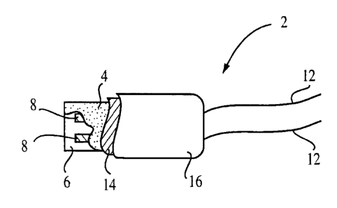
Figure 10 shows a cut-away view of an implantable analyte sensor;
Figure 11 shows an exploded view of an implantable analyte sensor; and
Figure 12 shows a cut-away view of an implantable analyte sensor.
DETAILED DESCRIPTION
Figure 10 shows a cut away view of an embodiment of the present invention. In
the
figure, an implantable analWe sensor 2 includes a substrate 6 on which are
electrodes 8
and 8. The electrode, are cowered with a membrane 4. Leads 12 and 12 allow for
elec-
trically connecting the implantable analyte sensor to external circuitry (not
shown). The
implantable analyte sensor also includes an external coating 16 and an
internal coating
14.
Figure 11 shows an exploded view of an embodiment of the present invention.
The
internal and external coatings are not included in the figure for clarity. As
shown in the
figure, the implantable analyte sensor 2 includes the electrodes 8 and 8 on
the substrate
6 surface, which are electrically connected with microelectronic circuitry 10.
The micro-
electronic circuitry is electrically connected to leads 12 and 12, which allow
for electri-
tally connecting the implantable analyte sensor to external circuitry (not
shown). The
electrodes are covered with the membrane 4.
Figure 12 shows a cut away view of an embodiment of the present invention
similar to
that shown in Figure 10, except for the presence of a third electrode 8 and a
third lead
CA 02406878 2002-09-13
WO 01/68901 PCT/EPO1/03027
4
12. Although so illustrated, the number of electrodes may be different from
the number
of leads.
The membrane is composed of a hard material that has been micromachined.
Prefera-
bly, the membrane comprises elemental silicon, but other hard, biocompatable
materials
that can be micromachined are possible, such as metals (for example titanium),
ceram-
ics (for example, silica or silicon nitride), and polymers (such as
polytetrafluoroethylene,
polymethylmethacrylate, polystyrenes and silicones). Micromachining is a
process that
includes photolithography, such as that used in the semiconductor industry, to
remove
material from, or add material too, a substrate. These techniques are well
known, and
are described, in Encyclopedia of Chemical Technology, Kirk-Othmer, Volume 14,
pp.
677-709 ( 1995); Semiconductor Device Fundamentals, Robert F. Pierret, Addison-
~~~esley, 1996; and Mlicrochip Fabrication 3rd. edition, Peter Van Zant,
McGraw-Hill,
1997. A detailed fabrication method for a membrane comprising elemental
silicon is
described in the dissertation of Derek James Hansford, submitted in partial
satisfaction
of the requirements for the degree of Doctor of Philosophy in Engineering-
Materials
Science and hfineral Engineering in the Graduate Division of the University of
Califor-
nia, Berkeley, submitted in the spring of 1999.
A special property of the membrane is a defined pore size, which has a small
size distri-
bution compared to the size distribution of standard membranes. Due to tight
toler-
ances in the manufacturing process, the pore size can be controlled at precise
diameters,
for example 1 to 50 nm, or ~ to 20 nm, or even 5 to 15 nm (such as 12 nm, 18
nm or
even 25 nm), with a variation of +/- 0.01-20%, +/-0.1-10% or even +/-1-5%.
Therefore
molecules above this size can be excluded with high certainty, since the size
distribution
has the shape of a top hat, rather than a bell curve, and hence pore sizes
above, for
example 12 nm, 18 nm, 25 nm or 50 nm are not present. These membranes can
exclude
interfering molecules, such as proteins, which could otherwise cause major
drift prob-
lems of the sensor, when the sensor is implanted in vivo. Signal drift is a
change in the
magnitude of the signal from a sensor which is unrelated to changes in analyte
concen-
tration. The amount of signal drift is based on the magnitude of the signal
prior to the
drifting. Preferably, the implantable analyte sensors of the present invention
exhibit a
signal drift of less than 20% per day in vivo, more preferably less than 10%
per day in
vivo, most preferably less than 5% per day in vivo.
CA 02406878 2002-09-13
WO 01/68901 PCT/EPO1/03027
Membranes for use in the present invention may be characterized by a glucose
diffusion
test and an albumin diffusion test. These tests are described below.
Preferably, the
membrane has a glucose diffusion test result of at least 1 mg/dl in 330 min.,
more pref
erably at least 10 mg/dl in 330 min., even more preferably at least 30 mg/dl
in 330 min.,
5 and most preferably at least 60 mg/dl in 330 min. Preferably, the membrane
has an
albumin diffusion test result of at most 0.1 g/dl in 420 min., more preferably
at most
0.05 g/dl in 420 min., even more preferably at most 0.01 g/dl in 420 min., and
most pref
erably at most 0.001 g/dl in 420 min.
The manufacturing process of the membranes may allow a simple and economical
pro-
duction of small, implantable analyte sensors. For example, the membranes can
be first
manufactured, and then on a substrate, the electrodes for the sensor and the
electrical
connectors can be formed. Preferably, the substrate is silicon, but other
materials are
possible, such as ceramics, or polymers. If desired, electronic components,
for example,
amplifiers, filters, transmitters and/or signal preconditioning components,
can easily be
incorporated in this layer. In particular, if the substrate comprises
elemental silicon, well
known integrated circuit technology may be used to place all the circuitry in
miniaturized form on a single chip.
There are two possible approaches to attach the substrate and the membrane,
when a
reagent is included in the sensor:
1. The substrate and the membrane are thermally bonded before the reagent is
depos-
ited on the electrodes. In this case, an opening, preferably in the membrane
is pro-
vided (since this may be manufactured with a micromachining process, an
opening
is easily generated during one of the processing steps). In the case where
multiple
membranes are formed as a single piece, and or multiple substrates are formed
as a
single piece, after thermal bonding, a further etching step may be used to
separate
the individual membrane/substrate units. The reagent is deposited through the
in-
dividual openings and the openings are sealed using, for example a polymer
sealant.
The individual sensors are then separated, incorporated into a flexible, inner
coat-
ing, for example silicone rubber, and individually coated with an outer
coating,
such as a biocompatible layer.
2. The reagent is deposited on the electrodes before the membrane and
substrate are
attached. In this case, thermal bonding is not possible, since the enzyme in
the rea-
gent would be destroyed. The individual membranes and substrates are first
sepa-
CA 02406878 2002-09-13
WO 01/68901 PCT/EPO1/03027
6
rated and the individual sensors are assembled by bonding one membrane with
one
substrate using a suitable bonding agent, for example, cyanoacrylate. As a
final step,
the individual sensors are incorporated into a flexible, inner coating, for
example
silicone rubber, and individually coated with an outer coating, such as a
biocom-
patible layer. The sensor can be inserted into the skin using a needle
applicator. The
control unit typically remains outside the body and can be connected to the
sensor
element through electrical wires (leads).
The electrodes are formed on the surface of the substrate. They may be formed
by well
known semiconductor processing techniques, from conductive materials, such as
pure
metals or alloys, or other materials which are metallic conductors. Examples
include
aluminum, carbon (such as graphite), cobalt, copper, gallium, gold, indium,
iridium,
iron, lead, magnesium, mercury (as an amalgam), nickel, niobium, osmium,
palladium,
platinum, rhenium, rhodium, selenium, silicon (such as highly doped
polycrystalline
silicon), silver, tantalum, tin, titanium, tungsten, uranium, vanadium, zinc,
zirconium,
mixtures thereof, and alloys or metallic compounds of these elements.
Preferably, the
electrodes include gold, platinum, palladium, iridium, or alloys of these
metals, since
such noble metals and their alloys are unreactive in biological systems. The
electrodes
may be any thickness, but preferably are 10 nm to 1 mm, more preferably, 20 nm
to
100 ~tm, or even 25 nm to 1 ym.
At least two electrodes must be present. The number of electrodes may be 2-
1000, or 3-
200, or even 3-99. Individual electrode sets (2 or 3 electrodes) may be
separated into
individual chambers, each covered with the membrane. Furthermore, individual
elec-
trode sets (2 or 3 electrodes] may each have a different reagent, allowing for
an im-
plantable analyte sensor that can measure at least two, such as 3-100, or 4-
20, different
analytes.
The remaining individual part of the implantable analyte sensors are well
known to
those of ordinary skill in the art, and are described, for example, in U.S.
Patent numbers
5,387,327; 5,411,647; and 5,476,776; as well as in PCT International
Publication num-
bers WO 91/15993; VVO 94/20602; VVO 96/06947; and WO 97/19344.
Although illustrated with both leads and microelectronic circuitry, these
components
are optional. The microelectronic circuitry may include some or all of the
electrical
components normally external to the implantable analyte sensor, such as a
microproc-
CA 02406878 2002-09-13
WO 01/68901 PCT/EPO1/03027
7
essor, an amplifier, or a power supply. If the microelectronic circuitry also
includes a
transmitter, or another device for sending information wirelessly, such as a
laser which
emits light through the skin, then there is no need to include the leads.
Alternatively, the
microelectronic circuitry may not be present, in which case the lead will
directly
electrically connect the electrodes with external electrical components.
Optionally, one or more internal coatings may be present. The internal coating
may
function to regulate diffusion. Examples of internal coatings include
cellulose acetate,
polyurethanes, polyallylamines (PAL), polyaziridine (PAZ), and silicon-
containing
polymers. Some specific examples are described in PCT Publications WO
98/17995, WO
98/13685 and WO 96/06947, and in U.S. Patent Nos. 4,650,547 and 5,165,407.
Optionally, one or more external coatings may be present. The implantable
analyte
sensors of the present invention are intended to be used in vivo, preferably
subcutane-
ously in mammals, such as humans, dogs or mice. The external coatings function
to
improve the biocompatibility of the implantable analyte sensor. Examples of
external
coatings include nafion, polyurethanes, polytetrafluoroethylenes (PTFE), poly
(ethylene
oxide) (PEO), and 2-methacryloyloxyethyl phosphorylcholine-co-n-butyl
methacrylate
(MPC) membranes. Some specific examples are described in PCT Publication
WO 96/06947, and in "Medical Progress through Technology", Nishida et al. 21:
91-103
(1995).
The electrodes may be coated with a reagent. The reagent is optional, and may
be used
to provide electrochemical probes for specific analytes. The reagent may be as
simple as
a single enzyme, such as glucose oxidase or glucose hydrogenase for the
detection of glu-
cose. The enzyme may be immobilized or "wired" as described in PCT Publication
WO
96/06947. The reagents may optionally also include a mediator, to enhance
sensitivity of
the sensor. The starting reagents are the reactants or components of the
reagent, and are
often compounded together in liquid form before application to the electrodes.
The
liquid may then evaporate, leaving the reagent in solid form. The choice of
specific rea-
gent depends on the specific analyte or analytes to be measured, and are well
known to
those of ordinary skill in the art. For example, a reagent for measurement of
glucose can
contain 62.2 mg polyethylene oxide (mean molecular weight of 100-900
kilodaltons), 3.3
mg NATROSOL 250 M, 41.5 mg AVICEL RC-591 F, 89.4 mg monobasic potassium
phosphate, 157.9 mg dibasic potassium phosphate, 437.3 mg potassium
ferricyanide,
46.0 mg sodium succinate, 148.0 mg trehalose, 2.6 mg TRITON X-100 surfactant,
and
CA 02406878 2002-09-13
WO 01/68901 PCT/EPO1/03027
2,000 to 9,000 units of enzyme activity per gram of reagent. The enzyme is
prepared as
an enzyme solution from 12.5 mg coenzyme PQQ and 1.21 million units of the
apoen-
zyme of quinoprotein glucose dehydrogenase, forming a solution of quinoprotein
glu-
cose dehydrogenase. This reagent is described in WO 99/30152, pages 7-10,
hereby in-
corporated by referece.
Other non-limiting examples of enzymes and optional mediators that may be used
in
measuring particular analytes in the present invention are listed below in
Table 1.
TABLE 1
Analyte Enzymes Mediator Additional Mediator
(Oxidized
Form)
Glucose Glucose Dehydro-Ferricyanide
genase and Diapho-
rase
Glucose Glucose-Dehydroge-Ferricyanide
vase
Cholesterol (Quinoprotein) Ferricyanide2,6-Dimethyl-1,4-
Cholesterol Benzoquinone
Esterase
and Cholesterol 2,5-Dichloro-1,4-
Oxidase Benzoquinone
or
Phenazine Ethosulfate
HDL CholesterolCholesterol Ferricyanide2,6-Dimethyl-1,4-
Esterase
and Cholesterol Benzoquinone
Oxidase 2,5-Diehloro-1,4-
Benzoquinone
or
Phenazine Ethosulfate
TriglyceridesLipoprotein FerricyanidePhenazine Methosul-
Lipase, or
C~lycerol Kinase,Phenazine fate
and
Glycerol-3-Phos-Ethosulfate
phate Oxidase
Lactate Lactate OxidaseFerricyanide2,6-Dichloro-1,4-
Benzoquinone
Lactate Lactate Dehydroge-Ferricyanide
nase and DiaphorasePhenazine
Ethosulfate,
or
Phenazine
Methosulfate
Lactate Diaphorase FerricyanidePhenazine Ethosul-
Dehydrogenase fate, or Phenazine
Methosulfate
uvate
Alco
amore
Bilirubin Bilirubin Oxidase 1-Methoxv-
Phenazine
Methosulfate
Uric Acid Uricase Ferricyanide
CA 02406878 2002-09-13
WO 01/68901 PCT/EPO1/03027
9
In some of the examples shown in Table 1, at least one additional enzyme is
used as a
reaction catalyst. Also, some of the examples shown in Table 1 may utilize an
additional
mediator, which facilitates electron transfer to the oxidized form of the
mediator. The
additional mediator may be provided to the reagent in lesser amount than the
oxidized
form of the mediator. While the above assays are described, it is appreciated
that a vari-
ety of electrochemical assays may be conducted in accordance with this
disclosure.
Formation of membrane
The following describes how to make a membrane for use in the present
invention,
based on the description from the dissertation of Derek James Hansford,
submitted in
partial satisfaction of the requirements for the degree of Doctor of
Philosophy in Engi-
neering-Materials Science and Mineral Engineering in the Graduate Division of
the
University of California, Berkeley, submitted in the spring of 1999.
Other membranes, made from other material, may also be used. This specific
method
relies upon a buried nitride etch stop layer.
The buried nitride etch stop layer acts as an etchant stop during the
formation of nano-
meter scale pores. The buried nitride etch stop layer facilitates three-
dimensional control
of the pore structure, and facilitates the formation of pores less than 50
nanometers in
diameter. Moreover, these pores can be uniformly formed across the entire
wafer.
Preferably, the first step in the fabrication protocol is to etch a support
ridge structure
into a substrate. The ridges provide mechanical rigidity to the subsequently
formed
membrane structure.
A low stress silicon nitride (LSN or nitride), which operates as an etch stop
layer, is then
deposited on the substrate using low pressure chemical vapor depositions
(LPCVD). In
one embodiment, 0.4 ~m of nitride was used. The resultant structure is shown
in
Figure 1. Figure 1 illustrates a substrate 20 with a nitride etch stop layer
22 formed
thereon.
The base structural layer (base layer) of the membrane is deposited on top of
the stop
layer 22. Since the etch stop layer 22 is thin, the structural layer is
deposited down into
the support ridges formed in the substrate 20. In one embodiment, 5 ~m of
polysilicon
is used as the base layer. Figure 2 illustrates the base layer 24 positioned
on the etch stop
CA 02406878 2002-09-13
WO 01/68901 PCT/EPO1/03027
layer 22. Low stress silicon nitride may also be used as the base layer, in
which case it
operates as its own etch stop layer.
The next processing step is to etch holes in the base layer 24 to define the
shape of the
pores. Masks, such as those used in traditional semiconductor processing, may
be used
5 to define the pores. For example, the holes may be etched through the
polysilicon by
chlorine plasma, with a thermally grown oxide layer used as a mask. In this
step, it is
important to make sure the etching goes completely through the base layer 24,
so a 10-
15% overetch is preferably used. It is useful to note that the buried nitride
etch stop 22
acts as an etch stop for the plasma etching of a silicon base layer 24.
Otherwise, if the
10 plasma punched through the nitride, tighter control of the etch step would
have to be
exercised to prevent the complete removal of the nitride under the plug layer
(to prevent
removal in the final 1~OH etch). Figure 3 illustrates the result of this
processing. In
particular, the figure illustrates holes 26 formed in the base layer 24, but
terminating in
the nitride etch stop layer 22.
Pore sacrificial oxide is subsequently grown on the base layer 24. Figure 4
illustrates a
sacrificial oxide 28 positioned on the base layer 24.
The sacrificial oxide thickness determines the pore size in the final
membrane, so con-
trol of this step is critical to reproducible membranes. This is accomplished
by the
thermal oxidation of the base layer 24 (e.g., a growth temperature of between
850-950°C
for approximately one hour with a ten minute anneal). Naturally, many
techniques may
be used to form a controlled thickness sacrificial layer. For example, a
thermally evapo-
rated tungsten film may be used as a sacrificial layer for polymer membranes
and selec-
tively removed with hydrogen peroxide. The basic requirement of the
sacrificial layer is
the ability to control the thickness with high precision across the entire
wafer. Thermal
oxidation of both polysilicon and nitride allows the control of the
sacrificial layer thick-
ness of less than 5% across the entire wafer. Limitations on this control
arise from local
inhomogeneities in the base layer, such as the initial thickness of the native
oxide (espe-
cially for polysilicon) the grain size or the density, and the impurity
concentrations.
To mechanically connect the base layer 24 with the plug layer (necessary to
maintain the
pore spacing between layers), anchor points were defined in the sacrificial
oxide layer 26.
In the present design, this is accomplished by using the same mask shifted
from the pore
holes by 1 ~tm diagonally. This produced anchors in one or two corners of each
pore
CA 02406878 2002-09-13
WO 01/68901 PCT/EPO1/03027
11
hole, which provides the desired mechanical connection between the structural
layers
while opening the pore area as much as possible. Figure 5 illustrates anchors
30 formed
via this process.
A plug structural layer is subsequently deposited to fill in the holes 26.
This step has
been implemented by depositing 1.5 ~m of polysilicon. The resultant plug layer
32 is
shown in Figure 6.
To open the pores at the surface, the plug layer 32 is planarized down to the
base layer,
leaving the final structure with the plug layer only in the pore hole
openings, as shown in
Figure 7.
The method of planariration depends on the material used as the plug material.
For the
hard micro-fabrication materials (polysilicon and nitride), chemical
mechanical polish-
ing was used for planarization. The other materials studied were roughly
planarized
using a plasma etch, with a quick wet chemical smoothing. This technique has
the
advantage that, assuming it is not etched by the plasma used, the base layer
is not
affected, but has the disadvantage of the need for controlled etch timing to
avoid com-
pletely etching the plugs themselves.
At this point, the membrane is ready for release, so a protective layer 34 is
deposited on
the wafer (completely covering both sides of the wafer). The requirements of
the pro-
tective layer 34 are that it be impervious to the silicon etch (KOH for these
studies) and
that it be removed without removing the plug 32 or base 24 structural layers.
For poly-
silicon and nitride structural layers, a thin nitride layer is used as the
protective layer
(nitride is not etched at all by KOH and dissolves slowly in HF). For
polymeric struc-
tural materials, silicon is used as a protective layer, due to the processing
temperature
necessary for nitride deposition (835° C).
The backside etch windows were etched in the protective layer, exposing the
silicon in
desired areas, and then the entire structure was placed in an 80°C KOH
bath until the
silicon wafer substrate 20 is etched up to the membrane base layer 24 (as
evidenced by
the smooth buried etch stop layer). Figure 8 illustrates the resultant
aperture 36 formed
in the substrate 20.
CA 02406878 2002-09-13
WO 01/68901 PCT/EPO1/03027
12
At this point, the buried nitride layer 22, the sacrificial oxide layer 34,
and plug layer 32
are removed by etching in HF or SF6/oxygen plasma. The resultant membrane 4
with
nanometer scale pores is shown in Figure 9.
Characterization of membranes
The purpose of the membranes is to allow the analyte of interest (such as
glucose) to
diffuse through the membrane, while excluding large molecules (such as
proteins).
Therefore, two important characteristics of the membranes are glucose
diffusion and
albumin diffusion. All tests are carried out at room temperature
(25°C).
The following is a glucose diffusion test:
Diffusion of glucose is measured using a mini diffusion chamber constructed
around the
membranes. The diffusion chamber, fabricated out of acrylic, consists of two
compart-
ments A and B with fixed volumes of 2 ml, separated by the desired membrane,
sealed
with o-rings, and screwed together.
Glucose is measured on either side of the membrane using the diffusion chamber
by
means of a quantitative enzymatic assay (TRINDERT~~, SIGMA) and colorometric
reading via a spectrophotometer. Starting glucose concentrations for all tests
were 6,666
mg/dl and 0.0 mg/dl in chambers A and B, respectively. Samples of 0.1 ml are
taken
from the diffusion chamber and 10 ftl of that are added to 3 ml of glucose
reagent in a
cuvette, and mixed gently by inversion. Each tube is incubated for 18 minutes
at room
temperature and then readings are taken at a wavelength of 505 nm. The reagent
is
linear up to 750 mg/dl. The diffusion chamber itself is attached to a motor
for stirring in
order to minimize boundary layer effects (diffusion resistance at the
liquid/membrane
interface). In order to ensure wetting of the pores, the receptor cell is
first filled with
phosphate buffer saline (PBS) for fifteen minutes before the filling of the
donor cell. The
donor cell is filled with solutions of glucose in PBS in varying
concentrations.
The following is an albumin diffusion test:
Albumin is also measured on either side of the membrane using the same
diffusion
chamber as in the glucose diffusion test. Albumin diffusion and/or exclusion
is first
measured and quantified using Albumin BCP (bromocresol purple, SIGMA).
Starting
albumin concentrations for all tests are 4 g/dl and 0.0 mg/dI in chambers A
and B,
CA 02406878 2002-09-13
WO 01/68901 PCT/EPO1/03027
13
respectively. A sample of 0.1 ml is taken at time zero and at the end of the
diffusion
period (time = 330 minutes). An aliquot of 300 ~l is then added to 3 ml of the
reagent
and absorbence is read at 600 nm. Reagent plus deionized water is used as the
blank. The
BCP assay is linear up to 6g/dl but is not accurate below 1 g/dl. For the
small con-
centration of albumin that might be present in chamber A, the presence of any
protein
in chamber B is measured using the Bradford Method (MICRO PROTEIN KIT,
SIGMA). This method quantitates the binding of Coomassie brilliant blue to an
unknown protein and compares this binding to that of different amounts of a
standard
protein. Albumin is used as a standard protein. This method quantifies 1 to
100 micro-
grams protein using a standard curve, with sensitivity down to 10 mg/dl or 0.1
g/dl pro-
tein. The absorbance is measured at 595 nm.
Analysis of membranes
Diffusion of glucose was measured for three types of membranes: silicon
micromachi-
ned membranes (average pore size = 0.0245 microns), WHATMAN ANODISC mem-
branes (average pore size = .02 microns), and MF-MILLIPORE mixed cellulose
acetate
and nitrate membrane (average pore size = 0.025 microns).
The results from the albumin test are shown in the table below.
WHATMAN MILLIPORE silicon
(micromachined)
time albumin conc. albumin conc. albumin conc.
(g/dL) (g/dL) (g/dL)
0 0 0 0
420 MinØ25'c'0.05 0.2b'0.01 0b'0.001
The presence of albumin does not seem to impede passage of glucose through the
mem-
branes, nor slow down glucose transport. No detectable amounts of albumin
diffuse
through the micromachined membrane. The same membrane, however, shows glucose
diffusion. The micromachined membranes are able to achieve complete exclusion
of
albumin (to within the limits of detection), while allowing glucose diffusion.
Comparing
diffusion rates with that of commercially available membranes, the
micromachined
membranes have glucose diffusion properties comparable to MIILLIPORE and
alumina
WHATMAN membranes with similar pore sizes.
CA 02406878 2002-09-13
WO 01/68901 PCT/EPO1/03027
14
The passage of albumin through the micromachined membrane is measured by
looking
at the change of albumin concentration in chamber A and chamber B over time.
Using
the BCP assay, there are no detectable traces of albumin in chamber B.
However, the
amount of albumin in chamber B may have been below the limits of detectability
of this
assay system. Therefore, the Bradford Method was also employed. Using this
microas-
say, again no detectable amounts of albumin were found in chamber B for the
micro-
machined membrane, but small amounts of protein were found in chamber B using
both the MILLIPORE and WHATMAN membranes. The amounts of albumin detected
after 420 minutes in chamber B were approximately 0.25 g/dI and 0.20 g/dI
albumin for
the MILLIPORE and WHATh-lAN membranes, respectively.
Glucose does diffuse through micromachined membranes at a rate comparable to
com-
mercially available membranes. At the same time, albumin is excluded from
passage. In
mixed solutions of glucose and albumin, only glucose diffuses through the
micromachi-
ned membranes.