Note: Descriptions are shown in the official language in which they were submitted.
CA 02406956 2002-10-18
WO 02/073250 PCT/EP02/01586
-1-
Magnetic thin film interference device or pigment and method of
making it, printing ink or coating composition, security docu-
ment and use of such a magnetic thin film interference device
Field of invention
The present invention is in the field of optically variable pig-
ments. In particular, it describes a magnetic thin film inter-
ference device, a method of making such a magnetic thin film in-
terference device, a magnetic thin film interference pigment, a
printing ink or coating composition, a security document and the
use of such a magnetic thin film interference device, all ac-
cording to the definition of the patent claims.
Background of the invention
Optically variable devices of various types are used as an effi-
cient anti-copy means on bank notes and security documents. A
large part of the world-wide printed currency relies on such op-
tically variable copy protection devices, and among these, fea-
tures printed with optically variable ink (OVI'') have acquired a
preeminent position since their first appearance on currency in
1987.
Optically variable pigment (OVP) shows a viewing-angle dependent
color appearance which cannot be reproduced by color copying
equipment. Various different types of OVP materials are commer-
cially available today.
CA 02406956 2002-10-18
WO 02/073250 PCT/EP02/01586
-2-
Very brilliant colors are obtained with a first type of OVP,
made by physical vapor deposition. This type of OVP is con-
structed as a thin-film vapor-deposited Fabry-Perot resonator
stack. Simple-sandwich metal-dielectric-metal, as well as dou-
ble-sandwich metal-dielectric-metal-dielectric-metal layer se-
quences are described in the prior art. The top metal layer(s)
must be partially reflecting / partially transparent, such that
light can be coupled in and out of the Fabry-Perot resonator
stack.
Said optically variable thin-film material is obtained as a con-
tinuous sheet on a carrier foil. It can subsequently be detached
from its carrier and comminuted into a pigment, which consists
of flakes having a diameter of 20 to 30 gm and a thickness of
about 1 m. This pigment can be formulated into inks or coating
compositions, preferably for screen-printing or intaglio-
printing applications.
The optical variability of said pigments relies on an interfer-
ence effect. Incident light falling upon an OVP flake of said
metal-dielectric-metal type is partially reflected at the top
metal layer and partially transmitted, travelling through the
dielectric layer and reflected back at the bottom metal layer.
Both reflected parts of the incident light finally recombine and
interfere with each other. Constructive or destructive interfer-
ence results, depending on the thickness of'the dielectric layer
and on the wavelength of the incident light. in the case of
white incident light, some of the white light components, having
determined wavelengths, are reflected, whereas other components,
having other wavelengths, are not reflected. This gives rise to
a spectral selection, and hence to the appearance of color.
CA 02406956 2002-10-18
WO 02/073250 PCT/EP02/01586
-3-
The path difference between the top-reflected and the bottom-
reflected part of the light depends noteworthy on the angle of
incidence, and so does the resulting interference color.
Another, second type of OVP, is based on coated aluminum flakes.
Mechanically flattened aluminum particles are coated by chemical
vapor deposition (CVD) or by wet chemical methods with a dielec-
tric layer and a subsequent metal or second dielectric layer.
Interference colors result by the same effect as described
above. This type of OVP is cheaper in manufacture than the first
type, but it also exhibits less brilliant colors and less angle-
dependent color shift than the first type.
Large amounts of "optically variable" and "iridescent" pigment
are produced for merely decorative purposes (automotive paints,
lacquers, toys and the like), and are thus available to the com-
mon public in the form of coating compositions. The security po-
tential of optically variable ink features on bank notes is con-
siderably decreased if no clear distinction can be established
between "Security OVP" and "Decorative OVP". A counterfeiter
could noteworthy reproduce bank notes on a color copier and add
the missing optically variable features with the help of a com-
mercially available decorative paint or spray.
For these and other reasons, security OVP must be made materi-
ally distinguishable from the merely decorative, commercially
available types of"OVP. An effective way of doing this is to
dope the security OVP with a covert magnetic feature. The "mag-
netic OVP" allows noteworthy the implementation of different
levels of security into correspondingly marked documents: i) a
simple "magnetic present/not present" feature; ii) identifica-
tion of the magnetic characteristics of the feature; iii) a
printed pattern of magnetic and non-magnetic features; and iv) a
CA 02406956 2002-10-18
WO 02/073250 PCT/EP02/01586
-4-
magnetic data carrier, allowing magnetic storage of information
in the printed magnetic OVP feature.
Such magnetic OVP has been proposed in US 4,838,648. A particu-
lar magnetic material is, to this purpose, incorporated into the
OVP design. The OVP of US 4,838,648 is of the metal(reflector)-
dielectric-metal(absorber) multilayer Fabry-Perot type, and has
preferably a magnetic cobalt-nickel 80:20 alloy as the reflector
layer. Alternatively, but less preferably, the magnetic alloy
may also be present as the absorber layer. The device according
to US 4,838,648 has noteworthy the shortcomings of i) showing a
degraded optical performance, in particular a lower chromatic-
ity, due to the lower reflectivity of cobalt-nickel alloy, as
compared to aluminum, and ii) the lack of freedom for choosing
the magnetic material. This latter must noteworthy comply at the
same time with the functions of a magnet and of a good optical
reflector, and there are only very few materials satisfying both
conditions.
It is a first goal of the present invention to provide security
OVP which is made materially different from decorative OVP
through the incorporation of particular magnetic properties.
It is another goal of the present invention to incorporate said
magnetic properties into said OVP without degrading the OVP's
chromaticity and color shifting properties.-
It is a further goal of the present invention to provide said
magnetic OVP with as large as possible freedom for selecting the
magnetic material.
It is still another goal of the present invention to provide se-
curity OVP which can be manufactured using the same equipment
CA 02406956 2002-10-18
WO 02/073250 PCT/EP02/01586
-5-
and process that are used for the production of "common", non-
magnetic OVP, without significantly increasing the production
cost.
Summary of the invention
The present invention refers to a magnetic thin film interfer-
ence device, made of OVP showing a viewing-angle dependent
color-appearance. The OVP is made of a multi-layer stack includ-
ing at least one light-reflecting reflector layer, at least one
light-transmitting dielectric layer, at least one light-
absorbing absorber layer and at least one magnetic layer. The
magnetic layer is separated from a dielectric layer by a reflec-
tor layer.
According to a first preferred embodiment of a magnetic OVP, the
magnetic layer is disposed within two reflector layers. The mag-
netic layer is symmetrically confined within two reflector lay-
ers, resulting in equal optical properties of the magnetic OVP
along two reflector layer sides.
According to a second preferred embodiment of a magnetic OVP,
the magnetic layer is adjacent to only one reflector layer, re-
sulting in an asymmetrically magnetic OVP with optical proper-
ties along solely one reflector layer side.
The magnetic OVP according to the present invention has the par-
ticular advantage that it is possible, by using the disclosed
layer sequence, to exactly match the color and the angular color
shift of a corresponding non-magnetic OVP, and at the same time
to provide an OVP with a wide variety of magnetic properties.
CA 02406956 2002-10-18
WO 02/073250 PCT/EP02/01586
-6-
The magnetic thin film interference device may be comminuted to
obtain a magnetic thin film interference pigment. Said magnetic
thin film interference pigment may be incorporated in a printing
ink or coating and/or on a security document.
The invention is further illustrated by drawings and examples:
Figure 1 shows a conventional OVP flake having a 5-layer design.
Figure 2 shows the cross section of a first preferred embodiment
of a magnetic OVP according to the invention, having
magnetic properties. A 7-layer design is employed.
Figure 3 shows the cross section of a second preferred embodi-
ment of a magnetic OVP according to the invention, hav-
ing magnetic properties. A 4-layer design is employed.
Figure 1 shows a cross section of an OVP of the first type de-
scribed above having a 5-layer design. Such pigment consists of
flakes, which are of the order of 20 to 30 pm large, and about 1
gm thick. Said flake has a symmetric "absorber / dielectric /
reflector / dielectric / absorber" layer structure, in order to
provide for equal optical properties on both sides. The absorber
layers 1, 1' are preferably thin (e.g. in the order of 3 to 5
nm) chromium or similar corrosion-resistant metal layers, which
act as beam-splitters, reflecting and transmitting parts of the
incident light. The dielectric layers 2, 2' are preferably of a
low dielectric constant material, such as magnesium fluoride
(MgF2; n = 1.38) or silicon dioxide, to enable a high angle-
dependent color shift. The thickness of the dielectric layers 2,
21 determines the OVP's color and is of the order of 200 to 800
nm (e.g. gold-to-green: 440 nm MgF2, green-to-blue: 385 nm MgF2).
A central, total light-reflecting reflector layer 3 is prefera-
CA 02406956 2002-10-18
WO 02/073250 PCT/EP02/01586
-7-
bly of aluminum, or of any other highly reflecting metal or
metal alloy, and has a thickness in the order of 10 to 100 nm.
Figure 2 shows the schematic layer sequence of a first preferred
embodiment of a magnetic OVP according to the present invention.
Said magnetic OVP comprises, two absorber layers 1, 1', two di-
electric layers 2, 2', and two reflector layers 3, 3'. At least
one magnetic layer 4 of magnetic material is disposed within
said reflector layers 3, 3', resulting in a symmetric "absorber
/ dielectric / reflector / magnetic / reflector / dielectric /
absorber" of a 7-layer design.
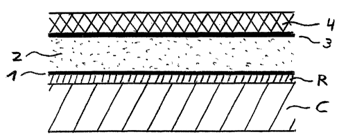
Figure 3, shows the schematic layer sequence of a second pre-
ferred embodiment of a magnetic OVP according to the present in-
vention. Said magnetic OVP comprises one absorber layer 1, one
dielectric layer 2 and at least one magnetic layer 4 being adja-
cent to one reflector layer 4. In this embodiment, a 4-layer de-
sign is required. Preferably, on a release-coated R carrier foil
C, an absorber layer 1 of chromium is deposited, followed by a
dielectric layer 2 of magnesium fluoride and a reflector layer 3
of aluminum. A magnetic layer 4 of magnetic material is depos-
ited at last. The device is subsequently applied to a substrate
with the magnetic layer facing the substrate, by e.g. using an
appropriate glue.
The magnetic layer 4 can be of any type of magnetic material,
e.g. iron, cobalt, nickel; magnetic alloys such as Ni-Co or Nd-
Fe-B; inorganic oxide compounds such as Fe203, Fe304, chromium di-
oxide Cr02, ferrites MFe2O4 (with M an ion or a cocktail of ions
selected from the group consisting of Mgt+, Cat+, Sr", Bat+, Mn2+,
Cot+, Fe2+, Nit+, Cut+, Zn2+, etc.), garnets A3B5012 (with A = a tri-
valent rare earth-ion or a cocktail of trivalent rare-earth ions
and B an ion or a cocktail of ions selected from the group con-
CA 02406956 2002-10-18
WO 02/073250 PCT/EP02/01586
-8-
sisting of Al", Cr3+, Fe3+, Ga3+, Bi3+, etc.) , hexaferrites MFe12019
with M selected from the group of divalent ions Ca2+, Sr2+, Bat+,
etc., perovskites, etc.
In the context of the present invention, any kind of not-
diamagnetic material may noteworthy be used to confer a particu-
lar magnetic property to the magnetic OVP. Said magnetic prop-
erty may for instance be: strong (super-) paramagnetism; ferro-
magnetism; ferrimagnetism; antiferromagnetism; antiferrimag-
netism; etc. The material may be of the soft-magnetic, low-
coercivity, medium-coercivity or hard-magnetic type, or it may
be laid out for detection by the Barkhausen effect. The magnetic
property may furthermore result in remanent magnetism comprised
in between zero Oersted up to as high as 10'000 Oersted.
The deposition of the magnetic material is performed by the same
method as used for the deposition of the dielectric layer or of
the metal layers of a nonmagnetic OVP of the first type men-
tioned above. MgF2, chromium or aluminum can noteworthy be depos-
ited by electron-beam assisted thermal evaporation. Magnetic al-
loys, such as cobalt-nickel or iron-cobalt-boron, are comparable
in melting point and evaporation characteristics with chromium,
and can therefore be deposited in a similar way, given the depo-
sition is performed at source temperatures above the material's
Curie or Neel temperature. For the deposition of oxide materi-
als, higher deposition temperatures are generally required, but
even these materials can be deposited by e-beam techniques. For
the deposition of more complex chemical compositions, ion-beam
assisted evaporation methods may be employed.
The magnetic layer 4 is covered by a reflector layer 3, 3' made
of a good light reflecting material, such as aluminum, aluminum.
alloy, chromium, silver, gold, etc. This allows the magnetic OVP
CA 02406956 2002-10-18
WO 02/073250 PCT/EP02/01586
-9-
to be optimized simultaneously for good optical performance as
well as for customer-designed magnetic properties. In this way,
different varieties of security-OVP can be produced, all having
exactly the same color appearance and color shifting properties,
but different magnetic properties. Using a corresponding mag-
netic detecting device, known to the skilled in the art, they
can easily be distinguished from each other, as well as from
non-magnetic OVP of the same optical appearance.
It is furthermore possible to use the primarily obtained opti-
cally variable and magnetic thin-film product directly as an op-
tically variable security foil, which may be applied to a docu-
ment or to an article, preferably by hot-stamping or cold-
stamping or related application methods.
A further property which can advantageously be exploited for se-
curity purposes is the particular form of the magnetization or
hysteresis curve of thin-film magnetic materials. Due to their
restricted third dimension, such materials often show a very
high squareness of their hysteresis curve, together with a vari-
able coercivity value which depends noteworthy on the layer
thickness and on the parameters used in the deposition of the
magnetic' layer. Such materials may also be laid out to show a
pronounced Barkhausen effect, which enables their detection by
techniques known from electronic article surveillance (EAS) ap-
plications. Alternatively, nonlinear magnetization effects may
.be exploited for detection, through the choice of the appropri-
ate magnetic materials, such as amorphous magnetic alloys or
magnetic garnets of low magnetic saturation. A wide field is
thus open for the engineering of OVP showing magnetic effects
and properties, which are very difficult to counterfeit on the
mere basis of mixing conventional OVP with conventional magnetic
materials.
CA 02406956 2002-10-18
WO 02/073250 PCT/EP02/01586
-10-
Said 7-layer magnetic OVP respectively 4-layer magnetic OVP can
noteworthy be manufactured using the same type of vacuum-
deposition equipment as is required for the manufacturing of the
conventional 5-layer non-magnetic OVP.
More than one layer of magnetic material may be present in the
magnetic OVP. In case of multiple layers of magnetic material,
said layers may be either of the same or of different magnetic
materials; said layers of magnetic material may furthermore be
either adjacent to each other or separated from each other by
layers of non-magnetic materials. Said magnetic layer 4 may be
multi-layer stacks, preferably layered superlattices. Layered
superlattices have been shown to display unusual electromagnetic
effects, such as Giant Magnetoresistance, non-linear high-
frequency response, unusual nuclear magnetic resonance signa-
tures, etc..
The magnetic OVP according to the invention may furthermore
carry additional overt or covert properties, such as indicia,
micro-texture, luminescence, radio-frequency or microwave reso-
nance absorption, etc..
Examples
In the first preferred embodiment of a magnetic OVP, depicted in
Figure 2, the magnetic layer 4 is comprised within two totally
reflector layers 3, 3' of the OVP stack. In order to provide for
optimal conditions of both, the optical and the magnetic func-
tion, the "standard" OVP layer sequence chromium / magnesium
fluoride / aluminum is used to implement the optical function.
The aluminum layer is "split in two", in order to accommodate
the magnetic functionality in its interior in the form of an ad-
CA 02406956 2002-10-18
WO 02/073250 PCT/EP02/01586
-11-
ditional layer of any desired magnetic element, alloy or com-
pound.
On a release-coated R carrier foil C, a first absorber layer 1
of chromium is deposited, followed by a first dielectric layer 2
of magnesium fluoride and a first reflector layer 3 of aluminum.
Then, the magnetic layer 4 of magnetic material is deposited,
followed by a second reflector layer 3' of aluminum. A second
dielectric layer 2' of magnesium fluoride and a second absorber
layer 1' of chromium are then deposited, to finish the magnetic
OVP multi-layer stack.
The skilled in the art will notice that any type of magnetic ma-
terial, amorphous or crystalline, such as a magnetic metal like
iron, cobalt, nickel, etc.; or a magnetic alloy, such as cobalt-
nickel, cobalt-chromium, terbium-iron, neodymium-iron-boron
etc.; or a magnetic refractory compound, such as a simple or a
complex oxide from the classes of ferrites, hexaferrites, gar-
nets, perovskites etc. can be used as the middle magnetic layer
between two aluminum reflector layers.
1. Soft magnetic green-to-blue OVP
in a first preferred embodiment of a magnetic OVP, soft magnetic
iron was used as the magnetic function carrier. A 7-layer se-
quence was deposited by electron beam assisted thermal evapora-
tion onto a release-coated R carrier foil C as follows:
1. Chromium metal, 3.5 nm thick (first absorber layer 1)
2. MgF2, 385 nm thick (first dielectric layer 2)
3. Aluminum metal, 40 nm thick (first reflector layer 3)
4. Iron metal, 200 nm thick (magnetic layer 4)
5. Aluminum metal, 40 nm thick (second reflector layer 3')
CA 02406956 2002-10-18
WO 02/073250 PCT/EP02/01586
-12-
6. MgF2, 385 nm thick (second dielectric layer 2')
7. Chromium metal, 3.5 nm thick (second absorber layer 1')
Total optical path at orthogonal incidence: 530 nm.
After the deposition being completed, the thin film product was
removed from the carrier foil C, comminuted to a pigment, and
used in inks and coating compositions.
In a variant of the first preferred embodiment of a magnetic
OVP, magnetic layer 4 was made of nickel metal, to yield a low-
coercivity optically variable pigment.
In a further variant of the first preferred embodiment of a mag-
netic OVP, magnetic layer 4 was made of cobalt metal, to yield a
medium-coercivity optically variable pigment, which is further-
more susceptible to detection by cobalt-59 nuclear magnetic
resonance in its own magnetic field, in the 214 MHz region.
In still a further variant of the first preferred embodiment of
a magnetic OvP, magnetic layer 4 was made of gadolinium metal,
to yield optically variable pigment which is ferromagnetic below
16 C, the Curie temperature of gadolinium metal.
2. Low-coercivity gold-to-green OVP
In another variant of the first preferred embodiment of a mag-
netic OVP, a low-coercivity, amorphous, Barkhausen-active EAS
material of the composition Fe50Co25Si10B15 was used as the mag-
netic function carrier. A 7-layer sequence was deposited by
electron-beam assisted thermal evaporation onto a release-coated
R carrier foil C as follows:
CA 02406956 2002-10-18
WO 02/073250 PCT/EP02/01586
-13
1. Chromium metal, 3.5 nm thick (first absorber layer 1)
2. MgF2, 440 nm thick (first dielectric layer 2)
3. Aluminum metal, 40 nm thick first reflector layer 3)
4. Fe50Co25Si10B15, 500 nm thick ( magnetic layer 4)
5. Aluminum metal, 40 nm thick (second reflector layer 3')
6. MgF2, 440 nm thick (second dielectric layer 2')
7. Chromium metal, 3.5 nm thick (second absorber layer 1')
Total optical path at orthogonal incidence: 605 nm.
The complex amorphous Fe50Co25Si10B15 alloy can also advantageously
be deposited by argon ion-beam assisted thermal evaporation.
After the deposition being completed, the thin film product was
removed from the carrier, comminuted to a pigment, and used in
inks and coating compositions.
This material shows a sharp Barkhausen discontinuity on magneti-
zation change in the magnetic field range below 1 Oersted.
3. Medium coercivity green-to-blue OVP
In another variant of the first preferred embodiment of a mag-
netic OVP, a medium-coercivity cobalt ferrite of the composition
CoFe2O4 was used as the magnetic function carrier. A 7-layer se-
quence was deposited by electron-beam assisted thermal evapora-
tion onto a release-coated (R) carrier foil (C) as follows:
1. Chromium metal, 3.5 nm thick (first absorber layer 1)
2. MgF2, 385 nm thick (first dielectric layer 2)
3. Aluminum'metal, 40 nm thick (first 'reflector layer 3)
4. CoFe2O4, 100 nm thick (magnetic layer 4)
5. Aluminum metal, 40 nm thick (second reflection layer 3')
6. MgF2, 385 nm thick (second dielectric layer 2')
CA 02406956 2002-10-18
WO 02/073250 PCT/EP02/01586
-14-
7. Chromium metal, 3.5 nm thick (second absorber layer 1')
Total optical path at orthogonal incidence: 530 nm.
The CoFe2O4 ferrite material can also advantageously be deposited
by argon ion-beam assisted thermal evaporation.
After the deposition being completed, the thin film product was
removed from the carrier, comminuted to a pigment, and used in
inks and coating compositions.
An optically variable patch containing magnetic OVP manufactured
according to this embodiment was successfully used as a track
for the magnetic storage of security information, such as the
hidden cross-checking information in transportation tickets,
bank cards, credit or access cards.
4. High coercivity green-to-blue OVP
In another variant of the first preferred embodiment of a mag-
netic OVP, a high-coercivity, barium ferrite material of the
composition BaFe12O19 was used as the magnetic function carrier. A
7-layer sequence was deposited by electron-beam assisted thermal
evaporation onto a release-coated R carrier foil C as follows:
1. Chromium metal, 3.5 nm thick (first absorber layer 1)
2. MgF2, 385 nm thick (first dielectric layer 2)
3. Aluminum metal, 40 nm thick (first reflector layer 3)
4. BaFe12O19, 300 nm thick (magnetic layer 4)
5. Aluminum metal, 40 nm thick (second reflector layer 3')
6. MgF2, 385 nm thick (second dielectric layer 2')
7. Chromium metal, 3.5 nm thick (second absorber layer 1')
Total optical path at orthogonal incidence: 530 nm.
CA 02406956 2002-10-18
WO 02/073250 PCT/EP02/01586
-15-
The BaFeJ12O19 ferrite material can also advantageously be depos-
ited by argon ion-beam assisted thermal evaporation.
After the deposition being completed, the thin film product was
removed from the carrier, comminuted to a pigment, and used in
inks and coating compositions.
An optically variable patch containing magnetic OVP manufactured
according to this variant of the preferred embodiment was suc-
cessfully used as a track for irreversibly written magnetic se-
curity information, e.g. hidden authenticating information in a
credit or access card. A special, not commonly available hard-
ware was required to magnetize the 3000 Oersted coercivity bar-
ium ferrite material, in order to write said security informa-
tion.
The OVP according to the foregoing embodiments can be incorpo-
rated into inks or coating compositions and applied to articles
by any printing or coating method, such as intaglio, silk screen
or transfer printing; alternatively they can be molded or lami-
nated into plastic material.
The present invention also discloses optically variable foils
having magnetic properties, which constructed according to the
same principles as said optically variable pigments. Such foils
noteworthy comprise an at least 4-layer stack, comprising an op-
tical part and at least one additional magnetic layer on top of
it.
More than one magnetic layer 4 of magnetic material may be pres-
ent in the optically variable foil. in case of multiple magnetic
layers 4, said layers may be adjacent to each other or separated
by layers of non-magnetic material. The magnetic layers 4 may
CA 02406956 2002-10-18
WO 02/073250 PCT/EP02/01586
- 16-
furthermore be either of the same, or of different magnetic ma-
terials. The optically variable foil according to the invention
may furthermore carry additional overt or covert properties,
such as,indicia, micro-texture, luminescence, radio-frequency or
microwave resonance, etc..
The magnetic layer side of the foil will be applied onto a sub-
strate, using an appropriate transfer technique, such as hot- or
cold-stamping, in conjunction with an appropriate glue.
5. Medium-coercivity gold-to-green OVP foil
In a second preferred embodiment of a magnetic OVP, a medium-
coercivity iron oxide is used as the magnetic function carrier
in an OVP foil. A 4-layer sequence was deposited by electron-
beam assisted thermal evaporation onto a release-coated R car-
rier foil C as follows:
1. Chromium metal, 3.5 nm thick (absorber layer 1)
2. MgF2, 440 nm thick (dielectric layer 2)
3. Aluminum metal, 40 nm thick (reflector layer 3)
4. Fe2031 500 nm thick (magnetic layer 4)
Total optical path at orthogonal incidence: 605 nm.
The Fe203 material can also advantageously be deposited by argon
ion-beam assisted thermal evaporation.
After the deposition being completed, the foil was coated with a
hot-melt glue composition and applied to security documents us-
ing a hot-stamping die of elongated form, to form an optically
variable magnetic track. Authentication information was then
magnetically written into said security track.
CA 02406956 2002-10-18
WO 02/073250 PCT/EP02/01586
-17-
6. Activatable-deactivatable EAS green-to-blue OVP foil
In a variant of the second preferred embodiment of a magnetic
OVP, a multilayer magnetic material was used as the magnetic
function carrier. The device consists of a Barkhausen-active EAS
layer of Fe6oCo15Si1oB15, followed by a low-coercivity nickel
layer. The following sequence was deposited by electron beam as-
sisted thermal evaporation onto a release-coated R carrier foil
C, as follows:
1. Chromium metal, 3.5 nm thick (absorber layer 1)
2. MgF2, 385 nm thick (dielectric layer 2)
3. Aluminum metal, 40 nm thick (reflector layer 3)
4. Fe60Co15Si1oB1s, 200 nm thick (first magnetic layer 4)
5. Nickel metal, 200 nm thick (second magnetic layer 4)
Total optical path at orthogonal incidence: 530 nm.
The Fe6oCo15Si1oB15 material can also advantageously be deposited
by argon ion-beam assisted thermal evaporation.
After the deposition being completed, the foil was applied to
security documents using a pre-printed, UV-activated glue patch
and a cold-stamping die in the form of optically variable mag-
netic security seals.
If the nickel layer is in a magnetized state, the Fe60Co3.5Si10B15
layer will not respond to the Barkhausen interrogating field,
which is an alternating magnetic field having a maximum field
strength below 5 Oersted. At the end of a demagnetization cycle,
however, the Barkhausen-active material can be detected through
its characteristic response. It is then protected again by a re-
magnetization of the nickel layer.