Note: Descriptions are shown in the official language in which they were submitted.
CA02407209 2002-10-23
-1-
STAMPING TOOL, METHOD FOR STRUCTURING A SURFACE OF A
WORKPIECE AND USE OF AN ANODIZED SURFACE LAYER
s The present invention relates to a stamping tool having a structured
stamping sur-
face, a method for producing a stamping tool having a structured stamping sur-
face, a method for structuring a surface of a work piece and use of a surface
layer
provided with open hollow chambers by anodic oxidation.
io Stamping constitutes a non-cutting manufacturing method for producing a
relief
like or structured surface on a work piece. A stamping tool with a profiled or
structured stamping surface is used for this. The stamping surface is pressed
with
such a stamping force onto the surface to be structured of the work piece or
rolled on this, so that the work piece becomes plastic and flows into
depressions
is in the stamping tool or the stamping surface. Due to the considerable
stamping
forces employed, the stamping tool and the stamping surface are usually made
of
metal.
It is very expensive to manufacture a stamping tool with a very finely
structured
20 or profiled stamping surface. To create a so-called "moth eye structure" -
evenly
arranged, egg carton-like bumps - or fine grooves in the nanometre range, it
is
known from practice to use a lighting pattern with periodic intensity
modulation
for illuminating photo-sensitive material via two interfering laser beams.
After
the illuminated material develops, a periodic surface structure results, which
is
2s moulded into other materials using various replication methods and finally
into
nickel, for example, by electroforming. This type of manufacturing is very ex-
pensive and is suited only for structuring even surfaces.
In the present invention nanometre range is understood to mean profiling or
3o structuring with structural widths < 1000 nm, especially < S00 nm. The
structural
width designates the dimension by which individual structural elements, such
as
bumps, are repeated, that is, for example the average distance of adjacent
bumps
from one another or of depressions from one another.
CA 02407209 2002-10-23
_ 2' - _.
In the nanometre range lithographic methods for structuring a stamping surface
of a stamping tool can still only be used in a limited way. It should be noted
here
that the wavelength of the visible light alone is already 400 to 750 nm. In
each
case lithographic methods are very costly.
s
DE 197 27 132 C2 discloses the manufacturing of a stamping tool by means of
electrolytic machining. During electrolytic machining a metallic stamping sur-
face of the stamping tool is treated electrolytically, wherein, being an anode
in a
fast-flowing electrolyte, the metal of the stamping surface is located at a
minimal
distance opposite a cathode and is dissolved in surface terms. The metal or
the
stamping surface contains the structure determined by the form of the cathode,
and the cathode thus forms a recipient vessel that is shaped
electrochemically.
DE 197 27 132 C2 also provides the use of a cylindrical rotation electrode,
whose covering surface presents a negative form of the desired stamping struc-
is ture. Here, too, there is considerable expense involved and structuring in
the
nanometre range is at least only partly possible.
Object of the present invention is to provide a stamping tool, a method for
manu-
facturing a stamping tool, a method for structuring a surface of a work piece
and
2o a use of a surface layer provided with open hollow chambers, wherein
structuring
in the nanometre range is enabled in a simple and cost-effective manner.
The above object is achieved by a stamping tool according to claim 1, by a
method according to claim 10 or 15 or by a use according to claim 17. Advanta-
2s genus embodiments are subject of the sub-claims.
An essential idea of the present invention is to use a porous oxide layer and
espe-
cially a surface layer, formed via anodic oxidation and provided with open hol-
low chambers, as stamping surface of a stamping tool. This leads to several ad-
3o vantages.
First, an oxide layer, especially the preferably provided aluminium oxide, is
rela-
tively hard. With respect to the often very high stamping forces this is an
advan-
tage for being able to stamp work pieces of various materials and for
achieving a
3s long tool life of the stamping tool.
CA 02407209 2002-10-23
-3-
Second, model-free oxidation is very easy and cost-effective to carry out. In
par-
ticular, producing hollow chambers is (quasi) independent of the form and con-
figuration of the cathodes employed, so a model or negative form is not
required,
s as in electrolytic machining.
Third, the provided model-free forming of open hollow chambers via anodic oxi-
dation enables structures to be manufactured in the nanometre range very
easily
and cost-effectively. In particular, structural widths of 500 nm and less,
even 100
to nm and less are possible.
Fourth, depending on choice of procedural conditions the configuration -
regular
or irregular - and the surface density of the hollow chambers can be varied as
re-
quired.
is
Fifth, by likewise simply varying the procedural conditions - especially by
variation of the voltage during anodising - the form of the hollow chambers
and
thus the structure of the stamping surface can be adjusted and varied.
2o Sixth, the anodically oxidised surface layer can be used directly, thus
without
further moulding, as the stamping surface of a stamping tool.
Further advantages, properties, features and goals of the present invention
will
emerge from the following description of a preferred embodiment with reference
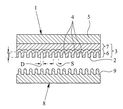
2s to the drawing. The sole figure shows
a very schematic sectional elevation of a proposed stamping tool and a
work piece structured therewith.
3o In a highly simplified sectional elevation, the figure shows a proposed
stamping
tool 1 with a structured, i.e. profiled or relief like stamping surface 2. The
stamping surface 2 is formed by a flat side of a surface layer 3, which is
provided
with open hollow chambers 4 produced by anodic oxidation.
CA 0240720912002-10-23
-4_ ..
In the illustrative example, the surface layer is applied to a support 5 of
the
stamping tool 1. For example, the surface layer 3 is applied to the support 5
by
plasma coating. But the surface layer 3 can also be formed directly by the
support
S, and thus be a surface area of the support 5.
s
It is understood that the surface layer 3 can also be deposited on the support
S
using other methods.
In the illustrative example the surface layer 3 preferably consists of
aluminium
io which is applied to the support S especially via plasma coating and adheres
well
to the support 5 preferably made of metal, especially iron or steel.
The surface layer 3 is oxidised anodically at least partially in the
illustrative ex-
ample to the depth of a covering layer 6, whereby the hollow chambers 4 are
is formed in the surface layer 3. The hollow chambers 4 are formed immediately
and/or without any model or pattern, i.e. the arrangement, distribution, form
and
the like of the hollow chambers 4 - as opposed to electrolytic machining - is,
thus, at least essentially independent of the surface shape and the proximity
of
the cathode (not shown) used in oxidation. Moreover, according to the
invention,
2o the "valve effect", namely the occurring, independent formation of hollow
cham
bers 4 during oxidation or anodisation of the surface layer 3, - at least in
par
ticular in the so-called valve metals - is used. This immediate or undefined
for
mation of the hollow chambers 4 does not preclude an additional (before or
after)
formation or structuring of the stamping surface 2 or the hollow chambers 4 by
2s means of a negative form.
Depending on how completely or how deeply the surface layer 3 is oxidised, or
whether the surface layer 3 is formed directly by the support 5, the surface
Iayer
3 can correspond to the oxidised covering layer 6. In this case, for example,
the
3o intermediate layer 7, which is comprised of aluminium in the illustrative
example
and which promotes very good adhesion between the covering layer 6 and the
support 5, can be omitted.
For example, according to an alternative embodiment, the uncoated support 5
can
3s be oxidised anodically on its surface forming the stamping surface 2 by
forma-
1
CA 02407209 2002-10-23
- 5 -
tion of a porous oxide layer or hollow chambers 4. This is possible for
example
for a support 5 made of iron or steel, especially stainless steel. In this
case the
surface layer 3 then corresponds to the covering layer 6, i.e. the oxidised
layer.
s Aluminium and iron or steel, especially stainless steel, have already been
named
as particularly preferred material, used at least substantially for forming
the ano-
dically oxidised surface layer 3 or the covering layer 6. However, silicon and
ti-
tanium as well as other valve metals for example can also be used.
to In the illustrative example the proportions in size are not presented true
to scale.
The stamping tool 1 or its stamping surface 2 preferably has a structural
width S
in the nanometre range, especially from 30 to 600 mm and preferably from 50 to
200 mm.
~s
The hollow chambers 4 or their openings have an average diameter D of essen-
tially 10 to S00 mm, preferably 15 to 200 mm and especially 20 to 100 run.
In the illustrative example the hollow chambers 4 are designed essentially
20 lengthwise, wherein their depth T is preferably at least approximately 0.5
times
the above-mentioned, average diameter D and especially approximately 1.0 to 10
times the diameter D.
The hollow chambers 4 are designed here at least substantially similarly in
shape.
2s In particular, the hollow chambers 4 are designed substantially
cylindrically. But
the hollow chambers 4 can also present a form deviating therefrom, for example
they can be designed substantially comically.
In general; the hollow chambers 4 can also have a cross-section varying in its
3o depth T in form and/or diameter. In addition to this, the hollow chambers 4
can
be designed substantially comically as a rough structure for example, and pro-
vided along their walls with many fine depressions (small hollow chambers) to
form a fine structure in each case.
' CA 02407209 2002-10-23
-6-
The hollow chambers 4 are preferably distributed at least substantially
uniformly
over the surface of the surface layer 3 or over the stamping surface 2.
However,
uneven distribution is also feasible.
s The hollow chambers or their openings are preferably distributed over the
stamping surface 2 with a surface density of 1O9 to 10''/cm2. In the
illustrative
example the surface density is substantially constant over the stamping
surface 2.
But the surface density can also vary partially on the stamping surface 2 as
re-
quired.
The area of the openings of the hollow chambers 4 is, at the most, preferably
50
of the extension area of the stamping surface 2. A sufficiently high stability
or
carrying capacity of the stamping surface 2 or the surface layer 3/covering
layer
6 is hereby achieved with respect to the high stresses arising during the
stamping.
is
In general, the form, configuration, surface density and the like of the
hollow
chambers 4 can be controlled by corresponding choice of the procedural condi-
tions during anodic oxidation. For example, with oxidation of aluminium under
potentiostatic conditions - with at least substantially constant voltage - an
at
20 least substantially even cross-section of the hollow chambers 4 is achieved
over
their depth T, i.e. an at least substantially cylindrical form. Accordingly,
the form
of the hollow chambers 4 can be influenced by varying the voltage. For
example,
galvanostatic oxidation - i.e. at an at least substantially constant current -
leads
to a somewhat conical or hill-like form of the hollow chambers 4, so that a
type
2s of "moth eye structure" or the like can be formed in this way. The surface
density
of the hollow chambers 4, i.e. the number of hollow chambers 4 per surface
unit
the stamping surface 2, depends inter alia on the voltage and the current
during
anodising.
3o As required, the hollow chambers 4 can vary in their form, depth and/or
surface
density over the stamping surface 2, especially partially, and/or be designed
only
partly on the stamping surface 2.
And, if required, the stamping surface 2 can also be modified before and/or
after
3s oxidation - creation of the hollow chambers 4 - for example via a
lithographic
p d
CA 02407209 2002-10-23
-'7-
process, etching and/or other, preferably material-stripping methods, for
example
to create a rough structure in the form of paths, ridges, areas with or
without
hollow chambers 4, large-surface bumps or depressions and the like on the
stamping surface 2.
Chemical sizing, especially by partial etching of oxide material, can also be
car-
ried out to modify the stamping surface 2 or the hollow chambers 4. In this
way
the surface ratio of the opening surfaces of the hollow chambers 4 to the
exten-
sion area of the stamping surface 2 can be varied or increased. It is
understood
io that other modifications of the stamping surface 2 or of the hollow
chambers 4
can also be made, depending on reaction time and intensity.
A particular advantage of the proposed solution is that the stamping surface 2
can
also be designed in a curved manner - for example cylindrically - or bulged -
for
Is example lenticular or hemispherical. In particular the stamping surface 2
can
have practically any shape at all. Compared to the prior art it is thus not
neces-
sary that the stamping surface 2 or the surface of the surface layer
3/covering
layer 6 is at least substantially even.
2o The figure also shows a work piece 8, likewise in a highly simplified, not
true-to-
scale sectional diagram, in the already stamped state, i.e. with a surface 9
already
structured by the stamping tool 1. Stamping takes places especially by the
stamping tool 1 being pressed with a corresponding stamping force onto the sur-
face 9 of the work piece 8 to be structured, so that the material of the work
piece
2s 8 flows at least partially into the hollow chambers 4. Here it is not
necessary that
the work piece 8, as illustrated diagrammatically in the figure, is designed
in a
monobloc manner. Instead, the work piece 8 can also present another type of
sur-
face layer or surface coating or the like, not illustrated here, which forms
the sur-
face, 9 and is structured or designed in a relief like manner by means of the
3o stamping tool 1.
Instead of the stamp-like embossing the stamping tool 1 can be unrolled with
cor-
responding shaping/form of the stamping surface 2 and/or the surface 9 to be
structured. By way of example the stamping surface 2 and/or the surface 9 to
be
CA 02407209 2002-10-23
_8-
structured can be designed in a curved manner - for example cylindrically - or
in
a bulged manner to enable reciprocal unrolling for structuring the surface 9.
Both a die stamping process and also a rolling stamp process can be realised
with
s the proposed solution.
Furthermore, the proposed solution can be used for embossing as well as closed-
die coining or coining. A corresponding abutment for the work piece 8 or a cor-
responding countertool is not illustrated for clarification purposes.
io
The proposed stamping tool 1 allows very fine structuring of the work piece 8
or
its surface 9. If needed the work piece 8 or the surface 9 can also be
profiled or
structured repeatedly, first with a rough structured stamping tool -
optionally
manufactured also in customary fashion - and then with the finer structured
pro-
is posed stamping tool 1. A lower stamping force is employed, especially
during
the second stamping procedure using the finer stamping tool 1 and/or, in an in-
termediate step, the surface 9 is hardened in order not to fully neutralise
the
rough structure produced at first stamping, but to achieve superposition from
the
rough structure and the fine structure of both stamping tools. Thus, it is
possible,
2o for example, to create on the surface 9 relatively large bumps of the order
of 0.1
to 50 ~,m each with several, relatively small protrusions, for example of the
order
of 10 to 400 nm, on the surface 9 of the work piece 8.
The proposed solution very easily and cost-effectively enables very fine struc-
2s turfing of the surface 9. Accordingly, there is a very broad area of
application. For
example, such especially very fine structuring can be utilised in anti-reflex
lay-
ers, for altering radiation emission of structured surfaces, in sensory
analysis, in
catalysis, in self cleaning surfaces, in improving surface wetability and the
like.
In particular, the proposed solution also extends to the use of work pieces 8
with
3o structured surfaces 9 that have been structured by use of the proposed
stamping
tool 1 for the purposes mentioned hereinabove.
In particular the proposed solution is suited for stamping synthetic materials
- for
example PMMA (polymethyl methacrylates), Teflon or the like, metals - for ex-
CA 02407209 2002-10-23
ample gold, silver, platinum, lead, idium, cadmium, zinc or the like, polymer
coatings - for example paints, dyes or the like, and inorganic coating systems
etc.
Expressed in general terms, an essential aspect of the present invention is
using a
s surface layer with hollow chambers formed by anodic oxidation as bottom die
or
upper die, to enable surface structuring in the nanometre range.