Note: Descriptions are shown in the official language in which they were submitted.
CA 02407960 2002-10-11
Doc. No. 18-40 CA Patent
System and Method for Direct Transmitter Self-Calibration
Field of the Invention
[0001] The instant invention relates to calibration of quadrature (I/Q)
modulators, and in
particular to self-calibration of a direct transmitter used in digital
communication system, as well
as in radar and instrumentation fields.
Background of the Invention
[U002] Digital communication techniques are by now the emerging standard in
almost all areas
of telecommunication. Digital communication is often based on a special class
of communication
signals, sent by a transmitter and received by a receiver, using digital
modulation techniques.
These techniques make use of a class of signal modulators, which perform
vector or quadrature
modulation. A vector-modulated or quadrature-modulated signal is an amplitude
and phase
modulated signal that is modulated according to in-phase and quadrature phase
components,
which define a phase vector. In vector or duadrature modulation, two
modulation input signals
independently modulate the in-phase (I) and quadrature (Q) components of a
carrier signal. For
proper operation, the I and Q channels of the modulator are ideally calibrated
to be equal in gain,
f. e. balanced, and 90° apart, f. e. in quadrature.
[0003) It is known that gain and phase imbalance between the I and Q channels
in a vector or
quadrature modulator degrade the overall communication link performance.
Although
compensation within a quadrature receiver for eliminating the performance
degradation due to
the phase imbalance is effective, the degradation due to the gain imbalance is
not to be
eliminated at the receiver in a straightforward manner. Ill addltloIl, ally DC
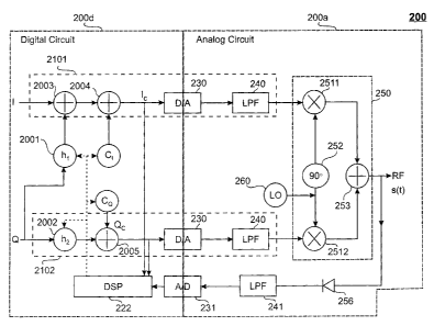
offsets possibly cause
a local oscillator (LO) signal to leak through the vector modulator, the LO
being part of the
vector modulator. In many cases, vector modulators designed to be fed I- and Q-
signals with a
given DC offset, for example 0.5 V. After fabrication of the vector modulator,
the optimal DC
offset optionally takes on values that are different from the designed value.
For example, the
optimal DC offset for the I-channel is 0.48V, whereas the optimatl offset for
the Q-channel is
0.52 V. Therefore, the expression "correcting for DC offset" has to be
understood as
"compensation for deviation from an optimal DC offset''.
CA 02407960 2002-10-11
Doc. No. 18-40 CA Patent
[0004] The leakage as well as the gain and phase imbalance distort the
transmitted signal, and
make it difficult to meet a given spectrum mask requirement. Therefore, it is
desirable to
eliminate or minimize imbalances and deviations from opfimurn offsets at the
transmitter.
Preferably, a calibration process is used to achieve this task.
[000] Given the importance of digital communication in today's media world, a
plethora of
studies have been devoted to estimating and correcting for errors in vector
modulators, and
improving performance of direct transmitters. Therefore, the instant invention
will be better
understood and highly appreciated, when viewed in the context of relevant
prior art.
[0006] Tuthill and Cantoni (1999 IEEE Int'1 Conf. on Acoustics, Speech and
Signal
Processing, Vol. III, pp.1621-1624) describe a method for compensation of the
imperfections of
reconstruction filters only. The proposed methodology is to adaptively control
the digital channel
filters to compensate for the reconstruction filter imperfections, such as
departure from linear
phase and from constant amplitude response, as well as gain and phase
imbalance between I and
Q filters. However, this methodology does not address the vector modulator
imperfections.
[0007] Leyonhjelm and Faulkner (IEEE 'mans. on Vehicular. Technology, Vol 44,
No.l, Feb.
199, pp. 95-102) address the use of a direct modulator for multiple channels.
The phase and
gain imbalances in transmit I and Q channels exhibit a frequency dependency,
and thus require
adjustment. The proposed technique is to add to each channel a lower side hand
(LSB) signal
that will destructively add with the one generated. However, a ChanIlel haS to
be free, when the
I~SB signal to be inserted is determined, a frequency down conversion of the
transmitted signal is
also necessary.
[0008] Hilborn, Stapleton, and Cavers (IEEE Trans. on Vehicular Technology,
Vol 43, No.2,
May 1994, pp. 223-233) propose a technique to compensate for both the
quadrature modulator
imperfections and the nonlinearities in power amplifiers. The technique to
derive both quadrature
modulator pre-distortion coeft7cients and amplifier lin earizer coefficients
is based on measuring
the signal power in a channel adjacent to the desired one. It is shown that
the pov~~er in the
adjacent signal is approximately a quadratic function of the modulator and
amplifier distortions.
However, a pre-selection filter is needed at the output port to reject the
transmitted signal and to
3
CA 02407960 2002-10-11
Doc. No. 18-40 CA Patent
look at an adjacent channel only. The technique works only when modulator and
amplifier
imperfections are small so that certain underlying approximations remain
valid.
[0009] Cavers and Liao (IEEE Trans. on Vehicular Technology, Vol. 42, No.4,
Nov. 1993, pp.
581-588.) propose a technique to compensate for direct modulator
imperfections. A power
detector is used to sample a modulator output signal, and by feeding the
modulator with a known
sequence of signals, coefficients for DC'. offset and gain and phase imbalance
compensation are
derived. This sequential technique adjusts first the DC offset and then the
gain and phase
imbalances. A series of tones with four different phases is used to derive the
required gain and
phase imbalance adjustment factors. A least-mean-square technique is used to
average the
coeft7cients obtained from several measurements, and to converge to a steady
state. The
adaptation and calibration is performed during non-transmission periods of
time. In addition, the
DC offset coefficients are calibrated by grounding the inputs of the vector
modulator. In this
case, measuring the output power of the modulator with a power detector is
difficult, and the
accuracy of the results is a function of sensitivity of a power detector and a
dynamic range of a
feedback system. Disadvantageously, it is necessary to make measurements with
no signal fed to
the vector modulator and thus requires a feedback loop {i.e. power detector
and analog-to-digital
converter) with high dynamic range operating during non-transmission periods
of time.
[0010] Cavers and Liao (Pros. of IEEE Vehicular 'technology Conference, May 19-
22, 1991,
pp.~78-583) propose a technique to be used at the receiver to compensate for
both transmitter
and receiver imperfections. A three-tap equaliser is used at the receiver in
either a decision
directed mode or reference aided mode. Although the authors claim that all the
modulator
imperfections are compensated, a modulator gain imbalance likely results in a
signal-to-noise
ratio degradation that is not likely recovered at the receiver. 1n addition,
transmitter DC offset
losses translate into local oscillator LO leakage which consumes transmit
power inefficiently as
opposed to power used for transmission of the desired signal. The quadrature
signals are possibly
recovered at the receiver even in the presence of modulator imperfections at a
cost of a likely
performance loss.
[001] Cavers (IEEE Trans. on Vehicular Technology, Vol. 46, No.3, August 1997,
pp. 707
716) also derives pre-distortion coeiticicnts from a solution of a set of
linear equations. This
4
CA 02407960 2002-10-11
Doc. No. 18-40 CA Patent
technique is iterative, and usually uses two or more iterations to result in
reasonable
performance. The approximations made in solving the linear equations are only
valid when
errors are small. Further, the technique is computationally costly. and
matrices are not likely to
be well conditioned. Thus, a matrix inversion algorithm necessary is likely to
be non trivial.
[0012] Ren and Wolff (1997 IEEE-MTT-S proceeding, June 8-13, 1997, vol. III,
pp. 1691-
1694) describe a technique to determine pre-distortion coefficients. The
technique relies on
demodulating the modulator's output signal and building a database of
correction factors for each
potential I and Q signal to be transmitted. However, this method relies on a
transmitter signal
demodulated in a feedback loop.
[0013] Yang, Vos and Cho (Proc. of IEEE Vehicular Technology Conference,
Atlanta, April
28-May l, 1996, Vol. II, pp.1317-1320) address gain and phase imbalance
effects in a direct
modulator. They present a correction algorithm, which is riot likely to be
intended for real time
implementations but as part of a calibration phase in a production line
instead. Phase and gain
imbalance pre-distortion factors are determined using a two-dimensional root
finding algorithm,
utilizing signal-to-image rejection ratio measured with a spectrum analyzer as
a feedback signal.
This method is not suitable for real time implementation nor does it
compensate for DC offsets.
[0014] Lohtia, Goud, and Engletield (IEEE PACRIM 1993 Conference Proceedings,
Victoria,
>\-Tay 19-21, 1993, Vol. II, pp. 447-450) defined a nonlinear model of the
vector modulator and
proposed a technique to assess five unknown model variables by solving a set
of five
independent nonlinear equations based on five output power measurements. The
set of nonlinear
equations is solved using a nonlinear root ftnding technique. However,
nonlinear modeling and
solving a set of nonlinear equations, possihly leads to convergence problems.
(UO1~J In U.S. Patent No 5,387,883, issued Feb. 7, 199 to Ueda, a duadrature
modulator
having controlled phase shifter is described. However, the modulator
compensates only for phase
imbalance. The modulator is fed with calibration signals during non-
transmission periods of
time.
[0016] In U.S. Patent No 5,293,406, issued March 8, 1994 to Suzuki, a
quadrature amplitude
modulator with distortion compensation is disclosed. Again, the modulator
works during non-
CA 02407960 2002-10-11
Doc. No. 18-40 CA Patent
transmission periods of time, and relies on the use of various calibration
signals. Furthermore,
sequential compensation is not likely to warrant full compensation due to a
correlation between
gain and phase imbalances.
[0017] In U.S. Patent No 5,663,691, issued September 2, 1997, to Kowalik et
al., an estimator
for estimating an operating defect in a quadrature modulator, and a modulation
stage using the
estimator, are described. In this approach, the instantaneous output signal
power is multiplied
with the base band I and Q signals, the product is integrated to get an
indication of the phase
imbalances and DC offsets. However, there is no amplitude imbalance
compensation and/or
estimation. Most likely this technique utilises a manual calibration process.
[0018 It would be highly advantageous to provide a system and method that
overcome the
limitations and drawbacks of the prior art.
Object of the Invention
[0019] It is an object of the instant invention to provide a calibration
method of determining
pre-distortion coefficients to be applied to in-phase (1) and duadrature (Q)
signals feeding a
direct transmitter in order to maximize local oscillator (LO) suppression, as
well as to maximize
unwanted sideband suppression, the pre-distortion coefficients being used to
adjust the relative
phase and gain between the I and Q signals as well as DC offsets of the I and
Q signals, the
proposed technique not involving any approximation on the values of the pre-
distortion
coefficients.
[0020) It is also an object of the instant invention to provide a calibration
method that is fully
adaptive, thus allowing the use of a low dynamic range in the feedback
circuit.
(0021) It is further an object of the instant invention to provide a
calibration method that is
able to track and correct changes over times as they occur
[0022] It is another object of the instant invention to provide a calibration
method for adaptive
determination of gain and phase imbalances and DC offsets, using a least-mean-
square (LMS) or
recursive-least-square (RLS) based process, and using a truly mapped linear
model without any
approximation.
6
CA 02407960 2002-10-11
Doc. No. 18-40 CA Patent
[0023) It is further another object of the instant invention to provide a
calibration method for
adaptive estimation based on an algorithm, which does not rely on contiguous
samples of the
output signal power, thus allowing for a low sampling rate.
[0024] It is yet another object of the instant mventlon to provide an
apparatus for providing a
carrier modulated signal, in which the I and Q channel signals have been pre-
distorted for local
oscillator as well as unwanted sideband signal suppression the pre-distortion
coefficients
obtained applying an algorithm based on a truly mapped linear model without
any
approximations.
Summary of the Invention
[0020 In accordance with an aspect of the instant invention, there is provided
a method for
self calibrating a vector modulator. The method includes a step of determining
pre-distortion
coefficients in dependence upon an in-phase signal, a quadrature signal. and
an output envelope
of an RF signal. 'The method further comprises the steps of transforming a
value representative of
an output envelope represented in a nonlinear domain into a value
representative of the output
envelope represented in a linear domain, determining a parameter vector x as a
solution of a
linear equation within the linear domain, and determining the pre-distol-tion
coefficients from the
parameter vector x.
[0026] In accordance with another aspect of the instant invention, there is
provided a
compensating quadrature modulator for self=calibrating a vector modulation
process, the
compensating quadrature modulator comprising: an I-signal transmit chain for
pre-distorting and
transmitting an in-phase signal, a Q-signal transmit chain for pre-distorting
and transmitting a
quadrature signal, a vector modulator fir modulating the in-phase signal and
the quadrature
signal and for providing an analog RF output signal, an envelope detector
coupled to the vector
modulator output for detecting the. analog RF output signal and for providing
an analog envelope
of the RF output signal, an analog-to-digital converter coupled to the
envelope detector for
receiving the analog envelope RI' output signal and for converting the
received signal into a
digital envelope of an RF output signal, and a digital signal processor for
determining at least a
digital signal pre-distortion coefficient by which signals in one of the I-
signal transmit chain and
the Q-signal transmit chain are pre-distorted, the digital signal processor
being coupled to the
7
CA 02407960 2002-10-11
Doc. No. 18-40 CA Patent
analog-to-digital converter, and being coupled to the I-signal transmit chain
and the Q-signal
transmit chain. The digital signal processor comprises circuitry for
performing the steps of
transforming a value representative of an output envelope represented in a
nonlinear domain into
a value representative of the output envelope represented in a linear domain,
determining a
parameter vector x as a solution of a linear equation within the linear
domain, and determining
the pre-distortion coefficients from the parameter vector x.
Brief Description of the Drawings
[0027] Embodiments of the instant invention will now be described in
conjunction with the
following drawings, in which
[0028] Figure 1 displays a titnctional block diagram of a prior art direct
digital transmitter
(DDT) 1;
[0029] Figure 2 displays functional block diagram of a compensating quadrature
modulator
according to the instant invention;
[0030] Figure 3 shows a flow chart for an LMS-based implementation of an
algorithm
according to the instant invention;
[0031] Figure 4 shows a flow chart for an RLS-based implementation of an
algorithm
according to the instant invention;
[0032] Figure S displays BER performance curves of a simulated QPSK
communication
system with and without compensation according to the instant invention;
[0033] Figure 6 shows a transmit spectrum of a quadrature-modulated signal
without
correction of gain/phase imbalances and DC offsets; and
(0034] Figure 7, shows a transmit spectrum of a quadrature-modulated signal
with correction
of gain/phase imbalances and DC offsets according to the instant invention.
8
CA 02407960 2002-10-11
Doc. No. 18-40 CA Patent
Detailed Description of the Invention
[0035) The instant invention is now described in detail. In particular, the
instant invention will
be demonstrated with an exemplary model developed for a square law power
detector. A person
of skill in the art will appreciate that the instant invention is easily
modified using models based
on other type of envelope detectors, such as for example linear envelope
detectors and
logarithmic envelope detectors. It is understood that power is a
representation of the envelope of
a signal.
[0036] Referring to Figure l, a functional block diagram of a prior art direct
digital transmitter
(DDT) 100 is shown. The direct digital transmitter (DDT) 100 comprises a
digital signal
generator (DSG) 110, which generates an in-phase (I) and a quadrature (Q)
signal. Two transmit
chains. the I-signal chain 1101 and the Q-signal chain 1102, each comprises a
Digital-to-Analog
(D/A) converter 120, a low pass filter (LPF) 130, and an amplifier 140. The I
and Q signals are
fed through the I and Q signal chains to a vector modulator 150. Further, a
local oscillator (LO)
160 is connected to the vector modulator 150. A signal generated by the local
oscillator is fed to
the vector modulator 150, where it is split into two orthogonal signals in the
splitter/phase-shifter
152. A mixer 1511 multiplies the in-phase signal I by the LO-si~~nal, whereas
a second mixer
1512 multiplies the quadrature signal Q by a 90°-shifted LO signal. The
mixed signals are then
summed in the adder 153 to form an RF output signal. Of course, the design of
the vector
modulator as described above constitutes only one specific design of the
vector modulator. A
person of skill in the art easily envisions other designs for the vector
modulator. For example
instead of phase shifting the LO by 90°, the Q signal is shifted bs
90°. Further alternately, the I-
signal LO is phase shifted by -45° and the Q-signal LO is phase shifted
by 4~°. These
considerations also apply to vector modulators of the instant invention.
[0037] In order for the direct digital transmitter (DDT) 100 to perform
properly, the transmit
chains 1101 and 1102 are preferably essentially matched in gain and phase, and
their DC offsets
are preferably such as expected by the vector modulator 150. In addition, the
splitter/phase
shifter 152 has to provide a 90°-phase shift and the mixers 1511 and
1512 responses have to be
matched in gain and phase. These conditions are difficult to achieve,
especially when the direct
digital transmitter 100 is operated at microwave frequencies.
9
CA 02407960 2002-10-11
Doc. No. 18-~l0 CA Patent
[0038] In practice, the input signals fed to the vector modulator ISO are
tuned to compensate
for imperfections in the direct digital transmitter (DDT) 100. The tuning
involves adjusting the
relative amplitude and phase of the I and Q signals and adjusting the DC
offset of the I and Q
signals. The tuning represents a calibration process. 'fhe adjustment is
optionally done manually,
if a single calibration process is sufficient for proper functioning of the
DDT. The adjustment is
optionally automated for frequent or in use calibrations of the DDT.
Alternately, the tuning is
achieved by pre-distorting the I and Q signals in the digital signal generator
to achieve same
results.
[0039] Referring now to Figure ?, shown is a functional block diagram of a
compensating
quadrature modulator 200 according to the instant invention. The compensating
quadrature
modulator 200 corrects I and Q signals for gain/phase imbalances and DC
offsets. The correction
for gain/phase imbalances and DC offsets represents a calibration process. The
compensating
quadrature modulator comprises a digital circuit 2(?Od, an analog clrcult
200x, as well as an I-
signal transmit chain or I-channel 2101 and a Q-signal transmit chain or Q-
channel 2102. The l-
and Q-channels extend across the digital and analog circuits 200d and 200x.
Gain and phase of
the Q-channel relative to the I-channel are denoted as a and ø , while C', and
C.'~, are DC
offsets of the I and Q channels, respectively. Gain and phase corrections for
the Q-channel are
achieved by scaling the Q-channel signal by a factor h, and corrected for DC
offset by C~, . The
I-channel is offset by a scaled Q-channel signal. the scaling factor being 1y
., and corrected for
DC offset by C.', .The factors tai and y~, are defined as 11, ----- tan~~~ and
h, =l~acos~~).
[0040] The I-signal and Q-signal are provided to the 1-channel and to the Q-
channel,
respectively. 'hhe signal Q is split. and multiplied by the factor h, in the
multiplier 2001. This
modified Q-signal is added to the I-signal in the adder 2003. The now modified
I-signal is
corrected for DC offset by subtracting C', in the adder 2004. The result of
these operations is a
pre-distorted signal 1~.. In the Q-channel, the Q-signal is multiplied by the
factor h, in the
multiplier 2002. From the multiplied signal the component C.,'~, is subtracted
in the adder 2005,
resulting in a pre-distorted signal p~. . The pre-distorted signals are passed
through digital/analog
converters (D/A) 230, lo~v-pass filters (I,PF) 240, and are fed to vector
modulator 250.
CA 02407960 2002-10-11
Doc. No. 18-40 CA Patent
Optionally, the pre-distorted signals are amplified in an amplifier (not
shown) before provided to
the vector modulator 250. Further, a local oscillator 260 is coupled to the
vector modulator 250.
A splitter/phase shifter 252, mixers 2511 and 212, and an adder 253 operate in
a similar fashion
as those described for the vector modulator 1~0. The vector modulator 2~0
produces an RF
signal s(t), part of which is fed through a feedback circuit consisting of an
envelope detector
coupled to the vector modulator, the envelope detector shown as a diode 2~6,
an LPF 241, an
analog-to-digital converter 231, and to a digital signal processor (DSP) 222.
Optionally, an
ampliFer is integrated into the feedback (not shown). Also fed to the DSP 222
are the pre-
distorted signals l~. and U~ . The DSP 222 functions as a parameter estimator,
and generates the
coefficients C, , C~~" l?, and h, . Thus, the compensating quadrature
modulator 200 allows for
adaptive determination of gait~/phase imbalances and DC offsets, and adjusts
the correction
factors according to the current conditions of the analog circuit 200x. Thus,
the circuit is able to
take into account variations in ambient temperature and the like occurring
during circuit
operation. The compensating quadrature modulator 200 operates as a self-
calibrating device.
[0041] The principles of the layout of the digital circuit 200d of the
compensating quadrature
modulator 200 are apparent when analyzing underlying concepts for circuit
design. In the
following, a mathematical model, on which the instant embodiment is based, is
derived. A
carrier-modulated signal ,s(!) with gait~/phase imbalances and DC offset
distortion is modeled as
follows:
s(t) _ (1 (~) + C, )cos(a~t) - a~Q(t) + C~_, )sin(<ot + ~) (1)
[0042] In Equation l, 1(tj and ~7(t) represent the I and Q modulating signals,
and ~ denotes
the carrier frequency. As introduced above, a and ~ represent the total gain
and phase
imbalances between I and Q channels, while C', and C'~,are total DC offsets in
I aIld Q channels,
respectively. These imbalances and offsets are present in both the transmit
chains and the vector
modulator. Using a trigonometric identity. Equation I is expressed as
s(t) = U(t) cos(~~t) -1l'(t) sin(~t) (2)
Here, U(t) and V(t) are defined by
CA 02407960 2002-10-11
Doc. No. 18-40 CA Patent
U(t) _ (1(t) + C, ~- a(Q(t) + CL, ~sin(gS)
(3)
~(t) = a(Q(t) + C" )cos(~)
(0043) Based on the definitions given in Equations 1-3, a method for
determining the gain and
phase imbalances a and ~ , as well as the DC offsets C', and C~, is described
below. To this
end, the instantaneous output power p(t) of the vector modulator, which is
defined as
p(t) = U' (t) + L'' (t) (4)
is expressed in terms of U(t) and t'(t), and after straightforward
manipulation is written as
p(t) = I' (t) + (2C, - 2aC" sin(r~)~I(t) - 2a sin() I (t )0(t)
+ (2a2C~, - 2aC', sin(~)~O(t) + a'0' (t) (5)
+ ~C; + a''C~, - 2aC,C'" sin())
[0044) Considering N sample measurements with a sampling interval of 0z, ~z
defining the
time elapsed between measurement samples, and assuming that a measurement
circuit has again
G, it is possible to express the r~'~' sampled power measurement p(n) , with 1
S rr <_ h' , as
p(n)=G'p(n)+ w(n)+~S
[0045] In Equation 6, ~n(n) represents measurement noise, including thermal
noise in the
circuit and quantization noise. The thermal noise is generally modeled as
white zero-mean
Gaussian noise, whereas the quantization noise is generally modeled as a white
zero-mean
uniformly distributed noise. Further, in Equation 6, represents the DC bias in
the measurement
circuit. The measurement gain (i is introduced to account for gain uncertainty
in the
measurement circuit.
(0046) For further description, it is helpful to make use of an average
operator E{ } . The
average operator E{ } returns an average value of a set of v(n) variables,
when operating on
v(n) , indicated as E{v(n)~ . Applying the average operator to the power
measurement p(n) then
results in an average power measurement or mean power measurement ~~
1?
CA 02407960 2002-10-11
Doc. No. 18-40 CA Patent
~n - E1P(n)l
= E {I z (n)x, + I(n) x2 + I (rr)Q(n)x; + Q(n)xa + Q' (ra jxs + x~ + ~ + w(n)}
(7)
_ ~r x~ + f~~ xz + Yr3 + f~oxa + ~c~ xs + x6 + 8
[0047] In Equation 7, the following variables denoting the result of an
averaging operation
have been introduced: fir, = E~I(n)~, ,u~, = E{Q(n)~, ~; = E{I' (n)}, ~~; =
E{Q' (n)} and
y = E f I(n)Q(n)}. Further, x";1 <_ n <_ 6, are components of a ''gain
vector'' x defined as x, = G ,
x, _ ~2C, - 2aC~, sin(~)~G , x; _ -2a sin(~)G , x, _ ~2a 2C~, - 2aC', sin(~))G
, xs = a'G , and
x6 = (C; +a~C~, -2aClC~, sin(~))G .
[0048] When subtracting the mean power measurement ~~ from the power
measurement
p(n) , an AC-coupled power measurement p~ (n) is obtained. The AC-coupled
power
measurement is therefore given as
Po (n) = P(n) - ~~ = a ~ (n)x + w(n) (8)
[0049] In Equation 8, the superscript "M' as usual denotes a matrixlvector
transpose, and the
vectors a(n) and x are defined as
I~(n)_~i ~xn
I (n) - ~LLI X,
a(n) = 1 (n)Q(n) - y ; x = x ~ .
Q(n) - fro xa
O' (n) - ay, xs
The vector x now represents a five-dimensional parameter vector with the
components
x" ;1 5 n S 5 , as defined in the contest of Equation 7. 'The vector a
represents a DC-corrected
vector of components for the I and Q channel values, intensities, and cross
coupling.
(0050) The procedure outlined above allows one to transform a nonlinear
equation, Equation 5.
into a linear equation, Equation 8. A closer inspection reveals that Equation
5 is nonlinear in
C, , C~, , a, and ~, whereas Equation 8 is linear in x" ;1 <_ n _< 5 .
Therefore, in order to calculate
13
CA 02407960 2002-10-11
Doc. No. 18-40 CA Patent
the pre-distortion coefficients a, ~, C, , C.'~, , the linear Equation 8 is
solved to result values for
x";I < n < 5, from which then the pre-distortion coefficients are obtained.
[0051] The derived linearization process simplifies the determination
procedure for the pre-
distortion coefficients. Given Equation (8), the problem is reduced to
estimating the unknown
parameter x from the two observable sets ~a, (n)~ and ~po (n~} . A least-
square (LS) based
technique is used to perform this task in the present exemplary embodiment.
Optionally,
different mathematical techniques are used to obtain a solution for Equation
8.
[0052] The above analysis is based on correlated I and Q signals having non-
zero means and
equal or unequal powers. Possibly, the I and Q signals are uncorrelated, with
zero-means and
equal power. In this case, one has y = ,tt, = Ct~, = 0 and 6= a-" . Thus, the
case of uncorrelated
Q and I signals is a special case of correlated I and Q signals, and the above
derived formulation
is therefore applicable to uncorrelated signals as well.
[003] A method for determining the parameter vector x is outlined below. It is
helpful to
define an estimation error as
e(n) = po (n) - a' (n)x, for n =1,2, ~ ~ ~ 1f (9)
Given a corresponding error vector a = (ell), e(2), ~ ~ ~, e(~V~)t ~, and a
measurement vector
P = ~Po (1), po (2)~ "' > po (N)~r . the sum of the squared errors is written
as
s(x)= ~~e(n)~~ =(p-Aa)T(p-Ax) (10)
n=I
[004] In Equation 10, A is a 5-by-N matrix A = (a(1), az(2), ~ ~ ~, a~l~'~)t
~, formed by DC-corrected
vectors a(n); 1 S n 5 l~' . In a least square (LS;) method used to solve
Equation 8, the parameter
vector x is chosen to minimize the sum of the squared errors. An LS solution
to the above
problem is found in standard textbooks, see for example S. Haykin, Adaptive
Filter Theory, 3~'I
Edition, Prentice-Hall, New Jersey, 1996. 'the LS solution is given in
equation 1 I .
l4
CA 02407960 2002-10-11
Doc. No. 18-40 CA Patent
x - (A TA~_1 ATP (11 )
[0055] Haykin has demonstrated that the above estimate of x is a best linear
unbiased estimate,
when the measurement noise w(rt) is a zero-mean white noise. Since the
measurement noise in
cases, to which the instant invention applies. is most likely a zero-mean
white noise, the LS
solution is favorably applied in the instant invention.
[0056) Having obtained x, provided are values for the gain/phase imbalance
parameters a and
~ , and the DC offset parameters C, and C~, , which in turn are utilized to
compute the pre-
distortion coefficients for local oscillator and undesired sideband
suppression. The values are
provided according to the definitions of x;. Corresponding solutions are given
in Equations 12-
14:
(12)
~ = sin-' - ~'' (13)
2 x,x;
C, 2G - 2a sin(~)G ' s, (14)
C~, - 2a sin(~)G 2a'G x~
The pre-distorted I and Q channel signals, denoted as I~. (r~) and O~ (n~, are
obtained from the
inverse system to the signal model of Equation 3:
I~ (n) 1 - a sin() ' I (n) C,
(15)
O. n 0 a cos n
(~) ~( )
The inverse matrix in Equation 15 is written as
r1 -asin(~)~ ' - ~ 1 tan()
I' J ( 16)
0 acos(ø) 0 1/acos(~
CA 02407960 2002-10-11
Doc. No. l8-40 CA Patent
and the following set of equations to determine the pre-distorted signals
I~.(n) and Q~.(n) results
from Equations 15 and 16:
I~.(n)= I(n) +tan(~)~ Q(n)-C,
(17)
O~. (n ) _ ~1/a cos(~)~ ~ Q(n ) - C~,
[0057] The relations for l~.(n) and Q~.(n) derived in Equation 17 constitute a
basis for the
design of the digital circuit 2004 of the compensating quadrature modulator
200, the digital
circuit 2004 modulating the I(t) and Q(t) input signals. According to the
instant embodiment,
the pre-distorted signals, l~.(n) and O~ (n) , are converted to analog
signals, filtered and applied
to the vector modulator of Equation I .
[008] To verify that the above pre-distortion indeed removes the effects of
any gain/phase
imbalances and DC offsets at the modulator output, in the set of linear
equations given in
Equation 3, I(n) and Q(nj are replaced by l~. (n~ and O~.(n), yielding
U(n) 1 -asin(~) I~.(n) + ~C,
V(n) 0 acos(~) Q~.(n), ,Ct,
1 - a sin() 1 - a sin(ø) ~ I (n) C,, Cr
0 a cos(~) 0 a cos(~) Q(n) C« C~,
(18)
1 - a sin() 1 - a sin() ~ ~ I (n)
0 a cos(~) 0 a cos(~) ~Q(n)
I(n)
Q(n)
It follows from Equations 2 and 18 that after the pre-distortion, the effects
of any gain/phase
imbalances and DC offsets are eliminated from the output of the vector
modulator.
(0059] Equations 11-14 and 17 form a basis for a procedure for correcting
gain/phase
imbalance and DC offset. It is possible to solve Equation 11 directly by first
taking a set of N
measurements, and then carrying out matrix muItiplications and inversion. The
direct
implementation is suitable for a stationary environment where the gait~/phase
imbalances and DC
16
CA 02407960 2002-10-11
Doc. No. 18-40 CA Patent
offsets do not change rapidly, and an adaptiveness other than a high
adaptiveness is possibly
sufficient. However, if the gain/phase imbalances and DC offsets change
rapidly with time, it is
advantageous to have an adaptive implementation. Although the present
implementation is
possibly operated repeatedly' from time to time to update the pre-distortion
coefficients according
to changes of the gain/phase imbalances and DC offsets. preferred adaptive
solutions are for
example a least-mean-square (LMS) process, which is suitable for high-speed
transmission
systems; and a recursive least-squares (RL,S) process, which, compared to the
LMS process,
performs favorably in terms of convergence and residual error but which is
accompanied by an
increase in computational cost.
[0060) Referring to an embodiment of the instant invention, shown is in Figure
3 a flow chart 3
for an LMS-based implementation of a process according to the instant
invention. In this process,
the parameter vector x is obtained over time in an iterative fashion. For each
x, a set of pre-
distortion coefficients a , ~ , C-', and G'~, is calculated according to
Equations 12-14. In a first
step 301, relevant parameters are initialized. Preferably, at the initial
stage. n = 0, components of
the initial parameter vector x(0), x, (0);1 <_ l <_ S , as well as other
auxiliary parameters (AP) are
initialized with an initial value, the initial value being in the form of a
zero value, thus
x, (0) _ ,u, ~0) _ ~r~, (0) _ ~; ~0) _ ~~, (0) = a-;, (0) = y(0) = 0 .
Further. a step size Et is defined,
preferably in dependence of a total power value ~i, r1 being the power in the
DC-corrected
component vector a(n), such that 0 < ,u < 2/~7 , and an increment value i; is
selected, ~ being a
small positive number in the range of 0 < ~ 5 0.01 . In a next step 302, the
interval counter n is
incremented as i7 = n + 1. A power measurement p(r~) is taken, step 303, and
auxiliary parameters
(AP) are calculated, step 304. The AI' are determined according to the
following set of
equations:
17
CA 02407960 2002-10-11
Doc. No. 18-40 CA Patent
W (n) _ ~(la(n)-f~r(n-I)~+frr(n-
I)
~~(n)=~(I~(n)-~;(n-1)~+a~(n-1)
Y(n)= ~(I~(n)~~~(n)-Y(nI)~+Y(n-1)
-
f~o(n)=~(~~(n)Wrn(n-I)>+frn(wl) (A I)
6u (n) _ ~(Q~ (n) )+ o'o(n - I)
- ~y(n- I)
~~(n) _ ~~P(n) - + Q~,(n - I)
6~(n-1)>
Next, the DC-corrected component vector a is formulated, step 30~. a being
defined in Equation
A-2
I2 (n) - ~i (n)
l~. (n) - p, (n)
a = l~.(n)O~.(n) - y(n) (A-2)
~~ (n) - f~« (r~)
~~ (n) - 6p (n)
An error a is computed, step 306, and the solution vector is updated, step
307. Equations
governing steps 306 and 307 are Equations A-3 and A-4, respectively.
a = (p(n) - 6p (n))- x' (n)a (
x(n+1)=x(n)+,cr~e~a (A-4)
After each iteration, a new estimate of x is obtained. Then, Equations 12-14
are used to compute
a set of a, ø, C~ and Cp which are used to t.ipdate the pre-compensation
circuit. The method
returns to step 302, and the cycle is repeated. It is apparent from the
present description that the
process according to the instant embodiment as outlined in flow chart 3 is a
self-calibration
method.
(0061] Referring now to Figure 4, shown is a flow chart ~ for an RLS-based
implementation of
a process according to the instant invention. In a first step 401, relevant
parameters are
initialized. Preferably, at the initial stage, n = 0, components of the
initial parameter vector x(0),
x, (0);l <_ i S 5 , as well as other auxiliary parameters (AP) are initialized
with a predetermined
18
CA 02407960 2002-10-11
Doc. No. 18-40 CA Patent
value in the form of a zero value, thus
x; (0) _ ,u, ~0) _ ,tt~, ~0) _ ~; ~0) = a~, (0) _ ~,'', ~0) = y~0) = 0 .
Further, a matrix T is initialized as 8-
~~U, with U denoting an identity 5X5 matrix and 8 being a small positive
constant, a constant l~~ is
chosen as positive number close to l, and an increment value ~ is selected., ~
being a small
positive number in the range of 0 < ~ <_ 0.01. In a next step 402, the
interval counter n is
incremented as n = n + 1. A power measurement p(n) is taken, step 403, and
auxiliary parameters
(AP) are calculated, step 404. The AP are determined according to Equation A-
1. The DC-
corrected component vector a is formulated, step 40~, as defined in Equation A-
2. In step 406,
the matrix T, vectors b and k, as well as parameter v are updated according to
conditions for
updating given in Equation A-5:
T(n ) _ ~''T(n -1 ) - k ~ b
b= ~.-' ~T~ (n-I)~ a
k=~l+a'b~~ ~b (A-5)
a = (p(n) - ay,(n)>- x~ (n -1)a
In step 407, a solution vector x is updated, following Equation A-6:
x(n)= x(n-I)+ ~~k (A-6)
After each iteration, a new estimate of x is obtained. Then, Equations 12-14
are used to compute
a set of a, ~, C'~ and C~ which are used to update the pl'e-COmpeIlSat10I1
CII'CUIt. The method
returns to step 402, and the cycle is repeated. It is apparent from the
present description that the
process according to the instant embodiment as outlined in flow chart 4 is a
self calibration
method.
[00G2] The methods described above are outlined for I and Q channel signals
that are possibly
correlated, with non-zero means and unequal powers. Alternatively, the I and Q
channel signals
are. uncorrelated, zero-mean and edual-powered. In this case, the following
relations for the
auxiliary parameters hold: y = ~.i, = ~ y, --- 0 , and 6= r~~, . Under such
circumstances, the
updating equations for y(n) , ,tr, (n) , allll ,cl~, (n) are removed from
Equation A-1, and the
19
CA 02407960 2002-10-11
Doc. No. 18-40 CA Patent
updating equations for 6; (n) and 6~,(n) in Equation A-1 are combined into one
single
equation.
[0063] Methods according to the instant invention are accurate methods for
determining pre-
distortion coefficients. The methods do not involve a step of approximation.
Quantization and
noise possibly affect precision of the pre-distortion coefficients. Precision
is possibly influenced
according to a choice of instrumentation for exercising the methods. However,
quantization and
noise do not affect the accuracy of the pre-distortion coefficients. The
methods according to the
instant invention are accurate per .re.
[0064] Self calibration methods according to first embodiment of the instant
invention have
been evaluated through computer simulations of a coherent quadrature phase
shift keying
(QPSK) communication system. In the present example, the vector modulator
output power was
sampled at a rate of 4 samples/symbol, and an additive white Gaussian noise
(AWGN) channel
model was used in the simulation. Essentially perfect symbol timing and
carrier synchronization
at the receiver was assumed to focus on the effects of gait~/phase imbalances
and DC offset
compensation process. The following parameter values were used for the
gain/phase imbalances
and DC offsets in the transmitter: a = 0. 95 , yfi = 5 ° , C~ _ -0. 0~
and CQ = 0. 0~ .
[0065] Referring now to Figure S, shown is a bit-error rate (BER) performance
of the QPSK
communication system with and without compensation according to the above
embodiment. The
BER were calculated as a ratio of 100 bit errors over a number of bits
transmitted. It is observed
that the gain/phase imbalances and DC offsets deteriorate the BER performance
while both
proposed compensation techniques eliminate their effects and restore the BER
performance to
acceptable levels. It is also noted that the gain/phase imbalances and DC
offsets impact more on
the BER performance as the ratio of energy per bit over noise power density (
Eh/~'" ) increases
since at low Eb/No the channel noise is dominant. The curves displayed in
Figure 5 illustrate
that the correction according to the above-described LMS and RLS processes
essentially restore
the BER value to the theoretically undisturbed value.
[0066] In another embodiment of the instant invention, instead of feeding pre-
distorted I- and
Q-signals to the digital signal processor, a set of known probing signals is
applied to the vector
CA 02407960 2002-10-11
Doc. No. l8-40 CA Patent
modulator, and the associated envelope of the output signal is measured. For
example, a trigger
signal is provided to the digital signal processor to inform the digital
signal processor that a
specific training sequence is sent, and at least a set Of known I- and Q-
signals or probing signals
is applied to the vector modulator. The probing signals are selected such that
Q-channel gain a,
Q-channel phase offset ~, as well as DC offsets C, and C'~ are obtainable from
a set of envelope
measurements of the modulated output generated by the probing signals. In the
subsequent
derivation, the following average-operator obtained values are used: ,u, =
E~l(t)~,
,u" = E{O(t)~, ~; = E{I' (t)}, ~~, = E~Q' (t)} and y = E~l(t)Q(t)}. Further,
the gain vector
components are now~ given as x" ;0 _< n <_ ~ , with individual terms x, = G ,
x, _ (2C, - 2aC" sin(~)~G , x3 = -2a sin(~)G , xa = (2a'C~, - 2aC, SIIl(~))G ,
xs = a'G , and
xo = (C~ + a zC« - 2aC, C« sin(~))G .
The output power pt of the vector modulator in the case of known probing
signals is expressed as
p~ _ ~~ xi + flrx~ +Yr, + f~cn~ + ~co~; + xo (19)
When applying I(t) = O(t) = 0 to the vector modulator, and measuring an output
power p~, the
vector component .r~ becomes:
xo = po (20)
Setting I (t) = a eos(S2,t); Q(t) = 0 , a and S2 being known, and measuring a
power p~ , a value for
xr is obtained:
x, = 2(17, - xo)~a~ (21)
From Equation 21, and from the definition of x,, a value for the gain G is
calculated. Setting now
l>(t) = a cos(~t); I (t) = 0 , and measuring a power p, , a value for x;
becomes:
x; =2(pz -xo)~a' (22)
21
CA 02407960 2002-10-11
Doc. No. 18-40 CA Patent
The Q-channel gain a is then calculated according to Equation 12. When setting
I(t) = C~(t) = a cos(S2t) , and measuring an output power pj , a value for xj
is obtained;
x =(2(ps -xo)/a~)-xmxs (23)
3
The Q-channel phase offset ~ is then calculated according to Equation I 3. The
DC offsets C~ and
C~ are obtained from a set of four symmetrical pairs of I- and Q-signal inputs
each. Let
P.~ . ps I I I
1/4 1/2 1
Ps po
a = f~ J ~ b = f~c_> ; P a-7 = ~ P H-~ i = ; D =
Pc, pio I/4 -I/2 1
so xo
P~ , pn I -1 1
Providing the four symmetrical input signal pairs (1,0), (1/2,0). (-1/2,0),(-
I/0) and measuring the
power outputs p" ;4 <- n <_ 7 , Equation 24 is obtained:
(24)
D~a=P,_7
Similarly, providing the four symmetrical input signal pairs (0, I ). (0,1
/2), (0,-I/2),(0,-1 ) and
measuring the power outputs p";8 5 n <_ 1 I , Equation 25 is obtained:
D' b = Ps-a (25)
From the solutions of Equations 24 and 25, which result in the vector
components of n and b, the
DC offsets C, and C~ are obtained as
C,~, _ -,ct;,. ~2~ ~ ; with subscript X = I or Q (26)
[0067] Referring now to Figure 6, shown is a transmit spectrum of a quadrature-
modulated
signal without correction for gait~/phase unbalances and DC offsets. Besides
the main signal,
there are unwanted signals, causing distortion of the original signal.
Referring now to Figure 7,
shown is a transmit spectrum of a quadrature-modulated signal with correction
for gain/phase
imbalances and DC offsets according to the other embodiment of the instant
invention. The
sidebands due to DC offset and gaiuphase imbalance are effectively suppressed,
resulting in a
22
CA 02407960 2002-10-11
Doc, No. 18-40 CA Patent
reduction of noise and overall signal distortion, enhancing the signal
quality. LO leakage and
image suppression are improved by at least 20 dB. Figures 6 and 7 illustrate
how a method
according to the instant invention leads to an improvement of a transmit
spectrum.
[0068] The methods according to the instant invention avoid a use of
approximation on the
values of the pre-distortion coefficients and are thus applicable to a wide
range of distortions.
The proposed methods are truly adaptive to cope with time-induced variation in
direct
transmitter's performance. The instant invention is applicable to wireless
communication
systems, and particularly to broadband transmission systems in the ~tm- and mm-
wave range.
(0069) Although the instant invention has been described with respect to
specific embodiments
thereof, various changes and modifications are optionally carried out by those
skilled in the art
without departing from the scope of the invention. Therefore, it is intended
that the present
invention encompasses such changes and modifications as fall within the scope
of the appended
claims.
23