Note: Descriptions are shown in the official language in which they were submitted.
CA 02408491 2002-11-08
WO 01/86811 PCT/USO1/14376
-1-
CIRCUIT SIMULATING A DIODE
This application is a continuation-in-part of co-pending application
Serial Number 09/059,968 filed April 14, 1998 by the same inventor.
Field of the Invention
This invention relates to a circuit which behaves like a diode in the
sense that it conducts current in one direction and blocks current in the
opposite
direction. More specifically, the invention relates to a circuit simulating a
diode
without disadvantages of an actual diode.
Background of the Invention
Conventional p-n junction diodes and Schottky barrier diodes are
associated with a forward voltage threshold. More particularly, an ideal diode
would conduct a current in one direction without power loss and would block a
eurrent in the opposite direction. However, a practical (real) diode conducts
a
current in the forward direction, but only after a certain threshold voltage
is
reached. Furthermore, due to the internal resistance of an actual diode, an
additional voltage drop occurs depending on the values of the internal
resistance
and the current. The sum of the threshold voltage and the voltage drop caused
by
the internal resistance is referred to as a forward voltage drop (Vf) of a
diode.
In circuits having high forward currents, like power rectifiers and OR-
ing diodes in redundant power supplies, the power loss can be very high and
has
a significant impact on the efficiency of the circuit. Therefore, there is a
need for
a circuit which simulates the function of a diode in that it conducts current
in one
direction and blocks current in. the opposite direction, but has a low forward
voltage drop Vf in order to reduce power loss in circuits. In OR-ing diodes in
redundant power supply systems, the diode must switch off fast to avoid short
reverse current spikes if one power supply breaks down. However, there is no
need
for this diode to switch on very fast. There is a need for a circuit that
simulates a
CA 02408491 2002-11-08
WO 01/86811 PCT/USO1/14376
-2-
diode that switches on as well as off fast, i.e. at speeds as high as a few
hundred
kilohertz, for use in other applications such as for use as a rectifier in
switch-mode
power supplies.
Edlund, in U.S. Patent No. 4,417,164 issued November 22, 1983
discloses an electrical model for a unidirectional mechanical valve. Edlund
notes
that the properties of an actual diode for use in such a model has major
drawbacks
which differ from an ideal diode such as the presence of a voltage drop across
the
diode when it is conducting current. Further, an actual diode will not begin
to
conduct current until the voltage difference between the anode and the cathode
reaches a turn-on voltage of about 0.5 volts. Additionally, a diode does not
change
from a non-conducting to a conducting state immediately, but rather has a
finite
switching speed which depends in part on the rate of the change of the voltage
across the diode. A diode is adversely effected by the junction capacitance
between
the anode and the cathode. Accordingly, Edlund discloses a circuit as shown in
FIG. 1A incorporating a field effect transistor (n-channel enhancement MOSFET)
1 with drain and source terminals connected to input and output terminals A
and
K, respectively, as shown. A voltage comparator 2 has positive input 3 and
negative input 4 connected to the drain and source terminals of the MOSFET 1,
respectively, as shown. The comparator output 5 is coupled to the gate of the
MOSFET 1. The power supply for the voltage comparator is floating so that the
device is unaffected by the remainder of the electrical system.
It is known that in an n-channel device, the conventional flow of
drain current is in the positive direction - - that is, current flows from the
drain to
the source with a positive gate-to-source voltage. Typically the drain is
connected
to a higher voltage than the source. Further, it is known that an n-channel
device
has an integral reverse rectifier associated therewith. This intrinsic diode
is an
integral part of the device and is not a separate electrical component. In an
n-
channel device, the intrinsic diode effectively has an anode connected to the
source
and a cathode connected to the drain.
CA 02408491 2002-11-08
WO 01/86811 PCT/USO1/14376
-3-
FIG. 1B is provided by the Applicant for a patent for the present
invention for analysis of the actual operation of the prior art circuit of
FIG. 1A and
shows n-channel enhancement MOSFET 1 having an intrinsic diode la with its
anode connected to the source and its cathode connected to the drain. The
intrinsic diode 1a is enclosed within a circle with the symbol for the MOSFET
to
indicate that the intrinsic diode 1a is part of the MOSFET 1 and is not a
separate
electrical component.
The theoretical operation of Edlund's circuit in FIG. 1A is a follows:
when a higher voltage is placed on the drain then on the source, the output 5
of
voltage comparator 2 goes high and is input to the gate of the MOSFET 1.
Accordingly, the MOSFET 1 is controlled to conduct current from the terminal A
at a higher voltage to the terminal K at a lower voltage. On the other hand,
theoretically, during operation, when the terminal K is placed at a higher
voltage
than the terminal A, the output 5 of voltage comparator 2 goes low and is
input to
the gate of the MOSFET 1 in order to control the MOSFET to stop conducting
current. Theoretically, the MOSFET 1 will conduct current from terminal A to
terminal K when terminal A is at a higher voltage than terminal K. Further,
theoretically, in operation, the MOSFET 1 will not conduct current from
terminal
K to terminal A when terminal K is at a higher voltage than terminal A.
Accordingly, theoretically, Edlund's circuit simulates the action of a diode.
In actuality, however, the Applicant for a patent for the present
invention has identified a problem in the prior art: when Edlund's circuit is
actually constructed employing an actual MOSFET 1, it fails. FIG. 1B is
provided
to analyze the actual operation of the prior art circuit of FIG. 1A. More
particularly, when the voltage at terminal A is higher than the voltage at
terminal
K, the output 5 of the voltage comparator 2 goes high and is input to the gate
of
the MOSFET 1. The gate controls the MOSFET to conduct current from terminal
A to terminal K. On the other hand, when the voltage at terminal K is higher
than
the voltage at terminal A, the voltage comparator 2 delivers a low output
voltage
5 which is input to the gate of the MOSFET 1 in order to control the MOSFET 1
to
CA 02408491 2002-11-08
WO 01/86811 PCT/USO1/14376
-4-
stop conducting current and block current from terminal K to terminal A. Due
to
the integral reverse intrinsic diode la of the MOSFET 1, the MOSFET 1, in
practice,
actually conducts current from the high voltage at terminal K to the low
voltage at
terminal A. Accordingly, Edlund's circuit shown in FIG. 1A does not actually
operate to simulate the function of a diode because it does not take into
consideration the effect of the intrinsic diode 1a of the MOSFET 1 as
identified by
the Applicant for patent for the present invention.
Accordingly, there is still a need for a circuit that functions Iike a
diode in that it conducts current in one direction and blocks current in the
opposite
direction, however, has a low forward voltage drop. There is also a need for a
circuit that functions like a diode in that is conducts current in one
direction and
blocks current in the opposite direction that reduces power losses. There is
further
a need for a circuit that functions like a diode that switches on and off at
high
speeds.
Summary of the Invention
It is an object of the invention to provide a circuit which functions
like a conventional diode in that it conducts current in one direction and
blocks
current in the opposite direction.
A further object of the invention is to provide a circuit that simulates
the function of a diode that has a low forward voltage drop.
It is a further object of the invention to provide a circuit that
functions like a diode, but eliminates the threshold voltage of the forward
voltage
drop of a conventional diode.
It is still a further object of the invention to provide a circuit that
functions as a diode that detects if the circuit is malfunctioning.
Additionally, it is an object of the invention to provide a circuit that
functions as a diode that provides an indication of malfunctioning.
CA 02408491 2002-11-08
WO 01/86811 PCT/USO1/14376
-5-
It is another object of the invention to provide a circuit that conducts
current in one direction and blocks current in the opposite direction that
does not
have a threshold voltage.
It is an additional object of the invention to provide a circuit that
conducts current in one direction and blocks current in the opposite direction
that
reduces power losses.
It is still another object of the invention to provide a circuit which
functions as a diode which switches on and off fast.
It is yet another object of the invention to provide a circuit that
functions as a diode that switches on and off at speeds as high as a few
hundred
kilohertz.
It is a further object of the invention to provide a circuit that
functions as a diode for use as a rectifier in switch-mode power supplies.
These and other objects of the invention are accomplished by
providing a circuit for improving the switching performance of a three
terminal
switch comprising the three terminal switch having a source for electrons, a
drain
for electrons, and a control terminal having an internal capacitance between
the
control terminal and the source for electrons; and means for amplifying the
current
for modifying the charged state of said internal capacitance.
In a preferred embodiment, there is provided the means for
amplifying the current comprising a transistor.
In another preferred embodiment, there is provided a circuit with
two terminals A and K, which conducts current in one direction from terminal A
to
terminal K and blocks current in the opposite direction from terminal K to
terminal
A, comprising a voltage comparator, having a positive input, a negative input,
and
an output; and a three terminal means for switching current with a source for
electrons, a drain for electrons, and a control terminal controlled by a
voltage from
the output of the voltage comparator; the three terminal switching means
having
an internal capacitance between the control terminal and the source for
electrons
CA 02408491 2002-11-08
WO 01/86811 PCT/USO1/14376
-6-
associated therewith; and wherein the voltage comparator negates the effects
on
switching time of the switching means due to the internal capacitance.
The invention further contemplates a voltage comparator comprising
means for amplifying the current in order to negate the effects on switching
time
of the switching means due to the internal capacitance. Additionally, the
invention
employs means for amplifying the current comprising a transistor.
Also disclosed is a method of conducting current in one direction
from a terminal A to a terminal K and blocking current in a second direction
from
terminal K to terminal A, comprising: (a) comparing a voltage signal at a
positive
input of a comparator to a voltage signal at a negative input of the
comparator to
obtain an output voltage; (b) connecting a three terminal switch between
terminal
A and terminal K, wherein the three terminal switch has an internal resistance
associated therewith, an intrinsic diode associated therewith, and a source
for
electrons, a drain for electrons and a control terminal; (c) connecting the
output
voltage to the control terminal of the three terminal switch; (d) connecting
an
effective anode of the intrinsic diode to terminal A; (e) connecting an
effective
cathode of the intrinsic diode to terminal K; and (f) inputting voltage
signals to the
comparator by connecting the source of the three terminal switch to the
positive
input of the comparator, and connecting the drain of the three terminal switch
to
the negative input of the comparator.
The above and other objects, aspects, features and advantages of the
invention will be more readily apparent from the description of the preferred
embodiments thereof taken into conjunction with the accompanying drawings and
appended claims.
Brief Description of the Drawings
The invention is illustrated by way of example and not limitation in
the figures of the accompanying drawings in which like references denote like
or
corresponding parts and in which:
CA 02408491 2002-11-08
WO 01/86811 PCT/USO1/14376
-7-
FIG. 1A is an electrical model of a unidirectional mechanical device
employing a simulation for a diode in accordance with the prior art;
FIG. 1B is a diagram showing an intrinsic diode associated with a
MOSFET for analysis of the circuit of FIG. 1A;
FIG. 2 is a circuit simulating a diode in accordance with the invention
employing an n-channel enhancement MOSFET;
FIG. 3 is a circuit simulating a diode in accordance with another
embodiment of the invention employing a p-channel enhancement MOSFET;
FIG. 4 is the circuit of FIG. 2 with malfunction detection means and
a malfunction indicator added in accordance with another embodiment of the
invention;
FIG. 5A is a circuit simulating the function of a diode employing an
npn bipolar transistor in accordance with another embodiment of the invention;
FIG. 5B is a circuit simulating the function of a diode employing a
pnp bipolar transistor in accordance with another embodiment of the invention;
FIG. 6 is the circuit of FIG. 5A with malfunction detection means and
a malfunction indicator added in accordance with another embodiment of the
invention;
FIG. 7 is the circuit of FIG. 2 modified to employ an alternate voltage
comparator in accordance with another embodiment of the invention;
FIG. S is the circuit of FIG. 2 modified to employ another alternate
voltage comparator in accordance with yet another embodiment of the invention;
FIG. 9 is a circuit of the present invention similar to that of FIG. 7 and
showing a MOSFET with an intrinsic internal capacitance; and
FIG. 10 is a circuit of the present invention similar to that of FIG. 9
and showing a charging transistor for the internal capacitor of the MOSFET.
Description of the Preferred Embodiments
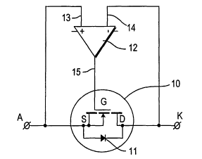
Refernng to FIG. 2, a circuit that functions like a diode in that it
conducts current in one direction from terminal A to terminal K and blocks
current
CA 02408491 2002-11-08
WO 01/86811 PCT/USO1/14376
_g_
in the opposite direction from terminal K to terminal A, but has a low forward
voltage drop is shown in accordance with the first embodiment of the
invention.
The circuit which conducts current in one direction from terminal A to
terminal K
and blocks current in the opposite direction from terminal K to terminal A
includes
a three terminal switching means 10 for switching current with a source for
electrons S, a drain for electrons D, and a eontrol terminal G. Further, the
three
terminal switching means 10 has an internal resistance associated with it and
an
intrinsic diode associated with it between the source and the drain. The
intrinsic
diode 11 is shown encompassed within a circle with the symbol for a MOSFET to
indicate that the intrinsic diode 11 is part of the three terminal switching
means 10
rather than a separate electrical component. The switching means l0 is
connected
between the terminals A and K.
The circuit of FIG. 2 further includes a voltage comparator 12 having
a positive input 13, a negative input 14 and an output 15. The output 15 is
connected to the control terminal G of the three terminal switching means 10.
The
source S of the three terminal switching means is connected to the positive
input
13 of the voltage comparator 12 and the drain D of the three terminal
switching
means 10 is connected to the negative input 14 of the voltage comparator 12.
The
intrinsic diode 11 has an effective anode connected to terminal A and an
effective
cathode connected to terminal K. Accordingly, in operation, the intrinsic
diode 11
enhances conduction from terminal A to terminal K and blocks conduction of
current from terminal K to terminal A. The internal diode 11 of the three
terminal
switching means operates to enhance the function of the entire circuit to
conduct
current in one direction from terminal A to terminal K and to block current in
the
opposite direction. Accordingly, the intrinsic diode 11 internal to the three
terminal switching means 10 is employed as a circuit element to enhance
operation
of the whole circuit rather than as in unfortunate side effect of a switch
that
degrades the operation of the circuit as in Edlund's prior art circuit of FIG.
1A.
In FIG. 2 the three terminal switching means is an n-channel
enhancement mode MOSFET. Accordingly, the intrinsic diode 11 has an effective
CA 02408491 2002-11-08
WO 01/86811 PCT/USO1/14376
-9-
anode connected to the source and an effective cathode connected to the drain.
As stated previously, the source is connected to terminal A and the drain is
connected to terminal K. Further, the source is connected to the positive
input 13
of the voltage comparator 12 and the drain is connected to the negative input
14
S of the voltage comparator 12.
In operation, employing an actual n-channel enhancement MOSFET,
the circuit of FIG. 2 functions as follows: when a higher voltage is at
terminal A
than at terminal K, the output 15 of voltage comparator 12 goes high turning
the
MOSFET 10 on to conduct current from the high voltage at the source to the low
voltage at the drain. Accordingly, current flows from terminal A to terminal
K. An
n-channel enhancement MOSFET will conduct current from the source to the
drain,
even though typically an n-channel enhancement MOSFET is used in circuits to
conduct current from the drain to the source.
However, when a higher voltage is at terminal K when compared to
the voltage at terminal A, the output 15 of voltage comparator 12 goes low and
is
input to the gate of the MOSFET 10 to turn off the current from terminal K to
terminal A. The intrinsic diode 11 assists in the operation of the MOSFET 10
by
blocking current flow from terminal K to terminal A because the cathode of the
intrinsic diode 11 is connected to terminal K and the anode of the intrinsic
diode
11 is connected to terminal A. Accordingly, the circuit of FIG. 2 functions as
a
diode in that it conducts current from terminal A to terminal K and blocks
current
from terminal K to terminal A. The intrinsic diode 11 of the MOSFET 10
enhances
the operation of the entire circuit rather than undermining the operation of
the
circuit as in Edlund's prior art circuit of FIG. 1A. Further, the threshold
voltage of
an actual diode is eliminated and the forward voltage drop is lower than that
for
a traditional diode and depends upon the values of the internal resistance
associated with the three terminal switching means 10 and the current through
the
three terminal switching means 10.
CA 02408491 2002-11-08
WO 01/86811 PCT/USO1/14376
-10-
The circuit of FIG. 2 may be modified to employ an n-channel
depletion MOSFETrather than the illustrated n-channel enhancement MOSFET 10.
Operation of the circuit is essentially the same.
FIG. 3 is a second embodiment of the invention employing a p-
channel enhancement mode MOSFET rather than the n-channel enhancement
mode MOSFET of FIG. 2.
The circuit of FIG. 3 includes a voltage comparator 22 having a
positive input 23 and a negative input 24 and an output 25. The output 25 is
connected to the control terminal G of the three terminal switching means 20.
The
source S of the three terminal switching means is connected to the positive
input
23 of the voltage comparator 22 and the drain D of the three terminal
switching
means 20 is connected to the negative input 24 of the voltage comparator 22.
The
intrinsic diode 21 of the switching means 20 has an effective anode connected
to
terminal A and an effective cathode connected to terminal K. Accordingly, in
operation, the intrinsic diode 21 enhances conduction from terminal A to
terminal
K and blocks conduction of current from terminal K to terminal A. The internal
diode 21 of the three terminal switching means 20 operates to enhance the
function of the entire circuit to conduct current in one direction from
terminal A
to terminal K and to block current in the opposite direction. Accordingly the
intrinsic diode 21 internal to the three terminal switching means 20 is
employed
as a circuit element to enhance operation of the circuit rather than as in
unfortunate side effect of a switch that degrades the operation of the circuit
as in
Edlund's prior art circuit of FIG. 1A. '
In FIG. 3 the three terminal switching means 20 is a p-channel
enhancement mode MOSFET. Accordingly, the intrinsic diode 21 has an effective
anode connected to the drain and an effective cathode connected to the source.
The drain is connected to terminal A and the source is connected to terminal
K.
Further, the source is connected to the positive input 23 of the voltage
comparator
CA 02408491 2002-11-08
WO 01/86811 PCT/USO1/14376
-11-
22 and the drain is connected to the negative input 24 of the voltage
comparator
22.
In operation, employing an actual p-channel enhancement MOSFET,
the circuit of FIG. 3 functions as follows: when a higher voltage is at
terminal A
S ~ than at terminal K, the output 25 of voltage comparator 22 goes low
turning the
MOSFET 20 on to conduct current from ~ the high voltage at the drain to the
low
voltage at the source. Accordingly, current flows from the terminal A to
terminal
K. A p-channel enhancement MOSFET will conduct current from the drain to the
source, even though typically a p-channel enhancement MOSFET is used in
circuits
to conduct current from the source to the drain.
However, when a higher voltage is at terminal K when compared to
the voltage at terminal A, the output 25 of voltage comparator 22 goes high
and
is input to the control terminal G of the MOSFET 20 to turn off the current
from
terminal K to terminal A. The intrinsic diode 21 assists in the operation of
the
MOSFET 20 by blocking current flow from terminal K to terminal A because the
cathode of the intrinsic diode 21 is connected to terminal K and the anode of
the
intrinsic diode 21 is connected to terminal A. Accordingly, the circuit of
FIG. 3
functions as a diode in that it conducts current from terminal A to terminal K
and
blocks current from terminal K to terminal A. The intrinsic diode 21 of the
MOSFET 20 enhances the operation of the entire circuit of FIG. 3 rather than
undermining the operation of the circuit as in Edlund's prior art circuit of
FIG. 1A.
Further, the threshold voltage of an actual diode is eliminated and the
forward
voltage drop is lower than that for a traditional diode and depends upon the
values
of the internal resistance associated with the three terminal switching means
20
and the current through the three terminal switching means 20. The circuit of
FIG.
3 may be modified to employ a p-ehannel depletion MOSFET rather than the
illustrated p-channel enhancement MOSFET 20. Operation of the circuit is
essentially the same. .
CA 02408491 2002-11-08
WO 01/86811 PCT/USO1/14376
-12-
In FIG. 3 the p-channel MOSFET 20 is again connected to the
terminals A and K and to the positive and negative inputs 22 and 23,
respectively,
of the comparator 24, such that the intrinsic diode 21 is harnessed to enhance
the
operation of the circuit of FIG. 3 rather than operating as an unfortunate
side effect
that undermines the operation of the circuit.
FIG. 4 shows another embodiment of the invention wherein the
circuit of FIG. 2 employing an n-channel enhancement MOSFET is modified to
include a detection means 16 for detecting if the three terminal switching
means
is malfunctioning. The three terminal switching means 10 of FIGS. 2 and 4
10 includes a control terminal (the gate G) which is isolated from the channel
so that
the switching device can be operated with the effect that a gate voltage will
create
or control the channel and thereby reduce the width of the channel to increase
or
decrease the drain-source resistance resulting in a change in the drain
current with
no gate current. Accordingly, the existence of a gate current (any current at
a
control terminal of a three terminal switching means) indicates that the three
terminal switching means is malfunctioning. The detection means 16 for
detecting
if the three terminal switching means 10 is malfunctioning shown in FIG. 4
determines if there is a gate current. If a gate current exists, the output of
the
detection means 16 goes high, the high voltage is input to an-indicator device
26
which indicates that the three terminal switching means 10 is malfunctioning.
The
indicator device 26 may be a lamp or other visible or audible indicating
device such
as an LED.
The detection means 16 for detecting if the three terminal switching
means 10 is malfunctioning includes a comparator 17 having a positive input
and
a negative input, a threshold voltage generator 18 having a positive terminal
and
a negative terminal and a resistor 19. The resister 19 has two ends and is
connected between the output 15 of the voltage comparator 12 and the control
terminal G of the switching means 10. The first end of the resistor 19 is
connected
CA 02408491 2002-11-08
WO 01/86811 PCT/USO1/14376
-13-
to the output 15 of the voltage comparator 12. The other end of the resistor
19 is
connected to the control terminal G of the three terminal switching means 10
and
to the negative input of the voltage comparator 17. The output of the voltage
comparator 15 is further connected to the positive terminal of the threshold
voltage
generator 18. The negative terminal of the threshold voltage . generator 18 is
connected to the positive input of the voltage comparator 17.
In operation, if the n-channel enhancement MOSFET 10 is
functioning, the gate current is nearly 0 and no voltage will exist across
resistor 19.
The small threshold voltage generated by generator 18 keeps the output of the
comparator 17 at a logic low voltage indicating that the MOSFET 10 is okay. If
the
MOSFET 10 is malfunctioning, a current will flow at the gate G of MOSFET 10
causing a voltage across the resistor 19. If the voltage exceeds the threshold
voltage generated by generator 18, the output of the comparator 17 will be at
a
logic high voltage, meaning that the MOSFET is malfunctioning. The voltage
threshold determines the amount of gate current that causes a defect warning.
In
practice, the gate current of a malfunctioning MOSFET may be millions of times
the
gate current of a properly operating MOSFET.
The embodiments of FIG. 2 and FIG. 3 employingdepletionMOSFETs
may also be modified to include detection means for determining if the MOSFET
is malfunctioning in a manner similar to that shown in FIG.4.
A malfunctioning MOSFET will have a low impedance between the
gate and source or a low impedance between the gate and drain. Any detection
means to determine such a low impedance may be employed in either the FIG. 2
(n-channel) or FIG. 3 (p-channel) MOSFET embodiments of the invention. For
example the detection means 40 shown in FIG. 6 below may be connected between
the gate and source of a MOSFET. Similar detection means may be employed for
determining if the gate and drain of a MOSFET are short circuited. Similar
circuits
CA 02408491 2002-11-08
WO 01/86811 PCT/USO1/14376
-14-
may be provided for any type of MOSFET (i.e., n or p-channel, enhancement or
depletion) .
FIG. 5A illustrates another embodiment of the invention. More
particularly, bipolar transistor 30 has a collector C, an emitter E, and a
base B. The
circuit of FIG. 5A further includes a voltage comparator 32 having a positive
input
33, a negative input 33 and an output 35. The collector of the bipolar
transistor
30 is connected to the positive input 33 of the voltage comparator 32. The
emitter
of the bipolar transistor 30 is connected to the negative input 34 of the
voltage
comparator 32. The base of the bipolar transistor is connected to the output
35 of
the voltage comparator 32. The bipolar transistor 30 is connected between the
terminals A and K.
In operation, the circuit of FIG. 5A conducts current from terminal
A to terminal K when the voltage at terminal A is higher than the voltage at
terminal K. Further, the circuit of FIG. 5A blocks the conduction of current
from
terminal K to terminal A when the voltage at terminal K is higher than the
voltage
at terminal A. Further, the internal resistance between the collector and the
emitter and the current from the collector to the emitter determines the
forward
voltage drop. Accordingly, a threshold voltage associated with a traditional
diode
is eliminated and the forward voltage drop is low. In operation, when a small
voltage occurs across terminals A and K such that the voltage at terminal A is
higher than the voltage at terminal K, comparator 32 will deliver a high
output 35
to the base of bipolar transistor 30. Accordingly, the bipolar transistor 30
which
is illustrated as an npn transistor, will conduct current from terminal A to
terminal
K. However, if the voltage at terminal K is greater than the voltage at
terminal A,
the voltage comparator 32 will deliver a low output 35 at the base of bipolar
transistor 30 which interrupts the current flow from terminal K to terminal A.
The
voltage between terminal K and terminal A due to the internal resistance of
the
CA 02408491 2002-11-08
WO 01/86811 PCT/USO1/14376
-15-
bipolar transistor 30 keeps the bipolar transistor switched off by means of
comparator 32.
FIG. 5B discloses another embodiment of the invention for
conducting current in one direction from terminal A to terminal K and blocking
current in the opposite direction from terminal K to terminal A with a low
forward
voltage drop, employing a pnp bipolar transistor. FIG. 5B is similar to FIG.
5A
except that npn bipolar transistor 30 has been replaced with pnp bipolar
transistor
31. The collector of pnp bipolar transistor 31 is connected to the positive
input 33
of the voltage comparator 32 and the emitter of the pnp bipolar transistor 31
is
connected to the negative input 34 of the voltage comparator 32.
In operation, when a small voltage occurs across terminal A and
terminal K, the comparator 32 switches on the bipolar transistor 31 with a low
voltage at the base compared to the voltage at the emitter. The bipolar
transistor
31 delivers a collector current to terminal K and the bipolar transistor draws
a
current from terminal A. The small voltage drop across the collector and
emitter
keeps the bipolar transistor 31 on by means of the comparator 32. On the other
hand, if the other voltage at terminal K is higher than the voltage at
terminal A, the
voltage comparator 32 delivers a high output 35 to the base of the bipolar
transistor 31. The high voltage at the base of bipolar transistor 31 in
comparison
to the low voltage at terminal A and the emitter causes the bipolar transistor
31 to
turn off and there is no conduction of current between terminal K and terminal
A.
Accordingly, the circuit of FIG. 5B functions as a diode by conducting current
from
terminal A to terminal K and blocking current from terminal K to terminal A.
Further, the threshold voltage between the emitter and collector and current
through the transistor determines the forward voltage drop which is less than
that
for a traditional diode.
FIG. 6 shows the circuit of FIG. 5A including an npn bipolar transistor
modified by adding a detection means 40 for detecting if the bipolar
transistor
CA 02408491 2002-11-08
WO 01/86811 PCT/USO1/14376
-16-
30 is malfunctioning and an indicator device 43 for indicating a malfunction
of the
bipolar transistor 30.
A malfunctioning bipolar transistor will have a low impedance
between the base and emitter. If a current flows from terminal A to terminal
K, a
small positive voltage exists between terminal A and K due to the resistance
in the
current path. Consequently, the output voltage of comparator 32 is a high
level.
If the bipolar transistor 30 is functioning properly, the voltage between the
base
and emitter is about 0.7 Volts. The threshold voltage generated by generator
41
of the detection means 40 is slightly below 0.7 Volts and will keep the output
of
comparator 42 at a low voltage meaning the transistor is okay. If the
transistor 30
is malfunctioning, the voltage between the base and emitter will be almost 0.
The
voltage threshold generated by generator 41 causes the output of comparator 42
to be a high level meaning the transistor is malfunctioning. The threshold
voltage
generated by generator 41 determines the base emitter voltage which will cause
a
defect warning. The output of comparator 42 is provided to an indicator device
43
which may be a lamp 44 or LED or any other visual or audible indicator to
provide
an indication of the transistor defect. In practice, the base emitter voltage
of a
malfunctioning transistor is only a few millivolts, while the base emitter
voltage of
a properly operating transistor is about 700 mV.
Further, a detection means for detecting if a pnp bipolar transistor
is malfunctioning and an indicator device for indicating a malfunction of the
pnp
bipolar transistor may be provided where npn transistor 30 of FIG. 5A is
replaced
with pnp transistor 31 as shown in FIG. 5B. In that case, a detection means
similar
to that of detection means 40 of FIG. 6 is connected between the emitter and
base
of the pnp transistor; however, the polarity of the voltage generator4l is
reversed
and a logic high level output from comparator 42 designates that the
transistor is
okay. Further, the failure of indicator device 43 to emit light indicates that
the
transistor is malfunctioning.
CA 02408491 2002-11-08
WO 01/86811 PCT/USO1/14376
-17-
FIGS. 7 and 8 show the circuit of FIG. 2 modified with alternate
voltage comparators. In the previous embodiments of the invention, the voltage
comparators 12, 22 and 32 are operational amplifiers. However, these voltage
comparators may be replaced by voltage comparators 52 and 62 illustrated in
FIGS.
7 and 8.
In FIG. 7, voltage comparator 52 has a positive input 53, a negative
input 54, and an output 55. Voltage comparator 52 includes a bipolar
transistor
56 with an emitter e1, a collector c1 and a base b1. Transistor 56 is
illustrated as
an npn bipolar transistor but the circuit may be modified to replace a pnp
transistor
for npn transistor 56. Voltage comparator 52 further includes series resistors
57
and 58 and actual diode 59. The emitter e1 of the bipolar transistor 56 is the
positive input 53 of the voltage comparator 52. The collector c1 of the
bipolar
transistor 56 is the output 55 of the voltage comparator 52. Series resistors
57 and
58 are connected between the connector c1 and the base b1 of the bipolar
transistor 56. The base b1 of the bipolar transistor 56 is further connected
to an
anode of diode 59 and a cathode of diode 59 is the negative input 54 of the
voltage
comparator 52. The diode 59 permits the use of voltages within the range of
about
to 150 Volts across the diode and accordingly, the voltage comparator 52 may
be employed in applications where even voltages in this range can occur
between
20 circuit elements composing the voltage comparator 52. Typically, however,
the
positive power supply rail voltages are in the rangeof 3.3 to 12 Volts.
FIG. 8 shows the circuit of FIG. 2 modified to include another'
alternative embodiment of the voltage comparator. In FIG. 8, the voltage
comparator 12 of FIG. 2 has been replaced by voltage comparator 62. Voltage
25 comparator 62 has a positive input 63, a negative input 64, and an output
65. The
voltage comparator 62 includes two series resistors 66 and 67 and two
transistors
68 and 69. Each transistor has an emitter, collector and base. Transistors 68
and
CA 02408491 2002-11-08
WO 01/86811 PCT/USO1/14376
-18-
69 are illustrated as npn bipolar transistors. However, the circuit may be
modified
to replace pnp transistors for npn transistors 68 and 69.
As shown in FIG. 8, the emitter of transistor 68 is the positive input
63 of the voltage comparator 62. The emitter of transistor 69 is the negative
input
64 of the voltage comparator 62. Resistors 66 and 67 are connected in series
between the collectors of transistors 68 and 69. The collector of transistor
68 is the
output 65 of the voltage comparator 62. The bases of transistors 68 and 69 are
connected and shorted to the collector of transistor 69. Bipolar transistor 69
may
withstand a voltage between the base and emitter of only about 5 volts.
Accordingly, if this voltage is expected to exceed that level, the voltage
comparator
shown in FIG. 7 should be employed instead. Typically, when positive power
supply rail voltages for the circuit are in the range of 3.3 to 12 Volts, the
transistor
69 is adequate.
FIG. 9 shows a circuit similar to FIG. 7 in which MOSFET 10 is
illustrated having an integral capacitance Cgs. In FIG. 9, voltage comparator
72
has a positive input 73, a negative input 74, and an output 75. Voltage
comparator
72 includes a bipolar transistor 76 with an emitter e1, a collector c1 and a
base b1.
Transistor 76 is illustrated as an npn bipolar transistor but the circuit may
be
modified to replace a pnp transistor for npn transistor 76. Voltage comparator
72
further includes resistors 77 and 78 each connected to the voltage Vcc and
actual
diode 79. The emitter e1 of the bipolar transistor 76 is the positive input 73
of the
voltage comparator 72. The collector c1 of the bipolar transistor 76 is the
output
75 of the voltage comparator 72. Resistors 77 and 78 are connected between the
collector c1 and the base b1 of the bipolar transistor 76 to Vcc. The base b1
of the
bipolar transistor 76 is further connected to an anode of diode 79 and a
cathode
of diode 79 is the negative input 74 of the voltage comparator 72.
In FIG. 9 the MOSFET 10 has a significant gate-source capacitance
Cgs, for example up to a few thousand pF. When the anode A is at a lower
voltage
CA 02408491 2002-11-08
WO 01/86811 PCT/USO1/14376
-19-
than the cathode K, transistor 76 is turned on and the gate-source capacitance
Cgs
discharges across the collector c1 and the emitter e1 of transistor 76. The
MOSFET
then switches off. However, when the anode A is at a higher voltage than the
cathode K, the transistor 76 will be off. Current flows from the voltage
source Vcc
5 through resistor 78 and diode 79 to the cathode K. The gate-source
capacitance
Cgs charges by current flowing from voltage source Vcc through resistor 77 to
MOSFET 10. The MOSFET 10 then switches on. The switch-on time is limited by
the time constant RC defined by the resistance of resistor 78 and the gate-
source
capacitance Cgs. Since the capacitance Cgs is significant, the switch-on time
is also
10 significant. The difference between the switch-off and switch-on time for
the
MOSFET 10 is dependent upon the current gain of transistor 76. For a
transistor
with a current gain of 100, the switch-on time of MOSFET 10 is 100 times
greater
than the switch-off time of MOSFET 10.
FIG. 10 shows an embodiment of the invention in which the diode
. simulating circuit switches on as well as off at high speeds. The embodiment
of
FIG. 10 is for use in applications, such as a rectifier for switch-mode power
supplies, where it is necessary for the diode simulating circuit to switch on
as fast
as it switches off, for example at speeds as high as a few hundred kilohertz.
FIG.
10 shows MOSFET 10 having an integral capacitance Cgs. In FIG. 10, voltage
comparator 82 has a positive input 83, a negative input 84, and an output 85.
Voltage comparator 82 includes a first bipolar transistor 86 with an emitter
e1, a
collector c1 and a base b1. Transistor 86 is illustrated as an npn bipolar
transistor
but the circuit may be modified to replace a pnp transistor for npn transistor
86.
Voltage comparator 82 further includes resistors 87 and 88 each connected to
the
voltage Vcc and actual diode 89. The emitter e1 of the first bipolar
transistor 86
is the positive input 83 of the voltage comparator 82. The collector c1 of the
bipolar transistor 86 is connected to the output 85 of the voltage comparator
82
through an actual diode 91. The anode of diode 91 ~is connected to the output
85
CA 02408491 2002-11-08
WO 01/86811 PCT/USO1/14376
-20-
while the cathode of diode 91 is connected to the collector c1 of transistor
86.
Resistor 87 is connected between the collector c1 of transistor 86 and the
voltage
Vcc. Resistor 88 is connected between voltage Vcc and an anode of diode 89.
The
base b1 of the bipolar transistor 86 is further connected to the anode of
diode 89
and the cathode of diode 89 is the negative input 84 of the voltage comparator
82.
FIG. 10 further shows second bipolar transistor 90 with an emitter e2, a
collector
c2 and a base b2. Transistor 90 is a charging transistor for the gate-source
capacitance Cgs for MOSFET 10. The collector c2 of transistor 90 is connected
to
the voltage source Vcc. The emitter e2 of the transistor 90 is connected to
the gate
of MOSFET 10. The base b2 of transistor 90 is connected to the node between
resistor 87 and the cathode of diode 91.
In FIG. 10, the MOSFET 10 also has a significant gate-source
capacitance Cgs, for example up to a few thousand pF. When the anode A is at a
lower voltage than the cathode K, transistor 86 is turned on and the gate-
source
capacitance Cgs discharges through diode 91 and across the collector c1 and
the
emitter e1 of transistor 86. The MOSFET 10 then switches off. However, when
the
anode A is at a higher voltage than the cathode K, the transistor 86 will be
off.
Current flows from the voltage source Vcc through resistor 87 to base b2 of
charging transistor 90 and to collector c2 of transistor 90. Transistor 90 is
turned
on and subsequently amplified current flows to MOSFET 10, charging the
integral
capacitance Cgs switching the MOSFET 10 on. The switch-on time is dependent
upon the current gain of the charging transistor 90. Although the capacitance
Cgs
is significant, its effect is reduced by the current amplification of the
transistors 86
and 90. The capacitance Cgs is both charged and discharged through a
transistor.
The difference between the switch-off and switch-on time for the MOSFET 10 is
thereby minimized.
The invention further contemplates a method of conducting current
in one direction from a terminal A to a terminal K and blocking current in a
second
CA 02408491 2002-11-08
WO 01/86811 PCT/USO1/14376
-21-
direction from a terminal K to a terminal A. In the method, an intrinsic diode
of
a three terminal switch is connected so that the effective anode of the
intrinsic
diode is connected to terminal A and the effective cathode of the intrinsic
diode is
connected to terminal K. Further, a voltage signal at a positive input of a
comparator is compared to a voltage signal at a negative input of the
comparator
to obtain an output voltage. The output of the voltage comparator is connected
to
the control terminal of the three terminal switch and the voltage at the
source of
the three terminal switch is input to the positive input of the voltage
comparator
and the voltage at the drain of the three terminal switch is input to the
negative
input of the comparator.
A three terminal switch is employed which typically permits current
to flow from a drain (or source) to a source (or drain) by connecting the
drain (or
source) to a higher voltage than the source (or drain). In the method of the
invention, the drain (or source) which is typically connected to the higher
voltage
so that current is intended to flow from the drain (or source) to the source
(or
drain) is instead connected to the lower voltage so that the device is
employed for
conducting current from the source (or drain) to the drain (or source).
Accordingly, a MOSFET device is connected to operate with the opposite
polarity
from the polarity with which a MOSFET device is traditionally intended to
operate.
The invention contemplates connecting a switching means for
switching current, such as any type of transistor (MOSFET or bipolar
transistor),
between two terminals A and K to conduct current from terminal A to terminal K
and to block current from terminal K to terminal A where there is no
significant
threshold voltage for conducting between the two terminals connected to
terminals
A and K. There is an internal resistance associated with the switching means
between the two terminals connected to terminals A and K. Further, conduction
of the switching means is controlled by a control terminal of the switching
means
controlled by a device such as a voltage comparator that receives signals from
CA 02408491 2002-11-08
WO 01/86811 PCT/USO1/14376
-22-
terminals A and K. If the switching means has an intrinsic diode associated
therewith, the anode of the diode is connected to terminal A and the cathode
of the
diode is connected to terminal K. The switching means permits the conduction
of
current from terminal A to terminal K when terminal A is at a higher voltage
than
terminal K and blocks current from terminal K to terminal A when the voltage
at
terminal K is at a higher voltage than the voltage at terminal A.
The method of the invention comprises comparing a voltage signal
at a positive input of a comparator to a voltage signal at a negative input of
the
comparator to obtain an output voltage; (a) connecting a three terminal switch
between terminal A and terminal K, wherein the three terminal switch has an
internal resistance associated therewith, an intrinsic diode associated
therewith,
and a source for electrons, a drain for electrons and a control terminal; .(b)
connecting the output voltage to the control terminal of the three terminal
switch;
(c) connecting an effective anode of the intrinsic diode to terminal A; (d)
connecting an effective cathode of the intrinsic diode to terminal K; and (e)
inputting voltage signals to the comparator by connecting the source of the
three
terminal switch to the positive input of the comparator, and connecting the
drain
of the three terminal switch to the negative input of the comparator.
The invention further contemplates a method for improving the
switching performance of a three terminal switch having a source for
electrons, a
drain for electrons, and a control terminal having an internal capacitance
between
the control terminal and the source for electrons comprising amplifying the
current
for modifying the charged state of the internal capacitance. The step of
amplifying
the current involves charging and discharging the internal capacitance.
Although the invention has been described with reference to the
preferred embodiments, it will be apparent to one skilled in the art that
variations
and modifications are contemplated within the spirit and scope of the
invention.
For example, npn transistors may be replaced (with no or minor modifications
to
CA 02408491 2002-11-08
WO 01/86811 PCT/USO1/14376
-23-
the circuit) with pnp transistors and vis versa and enhancement MOSFETs may be
replaced by depletion MOSFETs and vis versa. Further, with minor modifications
to the circuits; n=channel MOSFETs may be replaced by p-channel MOSFETs and
vis versa.
Detection means' may be employed for circuits using bipolar
transistors as well as MOSFETs, depletion MOSFETs as well as enhancement
MOSFETs, and p-channel MOSFETs as well as the n-channel MOSFETs. The
various voltage comparators disclosed may be employed in any of the circuits
of
FIGS. 2, 3, 4, 5A and SB and 6. Further, with minor modifications other
switching
means such as other types of transistors may be employed and it is considered
to
be within the skill of one of ordinary skill in the art to know that other
switching
means including other transistors are equivalent to the switching means
disclosed
herein. The drawings and description of the preferred embodiments are made by
way of example rather than to limit the scope of the invention, and it is
intended
to cover within the spirit and scope of the invention all such changes and
modifications.