Language selection

Search

Patent 2408558 Summary

Third-party information liability

Some of the information on this Web page has been provided by external sources. The Government of Canada is not responsible for the accuracy, reliability or currency of the information supplied by external sources. Users wishing to rely upon this information should consult directly with the source of the information. Content provided by external sources is not subject to official languages, privacy and accessibility requirements.

Claims and Abstract availability

Any discrepancies in the text and image of the Claims and Abstract are due to differing posting times. Text of the Claims and Abstract are posted:

  • At the time the application is open to public inspection;
  • At the time of issue of the patent (grant).
(12) Patent: (11) CA 2408558
(54) English Title: A METHOD OF FABRICATING WAVEGUIDE CHANNELS
(54) French Title: PROCEDE SERVANT A FABRIQUER DES CANAUX GUIDES D'ONDES
Status: Deemed expired
Bibliographic Data
(51) International Patent Classification (IPC):
  • H01P 11/00 (2006.01)
  • H01Q 3/26 (2006.01)
  • H01Q 15/04 (2006.01)
  • H01Q 15/14 (2006.01)
  • H01Q 25/00 (2006.01)
(72) Inventors :
  • PETERSSON, STIG ANDERS (Sweden)
(73) Owners :
  • PETERSSON, STIG ANDERS (Sweden)
(71) Applicants :
  • PETERSSON, STIG ANDERS (Sweden)
(74) Agent: GOWLING WLG (CANADA) LLP
(74) Associate agent:
(45) Issued: 2011-01-04
(86) PCT Filing Date: 2001-05-07
(87) Open to Public Inspection: 2001-11-15
Examination requested: 2006-04-20
Availability of licence: N/A
(25) Language of filing: English

Patent Cooperation Treaty (PCT): Yes
(86) PCT Filing Number: PCT/SE2001/000991
(87) International Publication Number: WO2001/086751
(85) National Entry: 2002-11-05

(30) Application Priority Data:
Application No. Country/Territory Date
0001674-1 Sweden 2000-05-05

Abstracts

English Abstract


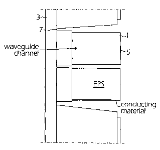
When manufacturing waveguides, for example densely located waveguide channels,
for electromagnetic waves such as microwaves, the channels are produced from
rod-shaped bodies (1) of a material permeable to the waves and non
significantly attenuating the waves. The bodies (1) can for example project
from a base plate (3) and their side surfaces are coated with electrically
conducting material but not their free end surfaces (5). The interior of the
bodies form the waveguiding channels, which have their walls formed from the
layer of electrically conducting material. By giving the rod-shaped bodies
suitable shapes for example an antenna side or half of a waveguide antenna can
be manufactured. The rod-shaped bodies can before applying the electrically
conducting material be coated with one or several layers of non-attenuating
and non-conducting lacquer filling pores and smoothing the surface of the
bodies. Thereby, the layer of electrically conducting material obtains a
smooth transition surface to the material of the bodies giving the channels
good waveguiding characteristics. If the material used in the bodies has a
strong surface porosity, the channels formed from the rod-shaped bodies become
strongly attenuating to the electromagnetic waves. A set of such bodies
located at the sides of each other and having suitable dimensions of the
bodies gives an element working strongly attenuating to the electromagnetic
waves.


French Abstract

Quand on fabrique des guides d'ondes, par exemple, des canaux guide d'ondes regroupés en ensembles de forte densité, pour des ondes électromagnétiques, telles que des micro-ondes, on élabore ces canaux à partir de corps (1) présentant la forme d'une tige et constitués d'un matériau perméable aux ondes et n'exerçant qu'une atténuation limitée sur ces ondes. Ces corps (1) peuvent, par exemple, former une saillie depuis une plaque de base (3) et leurs surfaces latérales sont revêtues par un matériau conducteur électriquement mais pas leurs surfaces d'extrémité libre (5). L'intérieur de ces corps constitue les canaux de guidage d'ondes, dont les parois sont créées à partir de la couche de matériau conducteur électriquement. Les formes appropriées que l'on donne à ces corps permettent de fabriquer par exemple, un côté d'antenne ou la moitié d'une antenne à guide d'ondes. On peut revêtir ces corps en forme de tige, avant l'application du matériau conducteur électriquement, d'une ou de plusieurs couches de laque n'exerçant aucun effet d'atténuation ni de conduction remplissant les pores et lissant la surface des corps. Ceci permet à la couche de matériau conducteur électriquement de posséder une surface de transition lisse par rapport au matériau des corps, ce qui confère aux canaux d'excellentes caractéristiques de guidage d'ondes. Si le matériau utilisé pour ces corps comporte une forte porosité de surface, les canaux créés à partir de ces corps exerceront un effet de forte atténuation par rapport aux ondes électromagnétiques. Un ensemble de ces corps situé côte-à-côte et possédant des dimensions adéquates permet d'obtenir un élément exerçant une forte atténuation par rapport aux ondes électromagnétiques.

Claims

Note: Claims are shown in the official language in which they were submitted.


5

CLAIMS


1. A method of manufacturing a waveguide channel for electromagnetic waves, in
particular microwaves, characterized in that a body is produced from a
material substantially
permeable for the electromagnetic waves and/or not significantly attenuating
the
electromagnetic waves and having a shape corresponding to the shape of the
waveguiding
channels and that exterior surfaces of the body is coated with electrically
conducting material.

2. A method according to claim 1, characterized in that the body is first
coated with at
least one layer of electrically non-conducting lacquer or paint that is
substantially permeable
to and/or is not significantly attenuating to the electromagnetic waves and
that fills pores and
smooths the surfaces of the bodies, and that thereafter the coating with
electrically conducting
material is made.

3. A method according to claim 1, characterized in that to the body is first
applied a
layer of an electrically non-conducting liquid that fills pores and smooths
the surfaces of the
body, and that thereafter the coating with electrically conducting material is
made, the liquid
being selected to prevent the electrically conducting material from
penetrating into the body
and to be evaporated after coating with the electrically conducting material.

4. A method according to claim 1, characterized in that a plurality of bodies
are
produced as a multitude of rod-shaped bodies located at each other.

5. A method according to claim 1, characterized in that a plurality of bodies
are
produced as a plurality of rod-shaped bodies located at each other which
project from a base
plate.

6. A method according to claim 1, characterized in that the body is produced
from an
expanded polymer material, in particular expanded polystyrene.

7. A method according to claim 1, characterized in that the body is produced
from a
polymer material having a surface porosity.

8. A method according to claim 1, characterized in that the layer of
electrically non-
conducting lacquer is applied to the bodies by dipping or an inmould-method.

9. A method according to claim 1, characterized in that waveguiding channels
are
separately produced and are thereafter joined to each other.

10. A method according to claim 1, characterized in that at least two separate
bodies
are produced and coated with electrically conducting material and that the
bodies are
thereafter joined to each other.

11. A method according to claim 1, characterized in that side surfaces and
only one
end surface of the body are coated with the electrically conducting material
to give a
reflection, so that incoming electromagnetic waves first pass into the channel
formed by the
body through the uncoated end surface and then turn and pass out of the same
channel.

12. A method according to claim 1, characterized in that only two opposite
side
surfaces of the body are coated with the electrically conducting material for
obtaining lenses
or filters intended for only a single polarisation of the electromagnetic
waves.


6

13. A waveguide channel for electromagnetic waves, in particular microwaves,
charac
terized by a body of a material substantially permeable for the
electromagnetic waves and/or
not significantly attenuating the electromagnetic waves having a shape
corresponding to the
shape of the waveguiding channels, exterior surfaces of body coated with a
layer of elect
rically conducting material.

14. A method of manufacturing a structure attenuating to electromagnetic
waves, in
particular microwaves, characterized in that a plate-shaped body is produced
from a material
substantially permeable for the electromagnetic waves and/or insignificantly
attenuating for
the electromagnetic waves having a surface porosity including cut-outs or
recesses made in a
first large surface of the body and that the first large surface is coated
with electrically
conducting material for forming an electrically conducting surface layer
having a rough lower
surface at the continuation to the permeable and/or non-attenuating material,
so that for waves
incoming to the body, to a second, opposite large surface of the body, the
rough lower
surface works attenuating.

15. A method according to claim 14, characterized in that in producing the
plate-
shaped body the cut-outs or recesses are given such a shape that therebetween
projecting rods
are formed the dimensions of the cross-sections of which somewhere is larger
than half the
wavelength of the electromagnetic waves in the material having a surface
porosity so that in
addition to the attenuating effect produced by the rough lower surface the
waves are also
prevented because of the cross-sectional dimensions of the channels formed by
the rods into
which they penetrate.

16. A structure for attenuating electromagnetic waves, in particular
microwaves, char-
acterized by a plate-shaped body of a material substantially permeable for the
electromagnetic waves and/or not significantly attenuating the electromagnetic
waves and
having a surface porosity, the body having cut-outs or recesses made in a
first large surface
of the body and the first large surface being coated with an electrically
conducting surface
layer of electrically conducting material, that has a lower surface at the
continuation to the
permeable and/or non-attenuating material, which is rough because of the
electrically
conducting material penetrating into surface pores of the body, so that for
waves incoming to
a second, opposite large surface of the body, the rough lower surface works
attenuating.


Description

Note: Descriptions are shown in the official language in which they were submitted.


CA 02408558 2002-11-05
WO 01/86751 PCT/SE01/00991
1
A METHOD OF FABRICATING WAVEGUIDE CHANNELS
TECHNICAL FIELD
The present application relates to a method of manufacturing waveguide
channels for
microwaves, in particular waveguide channels arranged closely at or at the
sides of each o
s ther, and furthermore a method of manufacturing elements for attenuating
microwaves.
BACKGROUND
In waveguide antennas for receiving and transmitting electromagnetic radiation
having
frequencies in for example the GHz range the largest possible portion of the
surface of the
antennas should consist of open channels that are densely packed, i.e. are
located closely at
o or at the sides of each other. This results in that the walls between the
channels become long
and narrow. Manufacturing such long channels is impossible using the
technology which at
present is available for mass production. Waveguide antennas having such
channels are for
example disclosed in the published International patent application WO
94/11920.
Waveguide channels for microwaves are generally often made as metal tubes
having
,s accurate internal dimensions. Due to the required high accuracy the
manufacture is costly and
such channels therefore have high prices.
SUMMARY OF THE INVENTION
It is an object of the invention to provide a low-cost method of manufacturing
waveguiding channels for electromagnetic waves such as microwaves.
2o It is another object of the invention to provide a simple method of
manufacturing panels
attenuating electromagnetic waves such as microwaves.
Thus, a body can be made from a material permeable for electromagnetic waves
and
thereafter be coated with electrically conducting material such as being
metallized on some of
its surfaces. For a suitable shape of the body and suitably selected
metallized surfaces thereof
zs then the interior of the body forms a waveguiding channel having wall
surfaces constituted by
the interior surfaces of the electrically conducting metal layer. The body can
be given a
suitable geometric shape so that different waveguiding devices can be obtained
such as simple
separate channels, waveguide lenses and filters.
If the material of the body has a surface porosity, suitably the surfaces of
the body are
ao first coated with a surface smoothing or evening material that does not
significantly affect the
propagation of the electromagnetic waves. This material can either be
permanent or made to
evaporate after coating with the electrically conducting material.
The surface porosity can also be employed for manufacturing a structure
attenuating
electromagnetic waves, in particular microwaves. The a plate shaped body can
be produced
35 having cut-outs or recesses made in a first large surface of the body.
Thereafter the first large
surface is coated with electrically conducting material for forming an
electrically conducting
surface layer having a rough lower surface at the continuation to the
permeable or non-
attenuating material having a surface porosity. The interior surface of the
conducting material
obtains such a roughness that it works strongly attenuating to waves incoming
to the second,


CA 02408558 2002-11-05
WO 01/86751 PCT/SE01/00991
2
opposite large surface of the body. The cut-outs or recesses are suitably
given such shapes
that between them projecting rods are formed, the dimensions of the cross-
sections of which
somewhere are larger than half the wavelength of the electromagnetic waves in
the material
having a surface porosity. In addition to the attenuating effect resulting
from the rough lower
s surface the waves are also hindered because of the dimensions of the cross-
sections of the
channels formed in the rods.
BRIEF DESCRIPTION OF THE DRAWINGS
The invention will now be described by way of non limiting embodiments with
reference to the accompanying drawings in which:
,o - Fig. 1 is a perspective view of a portion of a half of a waveguide
antenna,
- Fig. 2a is a cross-sectional view of a portion of a waveguide antenna,
- Fig. 2b is a cross-sectional view corresponding to Fig. 2a in a larger
scale,
- Fig. 3 is a perspective view of a waveguide antenna in which half of an
antenna side is
removed,
15 - Fig. 4 is a perspective view of waveguides placed at the side of each
other having special
cross-sections, and
- Fig. 5 is a view of an attenuating panel.
DETAILED DESCRIPTION
Materials exist which have such a low attenuation of electromagnetic waves
that they
zo can approximately be considered as air in spite of the fact that they in
other respects have
characteristics of solids. An example of such a material is EPS (Expanded
Polystyrene) that
has an attenuation coefficient smaller than 0.1 dB/dm. This material can be
easily used for
manufacturing bodies having very varying shapes. In Fig. 1 is in a perspective
view shown a
portion of a waveguide antenna made from such a material having an
insignificant attenuation
as for electromagnetic radiation, sea also the part cross-sectional view of
Fig. 2a. The
waveguide antenna is formed from rods 1 that project to one side from a for
example flat
base plate 3 keeping the antenna together to form one unit. The rods 1 are on
their side
surfaces coated with an electrically conducting layer, see the description
hereinafter. The end
surfaces 5 of the rods have no such coating but in contrast there is a
conducting coating on
ao the free surface portions 7 of the base plate which are located between the
rods 1. Thereby
the interior of the rods, i.e. the regions inside them, interior of the
electrically conducting
surface layers, waveguiding channels. The rods 1 have furthermore geometric
shapes adapted
to the refracting function of the waveguide antenna so that the waveguiding
channels together
give the desired lens function. The rods can thus be tapering in a direction
away from the
35 base plate 3, as seen in the figures.
When using the above mentioned material EPS and similar expanded polymer
materials
such as expanded polyurethane for manufacturing waveguiding channels according
to the
description above, bodies of the material can be first produced by expansion
caused by a
suitable heating of an adapted amount of non-expanded material placed in a
close mould


CA 02408558 2002-11-05
WO 01/86751 PCT/SE01/00991
3
cavity. Then the produced bodies can be coated with an electrically conducting
paint for
producing the conducting surface layer. The material of bodies produced in
that way is
however at the same time often porous, and if bodies made therefrom are
directly coated with
a conducting paint; pores 9 ~ at the surface of the bodies are filled with the
conducting paint.
s These pores can extend a good distance into the expanded polymer bodies, see
Fig. 2b. A
surface having such pores filled with an electrically conducting material is
rough and
attenuates electromagnetic wave propagating inside the bodies. The result is -
particularly in
the case where the bodies of the material contains pores extending deeply from
the surface -
that the interior of the bodies do not obtain any waveguiding properties for
electromagnetic
o waves and thus do not work as waveguides due to the fact that the interior
of the bodies have
metal walls which are strongly attenuating for electromagnetic waves inside
the bodies.
To avoid such attenuating effects the bodies of the structural material used,
for example
EPS, are first coated with one or several layers of an electrically non-
conducting lacquer that
does not work significantly attenuating for electromagnetic waves and that
both fills the
,s surfaces pores and smooths fine surface of the bodies. Thereafter the
electrically conducting
lacquer is applied and it then forms a completely smooth outer-most layer on
the bodies
having in particular a smooth interior surface where this lacquer continues
into the next
underlying layer of non attenuating lacquer. The layer of electrically non-
conducting lacquer
can be applied to the bodies by dipping or immersing or by inmould-methods.
o Alternatively the bodies can be first coated with an electrically non
conducting liquid
that also both fills surface pores of the bodies and smooths the surface of
the bodies. The
liquid can be selected so that it prevents the electrically conducting lacquer
from penetrating
into the bodies and so that it is evaporated or evaporates after applying the
electrically
conducting lacquer. Such a liquid can include a liquid, for example water,
that is completely
a5 non-miscible with the electrically conducting lacquer.
To mass manufacture waveguiding structures for for example antenna function
often
several moulds are required, for example one mould for one side and another
one for the
opposite side. In Fig. 3 a waveguide antenna is shown in which half of an
antenna side. is
removed. Using this manufacturing method it is possible to make channels
having adjacent
ao sides in common and a more narrow interior portion. In such a case, as has
been described
above with reference to Figs. 1 and 2, the sides of the rods 1, which then
correspond to
portions of waveguide channels, and the common surfaces 7 between two rods are
coated
with conducting material but not the surface 5, at which two halves are to be
joined to each
other. Thereafter opposite surface of the antenna sides are joined to each
other and continuous
as channels having optimized entrance and exit sides are obtained.
Devices having different kinds of waveguiding channels can be manufactured. In
Fig. 4
for example waveguides are shown that are obtained from rods located at the
sides of each
other and having T-shaped cross-sections. The rods 1 generally have different
shapes
depending on the intended application. Thus they can have substantially square
cross-sections,


CA 02408558 2002-11-05
WO 01/86751 PCT/SE01/00991
4
such as for waveguide channels for general use, or rectangular cross-sections,
such as for
waveguide lenses, filters and plan/circular-rotating arrays intended for only
one of the
polarisations of an electromagnetic wave.
Reflecting waveguides, not shown, can be manufactured by first producing
suitable rod
s shaped bodies according to the description above and that then one of the
end surfaces of the
bodies are coated with electrically conducting material in addition to the
side surfaces. This
gives a reflection, so that an incoming electromagnetic wave first enters the
channels formed
by the bodies from the uncoated ends of the rods and then turns and exits the
same channels.
If suitable rod-shaped bodies are first produced according to the description
above and
o then only two opposite side surfaces of the bodies are coated with
electrically conducting
surface layers, lenses or filters formed from parallel plates can be obtained
which are
intended for electromagnetic waves having a single polarisation.
The rods should generally have cross-sectional dimensions larger than half the
largest
wavelength for which their waveguiding functions are to be utilized for
amplifying or
15 filtering.
Simple waveguide channels, not shown, can be manufactured in the similar way.
A
simple straight body having for example a uniform rectangular cross-section is
first produced.
The body is bent to the desired shape and is then coated with one or several
layers of
electrically non-conducting lacquers, for example of an epoxy polymer, and
finally with a
zo layer of electrically conducting material. The coating with lacquers and in
particular with a
polymer material results in that the body will permanently maintain its shape.
The property of attenuating electromagnetic waves of bodies of the mentioned
materials
directly coated with an electrically conducting lacquer can be used for
manufacturing
attenuating surface panels. An example of such a panel is shown in Fig. 5 and
includes a
z5 plurality of comically shaped or pyramidal recesses located at the sides of
each other and
formed in one of the large surfaces of an otherwise flat body. The recesses
are thus directly
coated with electrically conducting paint. The panel works, for a suitable
shape of the
recesses and provided that the lacquer has well penetrated into the surface
pores of the panel,
attenuating to electromagnetic waves which are incident to the opposite large
surface of the
ao panel that- can be substantially flat and is not coated with an
electrically conducting layer. If a
closed space is lagged with such panels, the flat surfaces of the panels
directed to the interior
of the space, a space is obtained in which possible electromagnetic waves are
efficiently
attenuated. The portions of the recesses located between the panels that
correspond to the
waveguide channels according to the description above should generally
somewhere, for
35 example at their entrances or at their central portions, have cross-
sectional dimensions larger
than half the largest wavelength for which their attenuating function is to be
used.

Representative Drawing
A single figure which represents the drawing illustrating the invention.
Administrative Status

For a clearer understanding of the status of the application/patent presented on this page, the site Disclaimer , as well as the definitions for Patent , Administrative Status , Maintenance Fee  and Payment History  should be consulted.

Administrative Status

Title Date
Forecasted Issue Date 2011-01-04
(86) PCT Filing Date 2001-05-07
(87) PCT Publication Date 2001-11-15
(85) National Entry 2002-11-05
Examination Requested 2006-04-20
(45) Issued 2011-01-04
Deemed Expired 2014-05-07

Abandonment History

Abandonment Date Reason Reinstatement Date
2008-05-07 FAILURE TO PAY APPLICATION MAINTENANCE FEE 2008-07-21

Payment History

Fee Type Anniversary Year Due Date Amount Paid Paid Date
Application Fee $150.00 2002-11-05
Maintenance Fee - Application - New Act 2 2003-05-07 $50.00 2003-04-29
Maintenance Fee - Application - New Act 3 2004-05-07 $50.00 2004-04-19
Maintenance Fee - Application - New Act 4 2005-05-09 $50.00 2005-04-15
Maintenance Fee - Application - New Act 5 2006-05-08 $100.00 2006-04-13
Request for Examination $400.00 2006-04-20
Back Payment of Fees $400.00 2006-04-20
Maintenance Fee - Application - New Act 6 2007-05-07 $100.00 2007-05-01
Reinstatement: Failure to Pay Application Maintenance Fees $200.00 2008-07-21
Maintenance Fee - Application - New Act 7 2008-05-07 $200.00 2008-07-21
Maintenance Fee - Application - New Act 8 2009-05-07 $200.00 2009-05-07
Maintenance Fee - Application - New Act 9 2010-05-07 $200.00 2010-04-14
Final Fee $300.00 2010-10-21
Maintenance Fee - Patent - New Act 10 2011-05-09 $250.00 2011-04-18
Maintenance Fee - Patent - New Act 11 2012-05-07 $250.00 2012-04-17
Owners on Record

Note: Records showing the ownership history in alphabetical order.

Current Owners on Record
PETERSSON, STIG ANDERS
Past Owners on Record
None
Past Owners that do not appear in the "Owners on Record" listing will appear in other documentation within the application.
Documents

To view selected files, please enter reCAPTCHA code :


To view images, click a link in the Document Description column. To download the documents, select one or more checkboxes in the first column and then click the "Download Selected in PDF format (Zip Archive)" or the "Download Selected as Single PDF" button.

List of published and non-published patent-specific documents on the CPD .

If you have any difficulty accessing content, you can call the Client Service Centre at 1-866-997-1936 or send them an e-mail at CIPO Client Service Centre.


Document
Description 
Date
(yyyy-mm-dd) 
Number of pages   Size of Image (KB) 
Abstract 2002-11-05 1 64
Claims 2002-11-05 2 141
Drawings 2002-11-05 5 112
Description 2002-11-05 4 321
Representative Drawing 2003-02-10 1 5
Cover Page 2003-02-11 1 49
Claims 2009-11-27 3 101
Claims 2009-04-02 5 180
Cover Page 2010-12-09 2 55
Fees 2008-05-06 1 43
PCT 2002-11-05 3 109
Assignment 2002-11-05 2 71
PCT 2002-11-06 4 227
Fees 2003-04-29 1 29
Fees 2004-04-19 1 31
Fees 2005-04-15 1 29
Fees 2006-04-13 1 40
Prosecution-Amendment 2006-04-20 2 42
Fees 2007-05-01 1 42
Correspondence 2008-05-30 1 30
Prosecution-Amendment 2008-10-14 3 86
Fees 2008-07-21 2 49
Prosecution-Amendment 2009-04-02 14 535
Prosecution-Amendment 2009-06-03 2 88
Fees 2009-05-07 1 44
Prosecution-Amendment 2009-11-27 6 205
Fees 2010-04-14 1 40
Correspondence 2010-10-21 2 48