Note: Descriptions are shown in the official language in which they were submitted.
CA 02408597 2002-11-06
WO 01/86815 PCT/USO1/14992
1
METHOD AND APPARATUS FOR REDUCING PLL LOCK
TIME
BACKGROUND OF THE INVENTION
I. Field of the Invention
The present invention relates to Phase Locked Loops (PLL's). More
particularly, the present invention relates to a novel and improved method and
l0 apparatus for reducing the time required to obtain phase lock in a PLL that
is
activated following operation in standby mode.
II. Description of the Related Art
l5 Accurate frequency sources are vital to the operation of numerous
electronic systems and devices. Frequency sources are used as timing sources
within electronic devices and are also used to tune electronic devices to
desired
communication channels.
Many types of accurate frequency sources are available. The specific
20 type of frequency source implemented within a particular application is
determined according to the design constraints of the particular application.
Atomic clocks exhibit extreme levels of frequency accuracy, however, their
size,
cost, and absence of tuning range greatly limit their actual application
within
an electronic system. Similarly, accurate frequency sources can be designed
25 utilizing the piezoelectric effect of quartz crystals. The small size and
relative
accuracy of quartz crystal based frequency sources make them popular for
most consumer based electronic devices. However, a frequency source based
upon the fundamental frequency of a quartz crystal is limited by the minimal
frequency tuning range and limitations on the fundamental frequency of a
30 quartz crystal.
Indirect frequency synthesis is used to overcome the problems of the
lack of frequency tuning and limited center frequency associated with
fundamental quartz crystal frequency sources. Indirect frequency synthesis
utilizes a Phase Locked Loop (PLL) to generate a frequency source that is a
35 multiple of a reference frequency. Specific implementations of indirect
frequency synthesis often use a quartz crystal oscillator as the reference
frequency.
CA 02408597 2002-11-06
WO 01/86815 PCT/USO1/14992
2
A frequency source implemented using indirect frequency synthesis is
commonly known as a frequency synthesizer. A common implementation of a
frequency synthesizer is shown in FIG. 1. A quartz crystal 20 is coupled to an
oscillator 30 to generate a reference frequency. A reference divider 32 is
coupled to the output of the oscillator 30 to scale the reference frequency. A
Voltage Controlled Oscillator (VCO) 60 operates to provide the desired output
of the frequency synthesizer 10. The output of the VCO 60 is also coupled to
an
output frequency divider 62 that generates a scaled output of the VCO 60. The
output of the reference divider 32 is coupled to a first input of a phase
detector
40. The output of the output frequency divider 62 is coupled to a second input
of the phase detector 40. The phase detector 40 compares the scaled output
from the output frequency divider 62 to the scaled output from the reference
divider 32. The phase detector 40 output is a control signal based upon the
comparison of the input signals. The phase detector 40 output is coupled to a
loop filter 50 that limits the frequency component of the phase detector 40
output. The output of the loop filter 50 is coupled to a control input on the
VCO 60. The signal on the control input of the VCO 60 operates to tune the
VCO 60 output frequency. The frequency synthesizer 10 is thus a phase locked
loop wherein the loop operates to maintain phase lock between the scaled
reference frequency and the scaled output frequency. The common
architecture of a frequency synthesizer 10 allows for a number of the
functional
blocks to be combined within a single Integrated Circuit (IC). A typical
frequency synthesizer IC integrates the oscillator 30, reference divider 32,
output frequency divider 62, and phase detector 40. The user is only required
to provide the additional elements consisting of a crystal 20 for the
oscillator 30,
a VCO 60, and a loop filter 50 to complete the frequency synthesizer 10.
The operation of a Phase Locked Loop (PLL) is characterized by a
number of parameters. These characteristics include the pull in time and pull
in range. The pull in range is defined as the range of frequencies over which
the PLL will acquire and lock the VCO output to the reference frequency. The
pull in time represents the time required for the pull in process. Both the
pull
in range and pull in time are affected by the type of phase detector used in
the
PLL as well as the order of the loop filter.
The time the PLL takes to acquire and lock a VCO output signal is
important in many applications. PLL lock time design constraints are
determined by the specific application. Frequency synthesizers utilizing PLL's
are used within portable communication devices to generate Local Oscillator
(LO) signals. LO signals are used to tune receivers and transmitters to
specific
CA 02408597 2002-11-06
WO 01/86815 PCT/USO1/14992
3
channels. Typically, in a receiver the LO is used to downconvert the received
RF signal to a baseband signal. Conversely, in a transmitter a LO is used to
upconvert baseband signals to designated RF channels. Frequency synthesizers
used for the generation of LO signals are fotu~d in devices such as two-way
radios, stereo receivers, televisions, and wireless phones. However, one of
ordinary skill in the art will recognize that frequency synthesizers are not
limited to the generation of LO signals. Frequency synthesizers are capable of
satisfying the requirements of the majority of frequency source applications.
Frequency synthesizer power consumption is an important design
concern when the frequency synthesizer is used in a portable electronic
device.
The battery life on a portable electronic device decreases in proportion to
increases in power consumption. Therefore, minimization of power
consumption is highly desirable in electronic circuits used in portable
electronic
devices.
Portions of a wireless phone may be powered down under certain
conditions in order to conserve battery power and extend battery life. In a
wireless phone operating in a Code Division Multiple Access (CDMA)
communication system, such as the one described in Telecommunications
Industry Association (TIA)/Electronics Industries Association (EIA) 95-B
MOBILE STATION-BASE STATION COMPATIBILITY STANDARD FOR
DUAL-MODE SPREAD SPECTRUM SYSTEMS, the phone may power down
specific circuits under a variety of conditions. The system described by
TIA/EIA 95-B allows the phone to operate at a reduced data rate during a
phone call under certain conditions. When the phone is operating in the
reduced data rate mode the phone's transmitter transmits bursts of data
packets. To conserve power, portions of the phone's transmit chain are
powered down during the time period in which the phone is not required to
transmit any data.
Additional power savings are achieved by powering down portions of
the phone during the time the phone is in the idle state where a call is not
in
progress. A CDMA phone operating in a TIA/EIA 95-B system performs a
number of tasks while in the idle state. These tasks include performing
registration procedures and idle handoff procedures. Additional tasks include
receiving overhead messages, configuration messages, page messages, mobile
station directed orders, data burst messages and acknowledgements for access
channel messages. The phone is not continually active in the idle state. To
take
advantage of the limited phone activity in the idle state, portions of the
phone
can be powered down during periods within the idle state to further reduce
CA 02408597 2002-11-06
WO 01/86815 PCT/USO1/14992
power consumption and increase battery life. The phone can be placed in a
standby or sleep mode during the idle state when no phone activity is
required.
Only critical portions of the phone remain powered up during sleep mode. All
remaining non-critical portions of the phone are powered down to minimize
phone power consumption. The frequency synthesizer used to generate the LO
signals is one of the non-critical circuits powered down during the sleep
mode.
However, the phone is periodically required to wake up and service the
required idle state tasks. When the phone wakes up it is required to
synchronize its timing with the system before it can transmit or receive
communications. The time the phone uses to resynchronize with the system
must be minimized in order to maximize the power savings gained by placing
the phone in the sleep mode. The time required by the frequency synthesizer to
tune and lock to the assigned frequency represent part of the phone
synchronization time. Therefore, it is advantageous to minimize the time the
frequency synthesizer uses to tune and lock to the desired frequency.
Standard methods of reducing the lock time of a PLL include increasing
the VCO gain, increasing the bandwidth of the loop filter, and decreasing the
damping factor of the loop filter. However, these lock time reduction methods
are not available to the designer interested in reducing the PLL lock time for
a
frequency synthesizer that is switched from a sleep state to an idle mode in a
wireless phone. This is because the performance of the frequency synthesizer
in the locked state determines the majority of the parameters of the PLL. The
values of VCO gain, loop filter bandwidth, and loop filter damping factor are
limited by the design constraints imposed on the locked output of the
frequency synthesizer. What is needed is a manner of improving the frequency
synthesizer PLL lock time without degrading the performance of the frequency
synthesizer output when the loop is locked.
SUMMARY OF THE INVENTION
The present invention is a novel and improved method and apparatus
for decreasing the time required for a frequency synthesizer to lock after
waking up from a sleep or standby mode. When the frequency synthesizer is
placed in the sleep or standby mode the voltage on the VCO tuning line is
maintained. The portions of the frequency synthesizer required to maintain
phase lock are powered down during sleep mode to conserve power. The
powered down circuits include the reference divider, phase detector, and
CA 02408597 2002-11-06
WO 01/86815 PCT/USO1/14992
output frequency divider. The voltage on the VCO tuning line is maintained at
the voltage value that was on the VCO tuning line just prior to the frequency
synthesizer being placed in the sleep mode.
In a frequency synthesizer Integrated Circuit (IC) the voltage at the VCO
5 tune pin is maintained when the IC is placed in sleep mode. The IC samples
the voltage value of the VCO control line just prior placing the IC in the
sleep
mode. The sampled value is maintained at the VCO tune pin of the frequency
synthesizer IC.
BRIEF DESCRIPTION OF THE DRAWINGS
The features, objects, and advantages of the present invention will
become more apparent from the detailed description set forth below when
taken in conjunction with the drawings in which like reference characters
identify correspondingly throughout and wherein:
FIG.1 is a block diagram of a frequency synthesizer;
FIG. 2 is a block diagram of a frequency synthesizer in a wireless phone;
FIG. 3 is a block diagram of a frequency synthesizer that maintains the
VCO control voltage in low power modes; and
FIG. 4 is a block diagram of a circuit used to maintain the VCO control
voltage.
DETAILED DESCRIPTION OF THE PREFERRED
EMBODIMENTS
As stated above, the wireless phone environment presents one
application in which a frequency synthesizer is eommonly used. FIG. 2
presents a block diagram of one possible configuration of a wireless phone
showing an application of a frequency synthesizer.
The wireless phone 200 is configured to operate over distinctly defined
RF channels. One band of RF frequencies is designated the transmit band and a
different distinct band of RF frequencies is designated the receive band. The
two bands are typically closely spaced but do not overlap. Receive signals are
coupled to the wireless phone 200 through the antenna 210. The received
signals are coupled from the antenna 210 to a duplexer 220. The duplexer 220
is used to couple receive signals from the antenna 210 to the receiver 230
while
simultaneously attenuating energy in the transmit band. Receive signals
output from the duplexer 220 are coupled to a receiver 230. The receiver 230
CA 02408597 2002-11-06
WO 01/86815 PCT/USO1/14992
6
filters, amplifies, downconverts, and processes the received signal. The
receiver 230 incorporates user interfaces that enable it to present the
received
information to the user. The user interface may include an earpiece speaker to
provide audio output to the user as well as a display to provide textual or
graphical output to the user.
The transmit path of a wireless phone 200 includes a baseband 250
circuit that provides the interface between the phone 200 and the user. The
user interface may include a keypad, a touch sensitive screen, and a
microphone. The baseband circuit 250 collects and processes the user input.
The type of processing includes conditioning the input and modulating the
input in the modulation format specified by the phone system. The input
signal conditioning may consist of filtering as well as digitizing.
The processed baseband signal is then upconverted to an Intermediate
Frequency (IF). Upconversion of the baseband signal is performed using a first
mixer 252 in conjunction with a first Local Oscillator (LO) 254. The first LO
254
is typically a fixed LO such that the IF is constant within a predetermined
narrow band. A fixed first LO 254 minimizes the complexity required in the IF
processing section 260. The IF processing circuit 260 filters and amplifies
the
upconverted baseband signal. The IF section 260 may include an Automatic
Gain Control (AGC) section to ensure that subsequent amplifiers are not
compressed. The output of the IF section 260 is coupled to a second mixer 262
that uses the output of a frequency synthesizer 264 to upconvert the IF signal
to
an RF signal. The frequency synthesizer 264 is capable of tuning in discrete
steps over a frequency band to provide upconversion of the IF signal to a
specified RF channel.
The upconverted output of the second mixer 262 is coupled to an RF
section 266 where the RF signal is filtered and amplified. The RF section 266
filters out the unwanted mixer products as well as filtering out spurious
frequency components that degrade the quality of the RF signal. The output of
the RF section 266 is coupled to an amplifier 270 that provides the final gain
stage for the transmit signal. The output of the amplifier 270 is coupled to
an
isolator 280. The isolator 280 is used to prevent signal reflections and
energy
coupled in the transmit frequency band from reaching the transmit circuits of
the phone 200. The output of the isolator 280 is coupled to the duplexer 220
which couples the transmit RF signal to the antenna 210.
The use of a common antenna 210 for both the transmit and receive
signals is accomplished by using the duplexer 220 to couple the signals to and
from the antenna 210. In the receive path the duplexer 220 couples the signal
CA 02408597 2002-11-06
WO 01/86815 PCT/USO1/14992
received at the antenna 210 to the receiver 230 while rejecting signals in the
transmit frequency band. The signals in the transmit frequency band are
rejected in the duplexer 220 path to the receiver to eliminate the possibility
of
saturating the receiver 230 with transmit power.
The wireless phone 200 powers down a number of circuits when it is
placed in the sleep mode to conserve battery power. Portions of the receiver
230 are powered down as well as significant portions of the transmitter. The
amp 270, RF section 266, IF section 260, and frequency synthesizer 264 are
powered down when the wireless phone 200 is in sleep mode.
However, it is not advantageous to completely power down all circuits
because the wireless phone 200 needs to periodically wake up and service
overhead tasks required in the communication system. A minimal number of
circuits remain powered up to minimize the wake up time required by the
wireless phone 200. Maximizing the sleep time maximizes the amount of
power that is conserved. Minimizing the wake up time of the phone maximizes
the phone sleep time.
One method of minimizing the wake up time of the phone is to
minimize the lock time associated with the frequency synthesizer. An
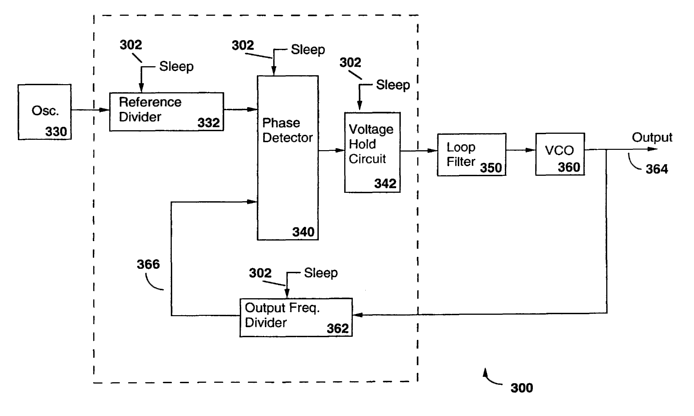
exemplary embodiment that accomplishes this is shown in FIG. 3. FIG. 3
depicts a block diagram of a frequency synthesizer 300 having active and sleep
modes. When the frequency synthesizer 300 is placed in the sleep mode the
voltage value on the VCO control line 352 is maintained. The frequency
synthesizer 300 of the exemplary embodiment operates as a conventional
frequency synthesizer when the frequency synthesizer 300 is operated in the
active mode.
The reference oscillator 330 produces a stable reference signal. The
output of the reference oscillator 330 is coupled to the input of a reference
divider 332. The reference divider 332 scales the frequency of the reference
oscillator 330. The output of the reference divider 332 is coupled to a first
input
on the phase detector 340. The reference divider 332 is controlled by a sleep
signal 302 which commands the reference divider 332 to power down when the
phone is in the sleep mode. When the reference divider 332 is powered down
in the sleep mode the value of the divider ratio may be lost. If this is the
case
the divider ratio will need to be reprogrammed when the reference divider 332
is commanded to wake up. Alternatively, the divider ratio of the reference
divider 332 may be hard wired or stored in nonvolatile memory such that loss
of power does not result in its loss. The divider xatio of the reference
divider
332 may also be stored in a portion of memory that is not powered down when
CA 02408597 2002-11-06
WO 01/86815 PCT/USO1/14992
the reference divider 332 is commanded to go into the sleep mode. The choice
as to which configuration is most advantageous will depend on the specific
frequency synthesizer 300 application.
Reference dividers 332 are typically used in most frequency synthesizers
300 to allow the use of a higher frequency reference oscillator 330 while
maintaining a lower frequency at the input to the phase detector 340. A higher
frequency reference oscillator 330 permits a more reasonably sized crystal
oscillator. However, a lower frequency is desirable at the phase detector 340
input because the frequency of the phase detector 340 determines the tuning
step size of the frequency synthesizer 300. The reference divider's 332
inclusion
in the frequency synthesizer 300 is not mandatory and one of ordinary skill in
the art will recognize that the frequency synthesizer 300 can be implemented
without a reference divider 332.
The VCO 360 generates the output signal 364 of the frequency
synthesizer 300. The VCO 360 output frequency is determined by the signal
applied at the control input of the VCO 360. The VCO 360 output is also
coupled to an output frequency divider 362. The output frequency divider 362
scales the frequency of the VCO 360 to the frequency of the phase detector
340.
The output frequency divider 362 is advantageous when the frequency
synthesizer 300 is required to tune over multiple channels. The frequency
synthesizer 300 can also be tuned by varying the reference divider 332 or the
reference oscillator 330, however, the most common method is the utilization
of
the output frequency divider 362.
The output frequency divider 362 is controlled by a sleep signal 302
which commands the output frequency divider 362 to power down when the
phone is in the sleep mode. The value of the output divider ratio, analogous
to
the reference divider ratio, may be lost when the output frequency divider 362
is commanded to go into the sleep mode. However, like the reference divider
ratio value, the output frequency divider ratio value can be saved in
nonvolatile memory or can be saved in a memory location that is not powered
down when the output frequency divider is commanded to go into the sleep
mode.
The scaled frequency output 366 of the output frequency divider 362 is
coupled to a second input on the phase detector 340. The phase detector 340
compares the two input signals and outputs a signal based on the phase error
between the two input signals. The phase detector 340 is controlled by a sleep
signal 302 which commands the phase detector 340 to power down when the
phone is in the sleep mode.
CA 02408597 2002-11-06
WO 01/86815 PCT/USO1/14992
9
The output of the phase detector 340 is coupled to the input of a voltage
hold circuit 342 that is designed to maintain the VCO 360 control voltage
signal
when the frequency synthesizer is placed in the sleep mode. The actual
implementation of the voltage hold circuit 342 depends on the type of phase
detector 340 used in the loop. The voltage hold circuit 342 can be a sample
and
hold circuit where the output voltage of the phase detector is sampled
continuously and held when the sleep signal 302 indicates the frequency
synthesizer 300 is placed in the sleep mode. The sleep signal 302 commanding
the voltage hold circuit 342 does not cause it to power down in the sleep
mode.
Instead, the sleep signal 302 commands the voltage hold circuit 342 to change
from sampling the voltage on the control line, when the sleep signal 302
indicates an active mode, to maintaining the voltage on the control line when
the sleep signal 302 indicates sleep mode.
The output of the voltage hold circuit 342 is coupled to the input of a
loop filter 350. The loop filter acts to limit the bandwidth of the VCO 360
control signal. The loop filter 350 is commonly implemented as a passive
filter
and therefore requires no external power source. However, the loop filter 350
can be implemented as an active filter. The output of the loop filter 350 is
coupled to the control input of the VCO 360. As stated above, the output
frequency of the VCO 360 is determined by the signal applied at the control
input.
When the frequency synthesizer 300 is operating in the active mode all
of the elements in the synthesizer are active and the voltage hold circuit 342
allows the output from the phase detector 340 to proceed unchanged to the
loop filter 350. The loop operates to lock the VCO 360 output to the reference
frequency when the frequency synthesizer 300 is in the active mode. When the
frequency synthesizer is commanded to the sleep mode those elements that
utilize the sleep signal 302 as a power control signal are powered down. The
voltage hold circuit 342 utilizes the sleep signal 302 to maintain the voltage
on
the VCO 360 control line 352 at the value just prior to the application of the
sleep signal 302.
When the frequency synthesizer 300 is commanded to return to the
active mode from the sleep mode the VCO 360 initially operates at a frequency
much closer to the frequency desired when the loop is locked. Therefore, the
initial frequency error in the loop is smaller than if the VCO control voltage
were not controlled during the sleep mode. The loop is able to reduce the time
it takes to lock the VCO 360 to the reference frequency 330 because of the
smaller initial frequency error. The reduction in lock time serves to reduce
the
CA 02408597 2002-11-06
WO 01/86815 PCT/USO1/14992
time the phone requires to service any idle state overhead tasks. This allows
the phone to maximize the sleep time thereby maximizing battery life.
An exemplary configuration of a voltage hold circuit 342 is shown in
FIG. 4. The voltage hold circuit 342 incorporates an input 402 for cotlpling
5 signals to the circuit. Signals from the phase detector 340 output couple to
the
voltage hold circuit 342 input 402. The input 402 is the non-inverting input
to a
first amplifier 404 configured as a unity gain buffer. The output of the first
amplifier 404 is coupled to the input of a switeh 410. The switch 410 is shown
as a FET in FIG. 410 but any type of switch with suitable switching
10 characteristics can be used in the application. The output of the switch
410 is
coupled to the non-inverting input of a second amplifier 420 configured as a
unity gain buffer. Additionally, a capacitor 414 is coupled to the non-
inverting
input of the second amplifier 420. A first terminal of the capacitor 414 is
coupled to the non-inverting input of the second amplifier 420, while the
second terminal of the capacitor 414 is coupled to ground. The output of the
second amplifier 420 serves as the output 422 of the voltage hold circuit 342.
A
control line, labeled HHHoId Control 412 in FIG. 4, is used to control the
position of the switch 410. The Hold Control 412 line is controlled by the
sleep
signal 302 when the circuit of FIG. 4 is used as the voltage hold circuit 342
of
. FIG. 3.
The voltage hold circuit 342 functions in either a transparent mode or a
hold mode. The voltage hold circuit 342 operates in the transparent mode, also
known as a sample mode, when the Hold Control 412 line commands the
switch 410 to the closed circuit position. The output of the first amplifier
404 is
identically the input to the voltage hold circuit 342. The output of the first
amplifier 404 is couple to the non-inverting input of the second amplifier 420
when the switch 410 is in the closed position. The capacitor 414 couple to the
same non-inverting input to the second amplifier 420 tracks the voltage output
of the first amplifier 404. The output of the second amplifier 420, which
serves
as the output 422 of the voltage hold circuit 342, tracks the voltage on the
capacitor 414.
The voltage hold circuit 342 operates in the hold mode when the Hold
Control 412 line commands the switch 410 to the open circuit position. The
output of the first amplifier 404 is no longer coupled to the input of the
second
amplifier 420 when the switch 410 is in the open circuit position. Instead,
the
capacitor 414 serves as the only element that is coupled to the input of the
second amplifier 420. However, the capacitor 414 stores the voltage that was
across its terminals when the switch 410 was in the closed position. Thus,
when
CA 02408597 2002-11-06
WO 01/86815 PCT/USO1/14992
11
the switch 410 is in the open circuit position, the second amplifier 420
outputs
the voltage stored in the capacitor 414. The voltage stored in the capacitor
414
represents the last voltage value output from the first amplifier 404 prior to
open circuiting the switch 410. The output of the second amplifier 420 is
constant in the hold mode since the first amplifier 404 no longer drives the
voltage level across the capacitor 414.
The output of the second amplifier 420, which is the output of the
voltage hold circuit 342, is coupled to the loop filter 350. The loop filter
350
serves to couple the VCO control voltage to the VCO 360. Therefore, it can be
seen that the circuit of FIG. 4 can be used to allow continuous control over
the
VCO control voltage or can be used to maintain the VCO eontrol voltage at a
given level.
The previous description of the preferred embodiments is provided to
enable any person skilled in the art to make or use the present invention. The
various modifications to these embodiments will be readily apparent to those
skilled in the art, and the generic principles defined herein may be applied
to
other embodiments without the use of the inventive faculty. Thus, the present
invention is not intended to be limited to the embodiments shown herein but is
to be accorded the widest scope consistent with the principles and novel
features disclosed herein.
I CLAIM: