Note: Descriptions are shown in the official language in which they were submitted.
CA 02408674 2002-10-16
OUTPUT POWER MONITORING IN AN OPTICAL PREAMPLIFIER
TEC",HNICAL FIELD
The present invention relates to optically amplified receivers and more
particularly,
to output power monitoring in an optical preamplifier in front of a high speed
optical-to-
electrical (O-E) converter to supply an optical signal of substantially
constant output
power.
BAC:',KGROUND INFORMATION
In optical transmission systems, and particularly long-haul transmission
systems,
optical amplifiers are used to amplify optical signals that have become
attenuated and
degraded during transmission. Communication receivers used in optical
transmission
systems often utilize a.n optical preamplifier 10, as shown in FIG. 1, to
amplify an optical
signal before converting the optical signal to the electrical domain. The
optical
preamplifier 10 usually works in a constant output power mode using an optical
Automatic
Power Control (APC) loop 12 to supply an optical .signal of substantially
constant power to
an optical-to-electrical (O-E) canverter 16. Tlae 0-E converter I G
demodulates the
intensity modulated signal and cony erts it to the electrical domain. In a
conventional O-E
converter 16, a photodiode bias voltage 17 is applied to the O-E converter 16
for proper
operation.
An optical preamplifier 10 typically includes an optical gain medium 18, such
as a
rare earth doped fiber, a pump laser 20 for pumping the optical gain medium
18, and
control circuitry 22 for controlling the pump laser 20. In general, the APC
loop 12 works
by detecting the optical power at the output of the optical preamplifier 10
and by providing
a feedback signal. The feedback signal is processed and adjusts the gain of
the gain
medium 18 accordingly to provide substantially constant output power. In
current optical
;preamplifiers, the feedback signal is provided to the control circuitry 22
and the gain
adjustment is generally accomplished by driving the laser 20, which pumps the
optical
gain medium 18 to provide more or less gain.
CA 02408674 2002-10-16
7
In current optical preamplifiers with output power monitoring capability, the
optical power monitor is provided by using an optical tap coupler 26
(generally a separate
optical component) to tap off a pardon of the optical output signal and send
it to a
monitoring photodiode 28. The extra parts (e.g., the tap coupler 26 and
monitoring
photodiode 28) necessary in this existing approach to optical preamplifier
output
monitoring result in extra cost, space, manufacturing effort (splicing, etc.),
and losses in
signal power (e.g., extra splice and tap insertion loss}. Moreover, this
existing approach
stabilizes power at the input of the monitoring photodiode 28 while additional
losses in
power occur between the optical tap 26 and the U-E converter 16, such as
splice and/or
connector interface losses and coupling losses duo to the component aging
(e.g., between
fiber to active surface of the photodetector of the O-E converter 16). Because
these
additional losses are outside of the ~'-1fC loop 12, they are not compensated.
Accordingly, there is a need to implement output power monitoring in an
optical
preamplifier without the use of an output optical tap and monitoring
photodiode. There is
1 S also a need for topless optical output power monitoring in which interface
losses caused by
the tap are eliminated and additional interface and coupling losses are
compensated.
5LJMM.4RY
In accordance with one aspect of the present invention, a method is used for
topless
output power monitoring in an optical preamplifier including an optical-to-
electrical (O-E)
converter for demodulating and converting an intensity-modulated optical
signal into an
electrical output signal. According to the method, a DC bias current of the O-
E converter
is monitored while the O-E converter demodulates and converts the intensity-
modulated
optical signal. The DC,' bias current is directly related to average optical
power incident on
the O-E converter. A feedback signal proportional to the DC bias current is
produced and
used to adjust the optical preamplifier to provide a substantially constant
output power to
'the O-E converter.
In accordance with another aspect of the present invention, a method is used
to
convert an intensity-modulated optical input signal into an electrical output
signal.
CA 02408674 2002-10-16
According to this method, the intensity-modulated optical input signal is
amplified to
produce an amplified intensity-modulated optical signal. The amplified
intensity-
modulated optical signal is demodulated and canverted into the electrical
output signal
using an optical-to-electrical (O-E) converter. The method further comprises
monitoring a
DC bias current of the O-E converter used to demodulate and convert the
intensity-
modulated optical signal and producing a feedback signal proportional to the
DC bias
current. The power of the amplified intensity-modulated optical signal is
adjusted based
on the feedback signal.
According to a further aspect of the present invention, an optical
preamplifier
comprises an optical gain medium for receiving an intensity-modulated optical
input signal
and producing an amplified intensity-modulated optical signal. An optical-to-
electrical
(O-E) converter demodulates and converts the amplified intensity-modulated
optical signal
into an electrical output signal. .A pump laser pumps the optical gain medium
and pump
bias control circuitry controls the pump laser. The optical preamplifier
further comprises a
current monitor for monitoring a D(~ bias current of the O-E converter and for
producing a
feedback signal proportional to the DC bias curr~:.nt. The feedback signal is
provided to
the pump bias control circuitry for adjusting the gain of the optical gain
medium.
In accordance with yet another aspect of the present invention, an optical
communications receiver comprises an optical preamplifier for receiving an
intensity-
modulated optical input signal and producing ary amplified intensity-modulated
optical
signal. An optical-to-electrical (O-E) converter demodulates and converts the
amplified
intensity-modulated optical signal into an electrical output signal. A current
monitor
monitors a DC bias current of the O-E converter and produces a feedback signal
proportional to the DC bias current. The feedback signal is provided to the
optical
preamplifier for adjusting the gain of the optical preamplifier such that the
amplified
intensity-modulated optical signal has substantially constant output power.
CA 02408674 2002-10-16
t1.
BRIEF DESCRIPTION OF THE DRAWINGS
These and other features and advantages of the present invention will be
better
understood by reading the following detailed description, taken together with
the drawings
wherein:
FIG. 1 is a schematic block diagram of the front end of an optical
communications
receiver, according to the prior art, with an optical preamplifier
incorporating optical
automatic power control (APC);
FIG. 2 is a schematic block diagram of a system for converting optical signals
to
electrical signals using the automatic power control with tapless output
monitoring, according
to one embodiment of the present invention;
FIG. 3 is a schematic block diagram of an optical preamplifier with integrated
automatic power control with tapless output monitoring, according to another
embodiment of
the present invention;
FIG. 4 is a schematic diagram of a circuit implementation of the optical
preamplifier,
according to a fiirther embodiment of' the present invention; and
FIG. 5 is a schematic diagram of a circuit implementation of the current
monitor,
according to one embodiment of the present invention.
DETAILED DESCRIPTION OF THE PREFERRED EMBODIMENTS
A system and method of converting an optical signal to an electrical signal
using
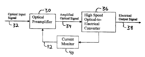
t:apless output power monitoring is generally shown in FIG. 2. An optical
preamplifier 30
amplifies an optical input signal 32 to produce an amplified optical signal
34. The optical
input signal 32 and amplified optical signal 34 are intensity-modulated to
carry data. A
high speed optical-to-electrical (O-E) converter 3ti demodulates the amplified
intensity-
rnodulated optical signal 34 and converts the ampli feed optical signal 34
into an electrical
output signal 38. The O-E convener 36 is generally known in the art and is
preferably a
nigh speed photodetector or a photodetector followed by electrical
amplification.
CA 02408674 2002-10-16
A current monitor 40 monitors a DC bias current of the O-E converter 36, which
is
directly related to the average optical power incident on the O-E converter
36. The current
monitor 40 produces an output power feedback signal 42 proportional to the DC
bias
current. The optical preamplifier 30 adjusts its gain based on the feedback
signal 42 such
that a substantially constant output power is supplied by the optical
preamplifier 30 to the
O-E converter 36. In one embodiment, the optical preamplifier 30, the O-E
converter 36,
and the monitor 40 are implemented in a communications receiver of an optical
transmission system. Other implementations are within the scope of the present
invention.
Because the DC bias current of the O-E converter 36 is monitored to produce
the
output power feedback signal 42, the amplified intensity-modulated optical
signal 34 does
not need to be tapped and monitored. 'Che present invention takes advantage of
the O-E
converter 36 that is already being used to demodulate and convert the
intensity-modulated
optical signal 34. Thus, the system and method of the present invention can
provide
Automatic Power Control (APC) without requiring an output optical tap and a
monitor
1 S photodiode, thereby reducing cost, size, and ma~~ufacturing steps compared
to previous
APC loops. The losses caused by the output optical tap 26 and monitor
photodiode 28 (see
FIG. 1) are also eliminated. Although the present invention employs tapless
output power
monitoring, however, taps may still be used elsewhere in the optical
preamplifier 30.
The optical power is stabilized at the input of the O-E converter 36 (e.g., at
the
active surface of the photodiode), instead of stabilizing optical power at the
output of the
output optical tap 26 (see FIG. 1). As a result, any additional losses (e.g.,
interface losses
and coupling losses) between the output of the optical preamplifier 30 and the
O-E
converter 36 are compensated. Stabilizing the power at the O-E converter 36 is
also
advantageous because this is the data path responsible for the transmission
performance of
the receiver.
Additional embodiments of the present invention are described below with like
or
similar parts identified in the drawings by the same reference characters.
CA 02408674 2002-10-16
Referring to FIG. 3, the O-E converter 36 and the current monitor 40 are
integrated
into an optical preamplifier 50 in cme preferred embodiment. This embodiment
of the
optical preamplifier 50 shows a photodiode bias voltage 44 applied to the O-E
converter
36 for proper operation, as is generally known in the prior art. The current
monitor 40
monitors the photodiode bias current in the O-E converter 36 to produce the
feedback
signal 42. In this embodiment, the optical preamplifier 50 includes an optical
gain
medium 52 for receiving the optical input signal and providing optical gain to
the
amplified optical signal. One type of optical gain medium 52 includes a rare
earth doped
fiber, such as erbium doped fiber used in an erbium doped fiber amplifier
(EDFA). The
optical gain medium 52 is pumped using a pump laser 54, which is controlled by
pump
bias control circuitry 56. Other types of optical gain media and optical
amplification
techniques known in the art are also contemplated.
Referring to FIG. 4, one embodiment of the optical preamplifier 50 is shown in
greater detail. According to this embodiment, the photodiode bias current of
the O-E
converter 36 is monitored by a current sensing resistor 60 and a differential
amplifier 62.
The voltage from the output of the differential amplifier 62 is proportional
to the incident
optical power of the O-E converter 36 and provides the feedback signal 42. In
this
embodiment, the pump bias control circuitry 56 includes an integrator 66 and a
laser diode
pump driver circuit 6~. The voltage from the output of the differential
amplifier 62 is
compared with a reference voltage V~EF at the input of the integrator 66. The
output
voltage of the integrator 66 is fed back to the pump driver circuit 6$,
correspondingly
adjusting the gain of the optical preamplifier 50.
This exemplary embodiment of the optical preamplifier SO shown in FIG. 4 and
described above is one possible circuit implementation. Other circuit
implementations of
the optical preamplifier are also within the scope of the present invention.
Another embodiment of the current monitor 40 is shown in FIG. 5. This circuit
implementation allows the photodiode bias voltage of the O-E converter 36 to
be kept
relatively constant over a larger possible operating range of optical power
for proper
photodetector operation. The voltage at VRer in the circuit is set using the
appropriate
CA 02408674 2002-10-16
resistor values to the optimum bias voltage VB;as for the particular
photodetector. Thus, the
reference voltage VR~f~ at the positive input of the operational amplifier 70
sets the bias
voltage VB;as of the photodetector of the O-E converter 36.
The bias current (1b) of the photodetector runs through the resistor (R) ?2
and is
mirrored proportionally through the resistor (kR) 74 by an operational
amplifier 76. The
values of the resistors 72, 74 are proportional with the proportion depending
on the
constant (k) chosen. Both of these resistors 72, 74 are preferably chosen
appropriately to
minimize power consumption, ensure sufficient voltage headroom for proper
operation of
the circuit, and ensure that a voltage drop at the minimum optical input power
is
significantly greater than any offsets of the optical amplifiers in the
circuit. The collector
current of the transistor 78 reproduces this mirrored current, which flows
through the
resistor (R4) 80, producing a voltage proportional to the photodetector bias
current (Ib)
and to the optical input power (i.e., V~,~,,---kP;~). An operational amplifier
82 at the output of
the circuit buffers this voltage, wluich is sent as the feedback signal to the
pump bias
control circuitry as described above.
This exemplary circuit shown in FIG. 5 and described above is one possible
implementation of the topless output power monitoring in an optical
preamplifier. Other
circuit implementations for the current monitor are also within the scope of
the present
invention. This reduces cost, complexity and losses and also allows additional
losses to be
compensated.
According to the various embodiments of the present invention, therefore,
output
power monitoring can be implemented in an optical preamplifier without the use
of an
output optical tap and monitoring photodiode.
Modifications and substitutions by one of ordinary skill in the art are
considered to be
within the scope of the present invention, which is not to be limited except
by the following
claims.