Note: Descriptions are shown in the official language in which they were submitted.
CA 02408896 2002-10-18
1
SUPERCONDUCTING POWER CABLE WITH ENHANCED SUPERCONDUCTING
CORE
BACKGROUND OF THE INVENTION
Field of the Invention
The instant invention relates to the conduction of electric
power and particularly to the manufacturing of a
superconducting power cable of at least one phase,
characterized by a central core based on a superconducting
tape material BSCCO of 22233 (Bi2 Sr2 Cat Cu3 O,) commercial
composition giving a minimum current density of 7 KA/cm2
under the criteria of I pV/cm. It also includes an annular
space of thermal insulation system wherein the corrugated
casing of the system presents a vacuum pressure below 10 mPa
(milliPascals) permitting the thermal insulation to maintain
operating temperatures of 77 K (temperature of liquid
nitrogen under atmospheric pressure) throughout the cross
section of the cable in its superconducting part.
Previous Art
The invention relates to the transportation of electric
power in superconducting conditions, zero resistance in
direct current. This invention replaces the use of power
cables for distribution and transmission in voltages from 15
kV upwards because it presents lower conduction losses.
High temperature superconductors can be important aspects o
technological advances, because equipment and devices coula
CA 02408896 2002-10-18
have superconducting parts in their components. An obvious
application in superconducting state is the use of zero
resistance properties to the passage of direct current and
low power losses in the electricity transmission. In the
present transmission lines, electric power is lost through
heat when the current passes through normal conductors. If
electricity is transmitted through superconducting cables,
said losses can be reduced or eliminated with the subsequent
savings in the energy costs. This can be applied to any
electric component having cooper leads, for examples,
motors, transformers, generators and any equipment involved
with electric power.
Some US and Japanese companies have manufactured and
evaluated superconducting cable models of up to 5000 cm
obtaining current values not exceeding 1700 A to 2000 A.
Tests conducted in 5000 cm long segments have shown problems
related to current distribution among layers. Said
distribution tends to be irregular because of
electromagnetic problems related to the lead itself.
Patent WO 00/39813 describes a superconducting cable using
high temperature superconducting materials HTS with flexible
core. However it applies to a traditional coaxial design
with insulated HTS tape layers and cold design.
Japanese Patent 06239937 A2 describes a superconducting
cable with HTS materials and flexible core but involving a
CA 02408896 2011-03-07
54006-10
3
traditional DC (direct current) design and insulation between each HTS tape
layer.
Patent US 5,929,385 describes a superconducting cable similar to the object of
the
instant invention but only as far as the type of materials used is concerned.
US
Patent 5,952,614 also describes a superconducting cable similar as far as the
use of
HTS materials and flexible core are concerned but with a coaxial design, in
cold
conditions and with HTS tape traditional design. For these reasons, said
inventions
are different from the characteristics of the instant invention.
DESCRIPTION OF THE INVENTION
According to one aspect of the present invention, there is provided a
superconducting
power cable comprising: a central superconductivity core comprising a first
flexible
corrugated pipe; a plurality of stainless steel tape layer around the core; a
plurality of
copper tape layer surrounding the stainless steel tape layer; a plurality of
superconducting material on the copper tape layer; a wrapping tape comprising
an
insulating material on the superconducting material; a vacuum thermal
insulation
system comprising a flexible corrugated pipe on the insulating material; a
plurality of
thermal insulation layer applied on the periphery of the flexible corrugated
pipe; a
second flexible corrugated pipe on the thermal insulation layer, which forms a
vacuum space; a braided stainless steel mesh on the external wall of the
second
flexible corrugated pipe; a first semiconducting shield around the stainless
steel mesh
surface; an electric insulation on the first semiconducting shield; a second
semiconducting shield on the electric insulation; a metal shield on the second
semiconducting shield; and a protective casing on the metal shield.
According to another aspect of the present invention, there is provided a
method of
providing zero resistance property to the passage of direct current and low
power
losses in electric transmission comprising the use of a superconducting cable
as
described above.
CA 02408896 2011-03-07
54006-10
3a
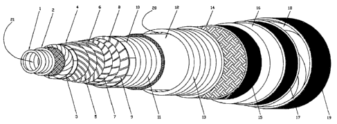
Hereinafter the invention will be described in connection with the drawings of
figures 12 to 6, wherein:
Figure 1 is a perspective view with cross section showing the different
layers of the super conducting power cable.
Figure 2 is a cross section view of Figure 1.
Figure 3 is a perspective view with cross section of the vacuum section
of the central core thermal protection.
Figure 4 is a perspective view with cross section of Figure 3 showing
the opposite wall of the thermal insulation.
Figure 5 is a perspective view with cross section of the superconducting
power cable core.
CA 02408896 2002-10-18
4
Figure 6 is a perspective view with longitudinal cross
section of Figure 1, showing the annular space of
thermal insulation.
The invention is related to the transportation of
electricity in superconducting conditions, (zero resistance
in direct current). This invention replaces the use of power
cables for distribution and transmission in voltages of 15
kV or more because it presents lower conduction power
losses, considering that for a Cu lead with a current
density of 1 - 4 A/mm2 and a resistivity of 2 x 10⁻⁸ S2m, the
transmission losses are on the order of 20 - 80 mW/Am. To
better compare with superconducting cables, losses caused by
the heating of superconducting materials have to be taken
into account. At cryogenic temperatures, said losses are
defined by a Carnot factor divided between the efficiency of
the cooling system. In the case of liquid nitrogen, this
factor is between 10 and 20. Thus, in a superconductor
losses will be lower than 5 mW/Am. The flow of liquid
nitrogen fills the longitudinal cavity 21, Fig. 5, of the
flexible corrugated pipe 1 of 304 or 316 stainless steel.
Said pipe can have an external diameter between 2 cm and 6
cm and an internal diameter between 1 cm and 4 cm wherein
the depth of the corrugation can vary between 0.5 cm and
cm. The corrugation pitch can be between 0.8 and 1.5 cm for
a corrugation depth between 0.4 and 0.5 cm. As another
CA 02408896 2003-09-11
alternative for a depth between 0.4 and 0.6 cm, the
corrugation pitch can be between 1.6 and 3 cm. On this pipe,
a 304 or 316 stainless steel mesh is placed in order to
5 obtain a relatively flat surface. On this mesh a stainless
steel tape layer 2 is placed, between 4 and 5 cm wide and
between 0.0005 and 0.006 thick. They are placed on the
corrugated pipe with spacing between 0.15 and 0.2 cm. Then
one or two additional stainless steel tapes, 2.5 to 4 cm
wide and 0.001 to 0.002 cm thick, are placed with spacing
between the tapes of 0.1 to 0.15 cm. After, a first layer of
Cu tapes 3 is placed, from 0.25 to 0.40 cm wide and from
0.025 to 0.030 cm thick, with a cabling length between 2 cm
and 100 cm depending on the design of the first layer of
superconducting tapes to be applied. Said layer of Cu tapes
can be laid at an angle ranging from 00 to 45 depending on
the cable design. The superconducting material to be used is
made of tapes of a 22233 (Biz SR2 Ca2 Cu3 OX) composition
commercial product BSCCO. Said tapes range in width between
0.38 and 0.42 cm and in thickness between 0.018 and 0.22
cm, which gives a minimum current density of 7 kAcm2 under
the criteria of 1 V/cm, (microvolt/centimeter). With this
superconducting material, two or more layers of tapes are laid
with a cabling lay length between 20 cm and 300 cm, at
an angle ranging from 0 to 45 depending on the design of
each layer with a direction that can be right or left 4, 5,
CA 02408896 2002-10-18
6
6. And two or more layers of superconducting material tape
with a lay length between 20 cm and 300 cm with an angle
ranging from 0 to 45 depending on the design of each layer
with a direction that can be right or left with regard to
the cabling, in the opposite direction of the previously
placed layers 7, 8, 9. Finally, a wrapping tape made of
insulating material 10, with a thickness ranging between
0.005 and 0.01 cm and a width ranging between 2 and 4 cm is
laid.
In order to protect the central core, the superconducting
power cable object of the instant invention is also
characterized because it includes a vacuum thermal
insulation system consisting of a flexible corrugated pipe
11 made of 304 or 316 stainless steel, to hold the
superconducting cable and liquid nitrogen. Said pipe can
have an external diameter ranging between 4 cm and 8 cm and
an internal diameter ranging between 3 cm and 7 cm, the
corrugation depth varying between 0.5 cm and 1 cm. The
corrugation pitch can vary between 1 cm and 2 cm for a
corrugation depth between 0.5 and 0.8 cm. Then, on the
periphery of this pipe, a multi layer thermal insulation (Pa)
12 is applied, which can have a thickness ranging between
0.0005 cm and 0.005 cm which is calculated according to the
following formula:
CA 02408896 2002-10-18
1
Pa = (Ss + Prtr) (N/Ax)
wherein:
Pa Thickness of the insulating layer
S, Mass of the material per area unit
pr Insulating material density
tr Thickness of the anti-radiation casing
N/Ax Layer density
Concentrically around the flexible corrugated pipe 11,
covered with the insulating material 12, a second corrugated
pipe 13 is placed, creating the vacuum thermal insulation
space 20, Figure 6.
To ensure the adequate functioning of the thermal insulation
system at a temperature of 77 K, a vacuum pressure below 10
mPa (milliPascals) is required.
Said second corrugated pipe 13, which creates the vacuum
space, is made of 304 or 316 stainless steel which can have
and external diameter ranging between 8 cm and 10 cm and an
internal diameter ranging between 6 and 7 cm, wherein the
depth of the corrugations may vary between 0.5 cm and 1.5
cm. The corrugation pitch can be between 1 and 2 cm for a
corrugation depth between 0.5 and 1 cm.
CA 02408896 2011-03-07
54006-10
8
The thermal insulation system includes also on the external wall of the
corrugated
pipe 13, a braided stainless steel mesh 14, Fig. 1 and 3, offering a uniform
surface to
the external wall structure of the helical or spiral shaped corrugated pipe.
Around the uniform mesh surface 14, an internal semiconducting shield 15 is
applied,
which is made of low density thermoplastic polyethylene or any other
thermoplastic or
thermosetting semiconducting material. The conductivity of said shield should
not
exceed 1000 S2m when it is measured at room temperature, said shield having a
thickness of at least 0.006 cm. On this semiconducting shield the electric
insulation
of the cable 16 is placed. Said electric insulation is based on low, medium or
high
density, thermoplastic or thermosetting or crossed chain polyethylene and/or
Ethylene Propylene (EP), the thickness of the insulation being between 0.229
cm and
0.976 cm depending on the operation voltage level of the cable. On this
electric
insulation, a second semiconducting shield 17 made of the same materials as
the
internal semiconducting shield 15 is placed, Figure 4. However, in this case,
the
thickness of the shield must be at least 0.0129 cm and has to fulfill a
maximum
volume resistivity of 500 Qm when measured at room temperature. On this layer,
a
metal shield made of Cu
CA 02408896 2002-10-18
9
tape 18 is placed, which must be at least 0.0635 cm thick,
having a cross section area of at least 0.1 mm2/mm. On this
metal shield 18, a protective casing 19 is placed, possibly
made of polyethylene or polyvinyl chloride (PVC) depending
on the application of cable, said casing having a thickness
ranging between 0.203 and 0.279 cm.
According to the technical requirements, the basic
superconductor design parameters used were as follows:
* Tape Width (cm): 0.4 t 0.02
* Tape Thickness (cm): 0.02 t 0.002
* Critical current Density (kA/cm2)>7 (criterion of
1 V/cm)
* Filamentary section thickness inside the tape
2bec (cm) : 0.018
* Critical current in the bending deformation voltage
value: 0.1% - not below 95% or 0.2% - not below 90%.
* About 20% reduction in the critical current when the
field is between OT and 0.1T.
The basic equations to compute the number of
superconducting tapes and the design parameters are as
follows:
CA 02408896 2003-09-11
Number of tapes per layer (Ni)
Ni = TrxDioxCOS)%
2ai(1 +Si)
5 wherein:
Dio = average diameter of the i layer
2ai = Tape Width of the i layer
Si = Relative space between the tapes of the i layer
Ri = Laying angle of the superconducting tapes
10 Lay of the tapes in a layer (Pi)
PI= nxDio
tan/ii
Relative spacing between the tapes of a layer: (Si)
Sf = nxDioxCos ii
2aixNi
Relative deformation voltage Ei regarding the superconductor
in bending conditions of the tapes is:
St = 2bscx sen Q / Dio
the model base of the superconducting high temperature cable
has been developed, which consists of the design of the
superconducting core itself, as well as the development of
CA 02408896 2002-10-18
11
insulation based on known and previously developed materials
for use in medium and high voltage power cables.
Example 1
Under the design conditions, the superconducting tape VAC
(Germany) was chosen. Said tape presents a critical current
of 59.8 A to 64.7 A depending on the combination of
thickness and width of the superconducting tape. Based on
these variations, the criteria of linearity of the critical
current density used for the cable optimization and
calculation is not very congruent, and thus a value of the
critical current density in the external magnetic field
equals to cero is accepted as 113 A/cm for cable
calculations. Taking into account said variations, the
followings values were taken as parameters for the
calculation.
* External Diameter of the core Dfe = 5.5 cm;
* Tape thickness 2bt = 0.002 cm;
* Filament section thickness inside the tape 2b3 =
0.018 cm;
* Relative space. between each tape in each. layer S =
0.05.
CA 02408896 2002-10-18
12
The minimum lay of the tapes (maximum angle of tape
laying) is selected based on the limitations imposed by the
deformation voltage threshold with regard to bending, for a
superconductor when the tapes in one layer are bent on a
diameter Di and the tape laying angle (3i is at a maximum
permissible value (E <0.2 %, wherein F. = 2b,,cos(3i/Di) . The
critical current of the cable is expected to be between 6 kA
and 10 kA, under the criteria of 1 gV/cm and the approximate
values of the magnetic field induction on the surface of the
sixth layer being between 0.04 T and 0.07 T. For this reason
for every 0.001 T increase, the critical current reduction
of the tape is expected to be 2% its initial value.
The influence of the deformation voltage on the
superconductor with regard to the value of the tape critical
current during the manufacturing of cable is described in
the comments on Table No. 1.
Table No. 1
Expected manufacturing results
(2a = 0.38 cm, 2b,c = 0.018 cm)
Layer D, a N, I. S,
Number Bending % Tape A REAL Real
Mm A A
CA 02408896 2002-10-18
13
1 1332 0.135 40 42.22 1688.8 0.1667 16723 0.0377
2 17.52 0.103 42 41.54 1744.7 0.1722 1727.6 0.0399
3 42.03 0.043 44 40.85 1797.4 0.1771 1779.8 0.0446
4 51.72 0.035 45 40.17 1807.7 0.1784 1790.0 0.0325
15.82 0.114 42 39.49 1658.6 0.1637 16423 0.0457
6 9.97 0.181 37 38.80 1435.6 0.1417 1435.6 0.0484
I E _ 10132.8 1 10047.6
According to the above table, it can be seen that the
current value depends on the maximum deformation voltage if
and only if it does not exceed the deformation value of 0.2%
which is the critical value of the current. From the results
5 obtained in the above table, we observe that there is
uniform current distribution in every layer, which gives a
current distribution factor Ici/I,, = 1 and a real maximum
critical current value of I,Qõs REAL = 10047 A.
Example 2
However, in Table No. 2, the optimization results of the
cable are presented as the criteria to reach the peak
critical current value and the minimization of the energy
losses under the influence of the flow and axial magnetic
field.
Table No. 2
CA 02408896 2002-10-18
14
Optimization Results
Layer D, Tape laying J, I3 Pr Iere J,
direction
Number Exterior A/cm degrees cm I
Cm
1 5.554 I/1 111.11 24.6 37.89 0.1671 1.0000
2 5.588 I11 109.31 18.6 51.96 0.1716 0.9938
3 5.632 1/1 107.51 7.70 13035 0.1765 0.9859
4 5.676 R/-I 105.71 6.30 160.89 0.1769 0.9941
5.720 R/-1 103.91 21.2 46.15 0.1648 0.9967
6 5.764 R/-I 102.11 35.3 25.48 0.1431 0.9985
E = 5.764 1.0000 0.9948
Maximum current reached Imkx = 10028.5
Total sum of the utilization coefficient in the six layers
Kmx = Gji = 5.96689
5 And according to the above mentioned criteria, current
distribution is uniform in all the cable layers, and the
losses caused by the axial magnetic field are minimized.
Wherein:
Di exterior = external diameter of the i layer
CA 02408896 2002-10-18
Jci = Density of the lineal critical current for the
tapes of the i layer
Pi = Tape laying angle for the tapes of the i layer
Pi = Tape lay for the tapes of the i layer
5 Ni = Number of tapes in the .i layer
Ici = Total critical current of all the tapes in the
i layer (current i layer) versus the total number of tapes
(sum of the critical currents of all the tapes) in the
model.
10 Icalc = Ii/Io Current distribution in the i layer of
the total current.
Ni/No = Ici/Ico = Number of tapes in the i layer (critical
current in the i layer) versus the total number of tapes
(sum of the critical currents of all the tapes) in the
15 model.
I,a,, REAL = Real value of the current peak in the i
layer when the current reaches its critical value in at
least one of the layers.
Ji = Superconductor utilization coefficient in
the i layer.