Note: Descriptions are shown in the official language in which they were submitted.
CA 02409411 2002-11-18
WO 01/98788 PCT/USO1/19943
1
RELIABILITY OF YIAS AND DIAGNOSIS BY E-BEAM PROBING
BACKGROUND OF THE INVENTION
[1001] Field of the Invention
[1002] The invention relates to testing of electronic devices. In particular,
the
invention relates to monitoring a net in a device to determine if the net is
the source of
a failure.
(1003] Description of the Related Art
[1004] Chip complexity and increased packaging used in electronic devices are
decreasing device geometries at a rapid pace. Currently, geometries in
electronic
devices have migrated from 0.18 ~m down to 0.13 ~,m. The trend to smaller
device
geometries is expected to continue in the future. As device geometries
decrease,
problems associated with testing and debugging devices continue to become more
difficult.
[1005] To help obviate some of the difficulties of testing these small
geometries, designers are making extensive use of simulation and design
verification
software to eliminate design problems before a device is fabricated. While
simulation
and verification software do identify some design problems before fabrication,
many
designs do not yield fully operational, full specification, parts without
first undergoing
lengthy, and expensive, debug phases. In addition, even if all the design
problems are
identified and corrected prior to fabrication, defects may be introduced into
the device
during the manufacturing process.
CA 02409411 2002-11-18
WO 01/98788 PCT/USO1/19943
2
[1006] During the test and debug process, probing of internal nets of a device
is becoming an increasingly valuable tool. Probing internal nets of a device
assists in
identifying and isolating portions internal to a device that are not
performing properly.
One technique used to provide access to internal nets is to include pads on
some
"critical" internal nets during the design of a device, and thereby allow
access to these
nets during test and debug. However, the vast majority of internal nets will
not have
pads, and therefore no direct access to these nets is possible.
[1007] Packaging density and chip complexity restrict a device designer in
placement of pads on internal nets due to space limitations within the device.
This is
particularly true in very large scale integrated circuits (VLSI) such as gate
arrays, field
programmable gate arrays (FPGA), and application specific integrated circuits
(ASIC)
such as mixed signal integrated circuits. The lack of direct access to all of
the internal
nets of a device complicates the test and debug process.
[1008] Certain aspects of device layout further increases the complexity of
testing and debugging. For example, it is very difficult to detect a defect,
such as a
manufacturing defect, at the bottom of a trench or a via. Typically, detection
of a
defect at the bottom of a trench or via requires a failure analysis of the
device using
instrumentation such as electron microscopes. In addition, intermittent
failures, such
as stress related intermittent failures, are especially difficult to locate
due to their
nonrepetitive nature.
CA 02409411 2002-11-18
WO 01/98788 PCT/USO1/19943
3
[1009] Several techniques have evolved in testing and debugging electronic
devices. Some of these techniques include functional testing, burn-in testing,
and
defect detection.
[1010] Functional testing is typically used to verify proper operation of an
electronic device. For example, an IC may undergo functional testing following
the
completion of the IC fabrication process. Test leads, or probes, are connected
to the
Input and Output (I/O) pins of the IC. Test stimuli are applied to input pins
of the
IC and the output pins of the IC are monitored to determine if expected
signals are
produced. Functional testing is typically performed under normal ambient
conditions,
so that the device under test is not being exposed to any type of external
stress, for
example, environmental stress such as elevated temperature.
[1011] Another technique used in testing and debugging electronic devices is
burn-in testing. Typically, a burn-in test of a device involves elevating the
ambient
temperature of a device that has power applied. A burn-in test will stress the
entire
device, including all nets within the device. Due to the environment that the
device is
being tested in, it may not be practical to decapsulate a device to expose the
internal
nets of the device due to environmental concerns, such as, condensation in the
device.
Furthermore, even if the device could be decapsulated, making the internal
nets of the
device accessible, failure of an individual net may be difficult to identify
through burn-
in testing because the entire device and all nets are stressed equally.
[1012] A third technique, defect detection, monitors the device I/O pins as
well as probes internal nets of the device. Typically, probing internal nets
of a device
CA 02409411 2002-11-18
WO 01/98788 PCT/USO1/19943
4
requires that the device be decapsulated, thereby providing access to the
internal nets.
Because the device is decapsulated, environmental stressing of the
decapsulated device
may be impractical.
[1013] One technique used to probe internal nets uses mechanical probes.
Mechanical probes may be aligned, and physically contact an internal net of
the
device. One drawback to using mechanical probes is that they may load the
electrical
circuit of a net being tested. For example, the mechanical probes may increase
circuit
capacitance and therefore distort the measured performance of the circuit from
how
the circuit would perform without the added loading of the mechanical probes.
[1014] A technique that has been developed to eliminate loading of a circuit
of
a device under test is an electronic-beam (e-beam) probe. Recent development
of e-
beam probe tools and techniques have greatly assisted in overcoming some of
the
problems involved in probing internal nodes of electronic devices for debug
and other
purposes.
[1015] E-beam probing uses the principle of voltage contrast in a scanning
electron microscope (SEM). A conventional SEM image is produced by raster-
scanning a finely-focused beam of primary electrons over a device under test
as signals
are applied to the device. Secondary electrons are produced as the primary
beam is
reflected from the device under test. The secondary electrons reflected from
the
device are measured and, using a scintillator, photo-multiplier tube (PMT) and
associated electronics, an image of the nets of the device under test is
produced. The
energy of the secondary electrons produced by the device under test results
from
CA 02409411 2002-11-18
WO 01/98788 PCT/USO1/19943
variations in the electrical potential on the surface of conductors, or nets,
within the
device. Secondary electrons that strike the face of the scintillator produce a
number of
photons proportional to the energy of the secondary electrons, which are
emitted
from the scintillator and strike the face of the PMT. The PMT outputs a
voltage
proportional to the number of photons that strike its face. The voltage out of
the
PMT is amplified by associated electronics and used to produce an image that
corresponds to the electrical potential on the surface of the conductors and
nets within
the device. In this way, the e-beam technique provides an indication of node
voltages.
[1016] For example, positive voltages may appear as dark areas in the image,
corresponding to a low secondary electron count. Zero, or negative, voltages
may
appear as light areas in the image, corresponding to a higher secondary
electron count.
[1017] E-beam probing offers several advantages over other probing
techniques, such as mechanical probing. An e-beam probe is typically passive,
meaning that it does not interact or load the electrical circuit that is being
monitored.
In contrast, as mentioned above, mechanical probes may load the circuit being
tested,
making measurements inaccurate.
[1018] Therefore, there is a need for an effective way to monitor the
operation
of internal nets of an electronic device, without affecting the operation of
the device,
identifying particular nets that may be the source of failure.
CA 02409411 2002-11-18
WO 01/98788 PCT/USO1/19943
6
SUMMARY OF THE INVENTION
[1019] Identifying a failure net in an integrated circuit (IC) whose output
indicates an IC failure includes determining a potential failure net by
observing a signal
produced by the net that indicates failure, stressing the potential failure
net while
leaving other IC nets unaffected, and observing a change in the signal
produced by the
potential failure net in response to the stress, thereby identifying the
potential failure
net as a failure net of the IC.
[1020] Stressing a net in a device, or IC, may include aligning an external
source of stress to the net, applying stress to the net while leaving other
device nets
unaffected, and monitoring the net, while the stress is being applied, to
determine if
the net fails while it is being stressed.
[1021] Locally stressing a net in a device, or IC, may include aligning an e-
beam probe onto a suspect net within the device. Once the e-beam probe is
aligned
with the suspect net, the current in the e-beam is increased, thereby locally
applying
stress the device near the suspect net.
[1022] Other features and advantages of the present invention should be
apparent from the following description of the preferred embodiment, which
illustrates, by way of example, principles of the invention.
CA 02409411 2002-11-18
WO 01/98788 PCT/USO1/19943
7
BRIEF DESCRIPTION OF THE DRAWINGS
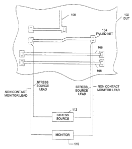
[1023] Figure 1 is a diagram of a portion of a device under test, and test
equipment, illustrating aspects of a system constructed in accordance with the
invention.
[1024] Figure 2 is a schematic of an exemplar circuit illustrating trace-back.
[1025] Figure 3 is a block diagram of a test station used in accordance with
the
invention.
[1026] Figure 4 is a block diagram showing additional detail of the e-beam
column.
[1027] Figure 5 is a graph illustrating the output waveforms of a typical two
phase clock generator and the clock generator under test.
[1028] Figure 6 is the artwork of a portion of the device around the failing
net.
[1029] Figure 7 is an scanning electron microscope (SEM) picture of the
suspected failing via.
[1030] Figure 8 is a tunneling electron microscope (TEM) picture of the
suspect via near the tungsten-metal interface.
DETAILED DESCRIPTION
[1031] In a typical integrated circuit (IC) electronic device, such as a very
large
scale integration (VLSI) chip, there are many interconnections and vies
internal to the
device. Most of the internal connections and vies of the IC are not directly
accessible
by a mechanical probe. It may not be practical to identify a particular net
for failure
CA 02409411 2002-11-18
WO 01/98788 PCT/USO1/19943
without monitoring the nets of an IC while the device is being exercised by a
test
signal. An initial step in a failure analysis of a device is to determine the
location of
the failure. As discussed above, probing internal nets is challenging.
Mechanical
probes tend to load the electrical circuit being monitored, and thus may
provide
inaccurate, and nonrepeatable, measurements. Therefore, a non-contact,
repeatable
measurement technique for monitoring internal nets of a device is desirable.
[1032] One type of non-contact, repeatable, measurement unit for monitoring
internal nets of a device is an electronic-beam (e-beam) probe. Typically, an
e-beam
probe will be mounted on a positioning device to provide coarse alignment of
the e-
beam with a desired net within the device. If the positioning device
controller has
access to the device layout database the positioning device will be able to
automatically locate pre-identified nets within the device. Fine alignment of
the e-
beam is typically accomplished with focusing coils, or an objective lens, as
discussed
below.
[1033] In addition to monitoring an internal net, it may also be desirable to
apply stress locally to the device, for example to stress only one net of the
device
under test. By stressing only a desired net, and not affecting other nets, a
failure mode
of a device may be isolated and identified. For example, if an individual net
has a
failure that is temperature dependent, then by being able to stress the
individual net it
may be possible to reliably determine if the stressed net is the source of the
failure.
[1034] Figure 1 is a diagram of a portion of a device under test 102, and test
equipment, illustrating aspects in accordance with the invention. A portion of
the
CA 02409411 2002-11-18
WO 01/98788 PCT/USO1/19943
9
device under test 102 is illustrated showing a plurality of internal nets and
vias. As
described below, one of the nets has been identified as a potential failure
net 104, and
the other, remaining, nets 106 are believed to be operating satisfactorily.
Test stimuli
are applied to the I/O pins of the device under test 102 and signals on the
nets 104 and
106 vary accordingly.
[1035] In one embodiment, the signals on the potential failure net 104 are
monitored using a non-contact measurement device 110, for example, an e-beam
probe.
In addition, a stress source 112 is aligned with the failure net 104. The
stress source is
configured to apply a source of stress, for example, temperature, current, or
voltage.
[1036] In another embodiment, the stress source uses mechanical probes,
configured to minimize any loading of the electrical circuit, to apply the
stress. In
another embodiment, the stress source uses non-contact probes, such as e-beam
or
laser light, to apply the stress.
[1037] In yet another embodiment, the stress source 112 and the non-contact
measurement device 110 are the same unit, for example, a single e-beam probe
configured to monitor potential failure nets as well as to apply stress. For
example,
the current density of the primary beam from the e-beam probe may be increased
from
a nominal value of about 1 nAmp used to monitor the net to a value of about 50
nAmps used to apply stress. In contrast with conventional use of an e-beam
probe,
by increasing the current density in the e-beam probe, the probe is no longer
just a
passive monitoring device. Instead, the e-beam probe is actively interacting
with the
net by applying a localized stress to the net, while at the same time
monitoring the
CA 02409411 2002-11-18
WO 01/98788 PCT/USO1/19943
reflected secondary signal from the net. In all these embodiments, the stress
is applied
to a single potential failure net while the net is being exercised by a test
input and
monitored.
[1038] In accordance with the invention, a variety of trace-back techniques
5 may be used to identify a potential failure net. Trace-back is a systematic
testing of
nets beginning at a location in the device that has an identified failure, for
example a
failure at an output of a device found during functional testing. For example,
if a
failure is detected at an output node of a portion of an electrical circuit,
then the input
nets to that portion of the electrical circuit are tested. If all the input
nets to the
10 portion of the electrical circuit test "good" then the failure is isolated
to that portion
of the electrical circuit identified. If one, or more, of the input nets to
the portion of
the electrical circuit are identified as failing, then testing proceeds back
to the electrical
circuitry that is the source of the failing input net. Testing continues until
the failing
portion of the electrical circuitry is isolated.
[1039] Figure 2 is a schematic diagram of an exemplary circuit, of an IC
device
200, illustrating a trace-back technique that was applied to identify a net.
For this
illustration an unstable digital circuit in an IC, for example a mixed signal
VLSI device,
is described. In Figure 2 the digital value output by a register 202, _ as
measured on the
net 204, is indicating a circuit failure. To determine if the failure is in
the register 202
or the net 204, the input signals to the register 202, and the nets 206, 208,
210, 212
and 214, are monitored. In this example, nets 206, 208, 210 and 212 tested
satisfactorily, while net 214 had a failure. Because the net 206 tested
satisfactorily,
CA 02409411 2002-11-18
WO 01/98788 PCT/USO1/19943
11
the circuit device 220 feeding the net 206, and the nets feeding the circuit
device 220,
are not tested further. The nets feeding the circuit device 222 are tested to
determine
if there is a failure on a net feeding the circuit device 222 or if the
circuit device 222 is
causing the failure.
[1040] The inputs to the circuit device 222 are nets 230, 232, 234 and 236. In
this example nets 230, 232 and 234 tested successfully and net 236 failed.
Because
nets 230, 232 and 234 tested successfully, additional testing of the circuitry
feeding
these nets is not performed. Because net 236 failed, the nets feeding the
circuit device
240 are tested to determine if there is a failure on the nets feeding the
circuit device
240 or if the circuit device 240 is causing the failure.
[1041] The inputs to the circuit device 240 include nets 250, 252, and 254. In
this example nets 250, 252, and 254 tested successfully. Thus, the trace-back
testing
has isolated the failure to either the circuit device 240 or net 236. To
determine if the
circuit device 240 is failing or if net 236 is failing additional testing is
performed where
net 236 is locally stressed, without stressing the circuit device 240 or any
other circuit
devices, or nets, in the IC device 200. By stressing the net 236 it may be
possible to
isolate the failure to the individual net 236.
[1042] As discussed above, reliability of via structures in VLSI devices is a
major concern in the fabrication of semiconductor devices. In particular,
tungsten via
structures in aluminum alloy interconnect systems have been susceptible to a
high
level of failure. As discussed above, failure analysis of via defects is an
ever increasing
challenge. Aspects of the invention are discussed next in relation to a
failure analysis
CA 02409411 2002-11-18
WO 01/98788 PCT/USO1/19943
12
performed on an unstable digital circuit that caused intermittent failures in
a mixed
signal VLSI device. The failure analysis on this device revealed a via
structure
containing voids and an anomalous thin layer under the Ti/TiN adhesion layer
at the
interface of a tungsten plug and the underlying AlCu alloy.
[1043] The unstable digital circuit was part of a mixed signal device that
included both digital and analog circuitry. The device had passed wafer
probing and
final testing, and thereafter was shipped to the field. In the field the
device exhibited
intermittent failures. The device was returned from the field and a
conventional failure
analysis was performed. Multiple manual probing techniques were attempted
without success to analysis the failure mode. A problem with the mechanical
probing,
as discussed above, was that the mechanical probe loaded the electrical in the
device
that was being tested. Loading of the circuit being tested produced
inadequate,
unreliable, test results. To eliminate the loading produced by the mechanical
probes, a
non-contact technique, using an e-beam probe in accordance with the invention,
was
implemented to perform the failure analysis of the device.
[1044] Figure 3 is a block diagram of a test station 300 used in accordance
with
the invention. The test station includes an e-beam probe unit 302, such as the
Schlumberger IDS10000p1us. The test station includes a workstation 303 used by
the
test operator to control the test equipment, as well as to provide a visual
display of
the test results to the operator.
[1045] The e-beam probe unit 302 includes a load module 304 that holds the
device under test and provides electrical connection to the I/O pins on the
device. The
CA 02409411 2002-11-18
WO 01/98788 PCT/USO1/19943
13
load module 304, after the device under test has been mounted to it, is
secured to the
specimen chamber lid 306. Prior to mounting the device under test to the load
module
304, the device has the top portion of its encapsulation removed. This exposes
the
internal structure of the device, including the internal nets. When the load
module 304
is secured to the specimen chamber 306, the device under test is positioned
facing
downward, with the exposed internal structure facing into the specimen chamber
308.
[1046] At the bottom of the specimen chamber 308 there are two ion pumps
310 and 312. The ion pumps 310 and 312 are used to produce a vacuum within the
specimen chamber. At the end of the specimen chamber 308 opposite the device
under test is an e-beam column 320. As discussed below, the e-beam column
generates an electron beam that is focused onto the device under test for
monitoring
voltages on internal nets of the device. The e-beam column 320 and ion pumps
310
and 312 are mounted to an XY stage 322. XY stage 322 allows for coarse
alignment of
the electron beam generated by the e-beam column with the internal nets of the
device
under test.
[1047] Figure 4 is a block diagram showing additional detail of the e-beam
column 320. The e-beam column 320 includes a filament 402. The filament 402
generates electrons used to produce the e-beam. The electrons emitted by the
filament
402 are accelerated by an electrostatic lens 404 toward the device under test
102.
After the electrons pass through the electrostatic lens 404, the electrons are
focused
into a beam by a condenser lens 408. The electron beam passing through the
CA 02409411 2002-11-18
WO 01/98788 PCT/USO1/19943
14
condenser lens 408 travels through the vacuum in the specimen chamber towards
the
device under test 102.
[1048] As the electron beam nears the device under test 102 it passes through
an objective lens 410. The objective lens 410 focuses the electron beam into a
primary
electron beam that is directed onto the desired internal net of the device
under test
102. The primary electron beam interacts with the internal net of the device
under
test 102, and secondary electrons are emitted back into the specimen chamber.
[1049] Located between the condenser lens 408 and the objective lens 410 is a
detector 420. The detector 420 includes a scintillator 422. The scintillator
422 emits
photons, in proportion to the energy of the secondary electrons, when the
secondary
electrons strike its face. The photons emitted by the scintillator 422 are
directed to a
photomultiplier tube (PMT) 424. The PMT 424 is configured to generate a
voltage
proportional to the number of photons that strike its face. Thus, the PMT 424
output voltage is proportional to the energy of secondary electrons emitted by
the
internal net in the device under test. The PMT 424 output voltage is sent to
an
amplifier 426 where the signal is amplified and conditioned. The amplifier 426
signal
output is routed to the workstation 300 where it is processed and a display is
generated for the operator.
[1050] As discussed above, the display is an image that represents the
intensity variations of the secondary beam due to the electrical potential on
the
surface of conductors, or nets, within the device. For example, positive
voltages may
appear as dark areas in the image, corresponding to a low secondary electron
count.
CA 02409411 2002-11-18
WO 01/98788 PCT/USO1/19943
1S
Zero, or negative, voltages may appear as light areas in the image,
corresponding to a
higher secondary electron count.
[1051] The test setup described above was used to test the failed mixed signal
device. Using trace-back techniques with an e-beam probe, the device failure
was
S narrowed down to an individual 8-bit right-shift register used for digital
data input.
Additional testing revealed that data signals from the 8-bit register failed
to match pre-
assigned ID codes. The failure of the signals out of the 8-bit register were
believed to
be a cause of the functional failure of the device.
[1052] To assist in identifying the failure mechanism of the device, all the
register related nets were measured using the e-beam probe. The e-beam probe
testing
revealed that a two phase clock generator in the digital circuitry produced
irregular
waveforms. Figure 5 is a graph illustrating the output waveforms of a typical
two
phase clock generator and the clock generator under test. Traces S 10 and S 12
illustrate
satisfactory clock generator output signals from a known good device. Traces
520 and
1 S S22 illustrate the output signals of the clock generator under test. Trace
S22 is
irregular, being nearly triangular rather than the expected squarewave shape.
[1053] Additional e-beam probing of all the internal nets of the clock
generator
localized the failure to an output inverter (buffer) of the failed clock
generator.
[1054] After identifying the failed output inverter as a possible failure, the
nets of the output inverter were locally stressed. The techniques used to
locally stress
the nets used in this example included increasing the current in the e-beam,
and
increasing the electron flux of the e-beam. During the testing of the mixed
signal device,
CA 02409411 2002-11-18
WO 01/98788 PCT/USO1/19943
16
the test station 300 was operated to increase the current in the e-beam from
about 1
nAmp to monitor the net, to about 50 nAmps to stress the net. In addition, a
higher
magnification of the e-beam through the objective lens 410 of the e-beam
column 320
was used to concentrate the e-beam onto a smaller area of the net, thereby
increasing
the electron flux.
[1055] Traces 530 and 532 illustrate the clock generator output signals while
undergoing localized thermal stress. As traces 530 and 532 illustrate, it was
discovered that the clock generator output suffers severe distortion, no
longer
oscillating, when thermally stressed.
[1056] Simulations were performed using high via resistance on the output net
of the failing inverter. The simulation produced a signal similar to the
triangular trace
522 measured with the e-beam probe. Further simulation increased the via
resistance
to a very high value, and the inverter output stopped switching, similar to
traces 530
and 532. Because traces 530 and 532 were made when the net was being subjected
to
thermal stress, it was believed that the thermal stress may have caused the
net
resistance to increase to a very high value.
[1057] Figure 6 is the artwork of a portion of the device around the failing
net.
The net includes two vies 601 and 602. It was believed that the vies may be
the cause
of the high resistance.
[1058] Bonding pads were then placed across the suspect vies 601 and 602
using a focused ion beam (FIB) technique. A very high resistance across the
via was
confirmed. Additional failure analysis was performed using a scanning electron
CA 02409411 2002-11-18
WO 01/98788 PCT/USO1/19943
17
microscope (SEM) and one of the suspect vial 601 and 602 was identified as a
suspected failing via. Figure 7 is an SEM picture of the suspected failing
via. Figure 7
reveals a void 702 of about 0.2 ~,m in the Al-alloy underneath the tungsten
layer.
[1059] Further failure analysis was performed on the suspect via using a
tunneling electron microscope (TEM). Figure 8 is a TEM picture of the suspect
via
near the tungsten-metal interface. Figure 8 reveals a very thin anomalous
layer 802 of
about 150 angstroms below the Ti/TiN adhesion layer underneath the tungsten
plug.
It is believed that the anomalous layer was aluminum oxide from de-ionized
(DI) water
corrosion during a via cleaning process after a via etch, during the
manufacturing
process.
[1060] A poor tungsten-metal interface may cause via delamination and
enhance localized thermal stress. In addition, poor tungsten-metal interface
may
accelerate the formation of voids in the AICu alloy underneath a tungsten plug
during
high temperature processes or localized electrical thermal stress. The
formation of
voids in the Al-alloy underneath the tungsten layer can be explained by the
discontinuity in Al flux at the tungsten-AlCu interface. For example, Al flux
leaving
from the hot area may not be compensated from the tungsten plug during
electromigration.
[1061] Voids and a thin anomalous layer at the tungsten-AICu interface can
cause severe degradation in tungsten-AICu interconnect systems. The
degradation
may lead to either permanent device failures or intermittent functional
failures,
depending on the degree of the degradation and the amount of electrical
thermal stress
CA 02409411 2002-11-18
WO 01/98788 PCT/USO1/19943
1$
in the affected interconnects during certain testing or application
environments. The
tungsten-AICu interconnect system is one of the major reliability problems in
VLSI
devices, especially with current semiconductor process technologies.
(1062] In the device under test described in the above example, new via
cleaning processes were implemented by the manufacturer to reduce the DI water
corrosion and to minimize thermal stress induced voiding in the tungsten-AICu
interconnect systems. The reliability of the via interconnect has been
improved
following the change in process. To date, no similar intermittent device
failure has
been observed. Thus, the technique successfully identified a source of failure
in the
mixed signal device, and appropriate remedial action was able to be
undertaken, as a
result of the isolated circuit stress and net monitoring.
[1063] The foregoing description details certain embodiments of the invention.
It will be appreciated, however, that no matter how detailed the foregoing
appears, the
invention may be embodied in other specific forms without departing from its
spirit or
essential characteristics. The described embodiments are to be considered in
all
respects only as illustrative and not restrictive and the scope of the
invention is,
therefore, indicated by the appended claims rather than by the foregoing
description.
All changes which come with the meaning and range of equivalency of the claims
are to
be embraced within their scope.