Note: Descriptions are shown in the official language in which they were submitted.
CA 02409578 2002-10-22
1
FILM FOR A FILM CAPACITOR AND FILM CAPACITOR
Technical field
The present invention relates to a film for a film
capacitor according to the preamble of claim 1 and to a
film capacitor and a method for producing a film for a
film capacitor.
Prior art
The invention concerns film capacitors. In addition, it
can also be used for other elements of electrical
engineering, for example for bushings of transformers
or switches and insulation systems of cables and cable
end terminations, and also for ceramic and other
capacitors. Specifically, it concerns the question of
avoiding large electric field strengths at electrode
edges.
Film capacitors have a thin plastic film as dielectric.
The film surfaces are provided with coatings - serving
as electrodes - made of metal or made of a nonmetallic
conductor. The conductor layers are usually A1 or Zn
alloys applied in a vacuum. They have thicknesses in
the range of 10-20 nm, as a result of which self-
healing can occur in the event of local electrical
breakdowns.
Segmented metal coatings are known from the prior art.
The individual segments of the metal coating are
isolated from one another by trench-like cutouts. The
segments are connected by conductor bridges with a
small cross section_ These conductor bridges serve as
protection devices which, in the event of an electrical
breakdown, isolate the affected segment from the
remaining segments. If a local breakdown occurs, the
power liberated at the breakdown location is limited by
CA 02409578 2002-10-22
- 2 -
the protection devices, as a result of which relatively
great damage can be avoided.
Also known are multilayers of capacitor films for
internal series circuits, comprising electrodes with
and also without segmentation. The electrodes have
zones with high electrical resistance, where the
capacitance is produced, and zones with low electrical
resistance at the locations of the connecting areas.
The electrode thickness in the case of these film
capacitors according to the prior art is only a few
nanometers or a few dozen nanometers. Therefore, the
electrode has a very sharp edge. With this electrode
thickness, it is not possible to round the edge and to
reduce the field strength of the electric field through
an appropriately chosen curve radius of the edge. At
the edge, the electric field thus has a large field
strength and it may be that a current is initiated into
the film and a breakdown occurs.
In the case of direct-current capacitors, the problem
of the increased field strength at the edges exists
primarily during a short time after the charging of the
capacitor and during changes in the applied voltage. If
the voltage is kept constant, a space charge forms and
compensates for the increased field. For alternating-
current capacitors no such compensation is produced, or
it is much slower on account of the periodically
changing polarity. Therefore, the excessive field
strength increase at the edges is a much greater
problem in the case of alternating-current capacitors.
EP 880 153 describes a metallized capacitor film having
a metal layer zone with a sheet resistance of 1-15 S2
and an edge zone having a metallization thickness that
decreases continuously toward the edge. The edge zone
prevents the presence of a sharp edge and contributes
CA 02409578 2002-10-22
to avoiding an electrical breakdown at the edge of the
metal layer. The metallization of the edge zone is
coated by means of a vacuum deposition process, the
corresponding area first being coated with an oiI film.
For impregnation, the same or a matching other oil is
used, for example silicone oil.
Such an edge zone having a continuously decreasing
metallization thickness is difficult to produce on
account of its small width of approximately 0.02-1 mm.
This is true particularly if the capacitor film has a
large extent. If the metallizations are thin, a
continuous layer is not possible since metal islands
form in the case of excessively small thicknesses.
Summary of the invention
It is an object of the invention to provide a film for
a film capacitor or for another capacitive element,
which does not tend toward breakdowns even at
comparatively high applied voltages, and which does not
tend toward creeping discharges or toward electro-
hemical erosion at electrode edges.
This object is achieved by means of a film as defined
in claim 1.
The invention likewise relates to a capacitor iri
accordance with claim 9 and a method according to
claim 12.
Advantageous refinements of the film and of the
capacitor and of the production method emerge from the
dependent claims.
The invention is essentially distinguished by the fact
that an edge zone coating is present at the edges of
the electrode-forming conductor layer, which edge zone
CA 02409578 2002-10-22
- 4 -
coating is only partly charged in the time periods -
for example of the alternating-current period - which
are critical for changes in the applied voltage. To
that end, the edge zone coating of the film must have a
surface conductivity which is less than the surface
conductivity of the conductor layer. The only partial
charging of the edge zone coating has the result that
the potential profile has scarcely any discontinuities
and large field strength increases can thus be avoided.
The edge zone may be considered as a field strength
gradient zone.
The edge zone coating is only partly charged if the
capacitor voltage changes within a characteristic time
period. Accordingly, the resistance of the zone is
adapted to the characteristic frequency of the change.
If the resistance were too high, the edge zone would
not be charged, and the excessive field strength
increase at the edge of the metallization would remain.
On the other hand, if the resistance were too low, the
edge zone would be completely charged and the problem
of the excessive field strength increase would only be
transferred to the edge of the edge zone.
Thus, an important parameter is the RC time of the
electrode (that is to say the product ~ - R*C, if R
represents a characteristic resistance and C the
capacitance). The RC time is intended to vary locally
and be much greater at the electrode edges - that is to
say in the edge zone coating - than in the center of
the electrode or of the segments. In accordance with
preferred embodiments of the invention, the RC time is
varied by a plurality of orders of magnitude. The
resistivity in the region of the electrode edge should
vary in the range from p = 4*10-3 to 1*106 S2*cm.
The customary sheet resistance of a self-healing
CA 02409578 2002-10-22
capacitor electrode is of the order of magnitude of
Rs = 5-20 S2. It is optimally chosen such that the
losses of the electrode at most make the same
contribution to the total of the losses as does the
loss factor of the dielectric (tan (8) - 10-4 to 10'2 for
most polymeric capacitor films), so that the electrode
makes little contribution to the total loss. It follows
from this that the sheet resistance is in the range RS
- 1-100 S2. This range also results from practical
reasons. Thicker metallizations (corresponding to
smaller resistances) lead to difficulties in the self-
healing process. Larger areas with thinner
metallizations are difficult to realize with good
quality, since unconnected metal islands often form.
The RC time of a capacitor having a metallized
polypropylene film approximately 10 E.l.m thick
(capacitance: 0.2 nF/cm2) and a sheet resistance of Rs =
10 S2 is ~ - 2*10-9 s. Therefore, the entire capacitor
electrode is completely charged and discharged within a
50 Hz cycle; the electrode edge will also be at the
electrode potential. Since the electrode thickness is
only a few nanometers or a few dozen nanometers, the
electrode has a very sharp edge. Therefore, the field
strengths at the edge are very high.
In accordance with preferred embodiments of the
invention, however, the RC time in the edge zone is of
the same order of magnitude as the period of the
applied AC voltage or of the characteristic time of a
change in the capacitor voltage. This is because in
this case the edge zone exhibits a gradual potential
profile; toward the edge the potential approaches its
average value with respect to time. This condition,
together with the width of the contact zone, defines
the desired sheet resistance. The following thus
expediently holds true:
CA 02409578 2002-10-22
y
- 6 -
RC = Rs* (b/1) *Cg* (b*1) - R$*Cs*b2 -- T = 1/f
if C8 is the capacitance per unit area, Rs is the sheet
resistance, T - 1/f (f - frequency) is the period of
the change in the capacitor voltage and b is the width
of the edge zone coating and 1 is the arbitrarily
selected length of an edge zone coating strip. In the
case of DC capacitors, the duration of a voltage
transient replaces the period T.
Two limits can be specified for a suitable choice for
the width of the edge zone. The thickness of the
dielectric film may be considered as the lower limit,
that is to say b > approximately 10 ~Lm, while
practically b < 5 mm also holds true.
Limit values also result in practice for the thickness
h of the edge zone coating. The minimum is 1 nm, since
thinner layers are virtually impossible to produce
contiguously. Thus, a layer thickness variation which
decreases continuously down to zero over the edge zone
width is in no way required. A discontinuous or
stepwise layer thickness variation is sufficient
according to the invention, preferably only one step
being formed and, consequently, it being possible to
talk of an unambiguous, homogeneous layer thickness h.
The maximum thickness is approximately 1 ~.m since
thicker coatings cause problems in the winding of the
capacitor, and also impair the self-healing ability and
the energy density of the capacitor.
A main advantage of the invention is that electrically
nonconductive or free regions which surround and
electrically insulate the electrodes can be made
smaller, i.e.~ less wide. As a result, the electrode
area can again be enlarged with the film area remaining
the same.
CA 02409578 2002-10-22
_ 7 _
Brief description of the drawings
The invention is explained in even more detail below
using exemplary embodiments and with reference to
highly diagrammatic drawings, in which:
- Figures la and 1b each show a film coated on one
side in cross section,
- Figure 2 shows a plan view of a film
- Figure 3 shows the potential profile in the film
coating
- Figure 4 shows a plan view of a further film
- Figures 5a and 5b show layers of a multilayer film
capacitor in plan view and in cross section.
Ways of embodying the invention
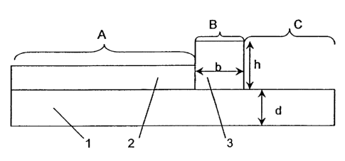
Figures la and 1b diagrammatically show a cross section
through a film according to the invention for a film
capacitor. A carrier film 1 serves as a mechanical
carrier and is electrically insulating and dielectric.
It comprises a plastic, for example a polymer such as
polyethylene, polystyrene, polypropylene, polycarbo-
nate, PET, PEN, cellulose acetate, polyesters, an epoxy
resin, a polysulfone, or another plastic or paper and
is approximately 2-30 ~,.Lm thin. A conductor layer 2
applied thereon is formed as a metal layer or as a
conductive plastic. The conductor layer 2 does not
completely cover one surface of the carrier film 1, so
that there is a free edge. In Figures 1 and 1b, just as
in the following figures, the regions into which the
film surface is subdivided by different coatings are
designated by upper-case letters. Regions of the
surface in which the carrier film 1 is provided with
CA 02409578 2002-10-22
the conductor layer 2 are designated by A, regions in
which it is free of a coating - the free regions - are
designated by C. Situated between the regions A of the
conductor layer 2 and the free regions C is an edge
zone B, where the carrier film is provided with an edge
zone coating 3.
The edge zone coating 3 is produced from a material
having a comparatively low electrical conductivity. Its
width b is between 10 ~m and 5 mm, preferably between
100 ~,m and 2 mm. The thickness h of the edge zone
coating 3 may be less than or greater than the
thickness of the conductor layer 2. Figures la and 1b
each illustrate an example of an edge zone coating
which is thicker and of one which is thinner than the
conductor layer 2.
As- an alternative to the arrangement depicted, the
material of the edge zone coating 3 may also completely
or partly cover the conductor layer 2 in addition to
the edge zone B. Furthermore, the edge zone coating may
also be chosen with a width such that the material of
the edge zone coating completely covers the original
free regions, i.e. that a free region is no longer
present at all at least in regions, but the
conductivity of the edge zone coating is chosen such
that the charge cannot extend over the entire width
within a half-cycle.
Figure 2 illustrates a detail from a film according to
the invention with the region A covered by the
conductor layer, the edge zone B and the free region C
in plan view.
The edge zone coating is intended to be charged
partially, but not completely, during an alternating-
current cycle. What is thus intended to be achieved is
that the potential profile runs more or less
CA 02409578 2002-10-22
_ g _
continuously from the edge of the conductor layer 1
toward the edge, which makes it possible to avoid large
electric field strengths. This means that the RC time
of the edge zone coating must be of the same order of
magnitude as the period T - 1/f (f - frequency) of the
AC voltage. In the case of DC capacitors, the duration
of a voltage transient replaces the period T in the
discussion below. The following thus results
RC = Rs* (b/1) *Ce* (b*1) - R$*Cg*b2 ~ T = 1/f
if Cs is the capacitance per unit area, Rs is the sheet
resistance and 1 is the arbitrarily selected length of
an edge zone coating strip.
The following results from this for the resistivity of
the edge zone coating:
p = h*RS=h/ (f*b2*Cs) - h*d/ (f*b2*~*80)
if d is the thickness of the dielectric carrier film
and E is its dielectric constant. Thus, by inserting
the value of 1/~0 (1013 Vcm/As) and relaxing the
relationship RC - 1/f that is strictly followed above,
a realistic condition results for the edge zone
resistance for a predetermined geometry:
p = [1*1012. . .1*10'6] * (h*d) / (f*b2*E) (SZ*cm) ,
if the frequency f is specified in Hz. The following is
preferably chosen
p = [3*1012. . . 1*1015] * (h*d) / (f*bz*~) (SZ*cm) .
In accordance with a particularly preferred example,
the following holds true
p = [7*101~. . . 1*101'] * (h*d) / (f*bz*E) (SZ*cm) .
CA 02409578 2002-10-22
- 10 -
Analogous relationships apply to the sheet resistance
Rg = p/h, that is to say preferably
Rg = [3*lOla. . .1*1015] *d/ (f*b'*E) (SZ) .
If the abovementioned customary dimensions of the edge
zone coating are taken into account the following
results, for example
p = [4*10'. . . 1*10"] d) / (f*E) (S2*cm)
(d in cm) .
If the film capacitor is operated at 50 Hz, the
following is preferably obtained:
p = [6*1pl°. . .2*101'] * (h*d) / (b2*~) (ECM)~
or:
p = [2*10'. . .2*lOlsl d/~ (S2*cm) .
If the above conditions on the resistivity and the
dimensions of the edge zone coating are met, then the
potential ~ of the fully charged capacitor decreases
(or increases) continuously within the edge zone B as a
function of the distance from the conductor layer, as
is illustrated in Figure 3. In this case, it suffices
if the potential within the edge zone is attenuated to
a fraction, preferably at most a third, of its value
within the conductor layer. This is because, with the
exception of the abovementioned case of a lack of a
free region, it is in no way absolutely necessary to
reduce the potential down to zero within the edge zone.
Figure 4 shows a segmented capacitor film. The
conductor layer 2 has a multiplicity of segments
CA 02409578 2002-10-22
- 12 -
connected by conductor bridges 2.1. Free regions
(region C) extend in between and also at the edge of
the film. Edge zones B according to the invention are
situated between the conductor layer 2 (corresponding
to the region A) and the region C. The figure also
illustrates a region D containing an edge
strengthening.
Figures 5a and 5b show films of a film capacitor with
an internal series circuit. Such an internal series
circuit can be effected in a simple way by a conductor
layer of one film being located opposite two conductor
layers of a second film that are not directly connected
to one another electrically. The figure shows two films
each having a carrier film 1, 1'. The capacitance
formed between a first conductor partial layer 2 of the
first film and a conductor layer 2' of the second film
layer is connected in series with the capacitance
formed between the conductor layer 2' of the second
film and a second conductor partial layer 2" of the
first film. In addition to the edge zone coatings 3, 3'
forming the edge zone, edge strengthenings 4 are also
depicted in the figure. Depending on the construction
of the capacitor (winding, etc.), the two films may
also be segments of a single film.
The edge zone coating can be produced in various ways.
In accordance with a first variant, an alloy having a
reduced electrical conductivity or a semiconductor can
be applied to the carrier film in a targeted manner at
the edges of the conductor layer. This is done using
methods as are already known per se for the application
of strips tenths of millimeters or millimeters wide
(for example from the production of capacitor films, or
else printed circuit boards, etc.), for example with
the aid of a mask, with the aid of photolithographic
methods, etc. A carbon coating or a polymer coating can
also be applied. Finally, the edge zone coating can
CA 02409578 2002-10-22
- 12 -
also be formed by a conductive liquid (oil, ink, etc.)
which, for example, can subsequently also be made
mechanically solid by a gel-forming process.
A further variant provides for the intentional
impairment of conductor properties of the conductor
layer at the edges thereof. This is done, for example,
chemically by targeted exposure of the corresponding
regions B to a reactive atmosphere (oxidation, etc.),
by plasma treatment, etc. However, it can also be
effected mechanically or by heating with a laser.
In accordance with another variant, the uncovered
surface of the carrier film is made conductive, for
example by surface carbonization by laser pyrolysis,
etc.
A current path structure as described in the published
German patent application DE 198 56 457, for example,
may run (not illustrated in the drawings) within the
conductor layer.