Note: Descriptions are shown in the official language in which they were submitted.
CA 02410062 2002-11-20
WO 01/89787 PCT/USO1/16973
MICROFLUIDIC SYSTEMS INCLUDING THREE-DIMENSIONALLY
ARRAYED CHANNEL NETWORKS
Field of Invention
The present invention involves microfluidic network structures, methods for
fabricating microfluidic networlc structures, and methods for using such
structures.
Background of the Invention
The need for complexity in microfluidic systems is increasing rapidly as
sophisticated functions - chemical reactions and analyses, bioassays; high-
throughput
screens, and sensors - are being integrated into single microfluidic devices.
Complex
systems of channels require more complex connectivity than can,be generated in
conventional two-dimensional microfluidic systems having a single level of
channels,
since such typical single-level designs do not allow two channels to cross
without
fluidically connecting. Most methods for fabricating microfluidic channels are
based on
photolithographic procedures, and yield such two-dimensional systems. There
are a
number of more specialized procedures, such as stereolithography (see for
example, K.
Ikuta, K. Hirowatari, T. Ogata, P~oc. IEEE MEMS '94, Oiso, Japan, January 25-
28,
1994, pp. 1-6), laser-chemical three-dimensional writing (see for example,
T.M,.
Bloomstein, D.J. Ehrlich, J. hat. Sci. Tech~ol. B, Vol. 10, pp. 2671-2674,
1992), and
modular assembly (see for example, C. Gonzalez, R.L. Smith, D.G. Howitt, S.D.
Collins,
Sens. Actuators A, Vol. 66, pp. 315-332, 1998), that yield three-dimensional
structures,
but these methods are typically time consuming, difficult to perform, and
expensive, and
are thus not well suited for either prototyping or manufacturing, and are also
not capable
of malting certain types of structures. Better methods for generating complex
three-
dimensional microfluidic systems are needed to accelerate the development of
microfluidic technology. The present invention, in some embodiments, provides
such
improved methods for generating complex three-dimensional microfluidic
systems.
It is known to use a stamp or mold to transfer patterns to a surface of a
substrate
(see for example, R.S. Kane, S. Talcayama, E. Ostuni, D.E. Ingber, G.M.
Whitesides,
Bior~Zater ials, Vol. 20, pp. 2363-2376, 1999; and Y. Xia, G.M. Whitesides,
Ar~ge~~.
Chem. hZt. Ed. E~zgl., Vol. 37, pp. 551-575, 1998; U.S.Pat. No. 5,512,131;
International
Pat. Publication No. WO 97/33737, published 09/18/97). Most conventional soft
CA 02410062 2002-11-20
WO 01/89787 PCT/USO1/16973
-2-
lithographic techniques, for example, microcontact printing (~.CP) (see for
example, C.S.
Chen, M. Mrlcsich, S. Huang, G.M. Whitesides, D.E. Ingber, Science, Vol. 276,
pp.
1425-1428, 1997; A. Bernard, E. Delamarche, H. Schmid, B. Michel, H.R.
Bosshard, H.
Biebuyclc, Langmui~, Vol. 14, pp. 2225-2229, 1998) and micromolding in
capillaries
(MIMIC) (see for example, N.L. Jeon, LS. Choi, B. Xu, G.M. Whitesides, Adv.
Mat.,
Vol. 11, pp. 946-949, 1999; E. Delamarche, A. Bernard, H. Schmid, B Michel, H.
Biebuyclc, Sciefzce, Vol. 276, pp. 779-781, 1997; E. Delamarche, A. Bernard,
H. Schmid,
A. Bietsch, B. Michel, h. Biebuyclc, J. Am. Chenz. Soc., Vol. 120, pp. 500-
508, 1998; A.
Folch, A. Ayon, O. Hurtado, M.A. Schmidt, M. Toner, J. Biomech. Ehg., Vol.
121, pp.
28-34, 1999; A. Folch, M. Toner, Biotech. Prog., Vol. 14, pp. 388-392, 1998),
have been
limited to procedures that pattern one substance at a time, or to relatively
simple,
continuous patterns. These constraints are both topological and practical. The
surface of
a stamp in ~,CP, or of a channel system in MIMIC, is effectively a two-
dimensional
structure. In ~.CP, this two-dimensionality of the stamp limits the types of
patterns that
can be transferred to those comprising a single "color" of ink in the absence
of a way of
selectively "inking" different regions of the stamp with different materials.
Patterning of
multiple "inks" using conventional methods requires multiple steps of
registration and
stamping. In MIMIC, the two-dimensional channel system limits patterning to
relatively
simple, continuous structures or requires multiple patterning steps.
There remains a general need in the art for iW proved methods for forming
patterns on surfaces with soft lithographic techniques, and for providing
techniques able
to pattern onto a surface arbitrary two-dimensional patterns and able to form
complex
patterns comprised of multiple regions, where different regions of the pattern
can
comprise different materials, on a stuface without the need for multiple steps
of
registration or stamping and without the need to selectively "ink" different
regions of the
stamp with different materials. The present invention, in some embodiments,
provides
such improved methods for forming patterns on surfaces with soft lithographic
techniques.
Summary of the Invention
The present invention involves, in certain embodiments, improved microfluidic
systems and procedures for fabricating improved microfluidic systems, which
contain
one or more levels of microfluidic channels. The inventive methods can provide
a
CA 02410062 2002-11-20
WO 01/89787 PCT/USO1/16973
-3-
convenient route to topologically complex and improved microfluidic systems.
The
present invention also, in some embodiments, involves microfluidic systems and
methods for fabricating complex patterns of materials, such as biological
materials and
cells, on surfaces. In such embodiments, the invention involves microfluidic
surface
patterning systems and methods for fabricating complex, discontinuous patterns
on
surfaces that can incorporate or deposit multiple materials onto a surface.
The present
invention, in some embodiments, can provide improved stamps for microcontact
surface
patterning able to pattern onto a surface arbitrary two-dimensional patterns
and able to
pattern multiple substances onto a surface without the need for multiple steps
of
registration or stamping during patterning and without the heed to selectively
"inlc"
different regions of the stamp with different materials.
According to one embodiment of the invention, a microfluidic networlc is
disclosed. The microfluidic network comprises a polymeric structure including
therein
at least a first and a second non-fluidically interconnected fluid flow paths.
At least the.
first flow path comprises a series of interconnected channels within the
polymeric
structure. The series of interconnected channels includes at least one first
channel
disposed within a first level of the structure, at least one second channel
disposed within
a second level of the structure, and at least one connecting channel
fluidically
interconnecting the first channel and the second channel. At least one channel
within the
structure has a cross-sectional dimension not exceeding about 500 ~,m. The
structure
includes at least one channel disposed within the first level of the structure
that is non-
parallel to at least one channel disposed within the second level of the
structure.
In another embodiment of the invention, a microfluidic network is disclosed.
The
microfluidic network comprises an elastomeric structure including therein at
least one
fluid flow path. The flow path comprises a series of interconnected channels
within the
structure. The series of interconnected channels includes at least one first
channel
disposed within a first level of the structure, at least one second channel
disposed within
a second level of the structure, and at least one connecting channel
fluidically
interconnecting the first channel and the second channel. At least one channel
within the
structure has a cross-sectional dimension not exceeding about 500 Vim, and the
structure
includes at least one channel disposed within the first level of the structure
that is non-
parallel to at least one channel disposed within the second level of the
structure.
CA 02410062 2002-11-20
WO 01/89787 PCT/USO1/16973
-4-
In yet another embodiment, a polymeric membrane is disclosed. The polymeric
membrane comprises a first surface including at least one channel disposed
therein, a
second surface including at least one channel disposed therein, and a
polymeric region
intermediate the first surface and the second surface. The intermediate region
includes at
least one connecting channel therethrough fluidically interconnecting the
channel
disposed in the first surface and the channel disposed in the second surface
of the
membrane. At least one channel has a cross-sectional dimension not exceeding
about
500 Vim.
In another embodiment of the invention, a method for forming a microfluidic
network structure is disclosed. The method comprises providing at least one
mold
substrate, forming at least one topological feature on a surface of the mold
substrate to
form a first mold master, contacting the surface with a first hardenable
liquid, hardening
the liquid thereby creating a first molded replica of the surface, removing
the first
molded replica from the first mold master, and assembling the first molded
replica into a
structure comprising a microfluidic network. The assembled microfluidic
network
structure has at least one fluid flow path comprising a series of
interconnected channels
within the structure. The series of interconnected channels includes at least
one first
channel disposed within a first level of the structure, at least one second
channel
disposed within a second level of the structure, and at least one connecting
channel
fluidically interconnecting the first channel and the second channel. At least
one of the
channels within the structure leas a cross-sectional dimension not exceeding
about 500
Vim. The structure includes at least one channel disposed within the first
level of the
structure that is non-parallel to at least one channel disposed within the
second level of
the structure.
In yet another embodiment, a method for forming a molded structure is
disclosed.
The method comprises providing at least one mold substrate and forming at
least one
two-level topological feature having at least one lateral dimension not
exceeding 500 ~.m
on a surface of the substrate to form a mold master. The two-level topological
feature is
characterized by a first portion having a first depth or height with respect
to a region of
the surface adjacent to the feature, and a second portion integrally connected
with the
first portion having a second depth or height with respect to the region of
the surface
adjacent to the feature that is greater than the first depth or height. The
method further
comprises contacting the surface with a hardenable liquid, hardening the
liquid thereby
CA 02410062 2002-11-20
WO 01/89787 PCT/USO1/16973
-5-
creating a molded replica of the surface, and removing the molded replica from
the mold
master.
In another embodiment of the invention, a method for forming topological
features on a surface of a material is disclosed. The method comprises
exposing portions
of a surface of a first layer of photoresist to radiation in a first pattern,
coating the surface
of the first layer of photoresist with a second layer of photoresist, exposing
portions of a
surface of the second layer of photoresist to radiation in a second pattern
different from
the first pattern, and developing the first and second photoresist layers with
a developing
agent. The developing step yields a positive relief pattern in photoresist
that includes at
least one two-level topological feature having at least one cross-sectional
dimension not
exceeding 500 ~.m. The two-level topological feature is characterized by a
first portion
having a first height with respect to the surface of the material and a second
portion,
integrally connected to the first portion, having a second height with respect
to the
surface of the material.
In yet another embodiment, a method for forming a molded structure is
disclosed.
The method involves providing a first mold master having a surface formed of
an
elastomeric material and including at least one topological feature with at
least one cross-
sectional dimension not exceeding about 500 ~.m thereon. The method further
comprises
providing a second mold master having a surface including at least one
topological
feature with at least one cross-sectional dimension not exceeding about 500 ~m
thereon.
The method further comprises placing a hardenable liquid in contact with the
surface of
at least one of the first and second mold master, bringing the surface of the
first mold
master into at least partial contact with the surface of the second mold
master, hardening
the liquid thereby creating a molded replica of the surface of the first mold
master and
the surface of the second mold master, and removing the molded replica from at
least one
of the mold masters.
In another embodiment of the invention, a method for forming a molded
structure
is disclosed. The method involves providing a first mold master having a
surface
including at least a first topological feature with at least one cross-
sectional dimension
not exceeding about 500 ~m thereon and at least a second topological feature
comprising
a first alignment element. The method further comprises providing a second
mold
master having a surface including at least a first topological feature with at
least one
cross-sectional dimension not exceeding about 500 ~.m thereon and at least a
second
CA 02410062 2002-11-20
WO 01/89787 PCT/USO1/16973
-6-
topological feature comprising a second alignment element having a shape that
is
mateable to the shape of the first alignment element. The method further
comprises
placing a hardenable liquid in contact with the surface of at least one of the
first and
second mold master, bringing the surface of the first mold master into at
least partial
contact with the surface of the second mold master, aligning the first
topological features
of the first and second mold masters with respect to each other by adjusting a
position of
the first mold master with respect to a position of the second mold master
until the first
alignment element matingly engages and interdigitates with the second
alignment
element, hardening the liquid thereby creating a molded replica of the surface
of the first
mold master and the surface of the second mold master, and removing the molded
replica
from at least one of the mold masters.
In yet another embodiment of the invention, a method for aligning and sealing
together surfaces is disclosed. The method comprises disposing two surfaces,
at least
one of which is oxidized, adjacent to each other such that they are separated
from each
other by a continuous layer of a liquid that is essentially non-reactive with
the surfaces,
aligning the surfaces with respect to each other, and removing the liquid from
between
the surfaces, thereby sealing the surfaces together via a chemical reaction
between the
surfaces.
In another embodiment of the invention, a method for molding an article is
disclosed. The method comprises providing a first mold master having a surface
with a
first set of surface properties and providing a second mold master having a
surface with a
second set of surface properties. At least one of the first and second mold
masters has a
surface including at least one topological feature with at least one cross-
sectional
dimension not exceeding about 500 ~m thereon. The method further comprises
placing a
hardenable liquid in contact with the surface of at least one of the first and
second mold
masters, bringing the surface of the first mold master into at least partial
contact with the
surface of the second mold master, hardening the liquid thereby creating a
molded
replica of the surface of the first mold master and the surface of the second
mold master,
separating the mold masters from each other, and removing the molded replica
from the
surface of the first mold master while leaving the molded replica in contact
with and
supported by the surface of the second mold master.
In yet another embodiment, a microfluidic network is disclosed. The
microfluidic network comprises a polymeric structure including therein at
least a first
CA 02410062 2002-11-20
WO 01/89787 PCT/USO1/16973
7_
and a second non-fluidically interconnected fluid flow paths. The first flow
path
comprises at least two non-colinear interconnected channels disposed within a
first
pla~ze, and the second flow path comprises at least one channel disposed
within a second
plane that is non-parallel with the first plane. At least one chamiel within
the structure
has a cross-sectional dimension not exceeding about 500 Vim.
In another embodiment of the invention, a microfluidic network is disclosed.
The
microfluidic network comprises a polymeric structure including therein at
least one fluid
flow path. The fluid flow path is formed of at least one channel and has a
longitudinal
axis defined by the direction of bulls fluid flow within the flow path. The
longitudinal
axis of the flow path is not disposed within any single plane.
In another embodiment of the invention, a method of patterning a material
surface is disclosed. The method comprises providing a stamp having a
structure
including at least one flow path comprising a series of interconnected
channels within the
structure. The series of interconnected channels includes at least one first
channel
disposed within an interior region of the structure, at least one second
channel disposed
within a stamping surface of the structure defining a first pattern therein,
and at least one
connecting channel fluidically interconnecting the first channel and the
second channel.
The method further comprises contacting the stamping surface with a portion of
the
material surface, and, while maintaining the stamping surface in contact with
the portion
of the material surface, at least partially filling the flow path with a fluid
so that at least a
portion of the fluid contacts the material surface.
In yet another embodiment, a method of patterning a material surface is
disclosed. The method comprises providing a stamp having a structure including
at least
two non-fluidically interconnected flow paths therein including a first fluid
flow path
defining a first pattern of channels disposed within a stamping surface of the
structure
and a second fluid flow path defining a second pattern of channels disposed
within the
stamping surface of the structure. Each of the first and second patterns of
channels is
non-continuous, and the channels defining the first pattern are non-
intersecting with the
channels defining the second pattern. The method further comprises contacting
the
stamping surface with a portion of the material surface, while maintaining the
stamping
surface in contact with the portion of the material surface, at least
partially filling the first
flow path with a first fluid so that at least a portion of the first fluid
contacts the material
surface and at least partially filling the second flow path with a second
fluid so that at
CA 02410062 2002-11-20
WO 01/89787 PCT/USO1/16973
_g_
least a portion of the second fluid contacts the material surface, and
removing the
stamping surface to provide a pattern on the material surface according to the
first
pattern, which is formed by contact of the material surface with the first
fluid, and
according to the second pattern, which is formed by contact of the material
surface with
the second fluid.
In another embodiment, a method of patterning a material surface is disclosed.
the method involves providing a stamp having a structure including at least
one non-
linear fluid flow path therein in fluid commuucation with a stamping surface
of the
structure. The method fiu~ther involves contacting the stamping surface with a
portion of
the material surface and, while maintaining the stamping surface in contact
with the
portion of the material surface, at least partially filling the flow path with
a fluid so that
at least a portion of the fluid contacts the material surface.
Other advantages, novel features, and objects of the invention will become
apparent from the following detailed description of the invention when
considered in
conjunction with the accompanying drawings, which are schematic and which are
not
intended to be drawn to scale. In the figures, each identical or nearly
identical
component that is illustrated in various figures is represented by a single
numeral. For
purposes of clarity, not every component is labeled in every figure, nor is
every
component of each embodiment of the invention shown where illustration is not
necessary to allow those of ordinary slcill in the art to understand the
invention.
Brief Description of the Drawings
FIG. la is a perspective view of a schematic illustration of a microfluidic
network
structure having a series of interconnected channels arranged in a
"baslcetweave"
configuration;
FIG. 1b is a two-dimensional projection of the microfluidic network structure
of
FIG. 1 a;
FIG. 2a is a perspective view of a schematic illustration of a second
embodiment
of a microfluidic network structure;
FIG. 2b is a two-dimensional projection of the microfluidic network structure
of
FIG. 2a;
FIG. 3a is a perspective view of a schematic illustration of a third
embodiment of
a microfluidic network structure;
CA 02410062 2002-11-20
WO 01/89787 PCT/USO1/16973
-9-
FIG. 3b is a two-dimensional projection of the microfluidic network structure
of
FIG. 3 a;
FIG. 4a is a perspective view of a schematic illustration of a five-level
microfluidic network comprising a centrally disposed straight channel
surrounded by a
coiled fluid flow path;
FIG. 4b is a two-dimensional projection of the microfluidic network structure
of
FIG. 4a;
FIGS. Sa-Sc are schematic illustrations of one embodiment of the fabrication
method for forming a microfluidic network structure according to one
embodiment of the
invention;
FIGS. 6a-6c are schematic illustrations of one embodiment of a self aligning
method provided by the invention;
FIG. 6d is a schematic illustration of a replica molded layer of a
microfluidic
network having a perimetric shape for use in one embodiment of a self aligning
method
according to the invention;
FIG. 7 is a schematic illustration of a second embodiment of a microfluidic
network fabrication method according to the invention;
FIG. 8 is a schematic illustration of a method for forming a two-level
topological
feature on a surface of the substrate by photolithography provided according
to the
invention;
FIGs. 9a-9b are schematic illustrations of a third embodiment for forming a
microfluidic network structure according to the invention;
FIG. 9c is a series of schematic, cross-sectional illustrations of a
modification of
the third embodiment for forming the microfluidic networlc structure of FIGs.
9a-9b.
FIG. 10 is a schematic illustration of a method for forming a five-level
microfluidic network structure including a straight channel surrounded by a
coiled series
of interconnected channels;
FIG. 11 is a schematic illustration of a pattern on a material surface formed
with
a microfluidic stamp provided according to the invention;
FIG. 12a is a perspective view of a schematic illustration of a lower and an
upper
mold master for forming a baslcetweave microfluidic networle structure
provided by the
invention;
CA 02410062 2002-11-20
WO 01/89787 PCT/USO1/16973
-10-
FIGS. 12b-12c provide photocopies of photomicrographs of a microfluidic
networlc characterized by a network of channels arranged in a baslcetweave
configuration
in accordance with one embodiment of the present invention;
FIG. 12d is a photocopy of an SEM image of a micromolded structure produced
according to one embodiment of the invention;
FIG. 13 is a photocopy of a photomicrograph of a microfluidic network
comprising a straight channel surrounded by a coiled fluid flow path
comprising a series
of interconnected channels, according to one embodiment of the invention;
FIG. 14a is a schematic illustration of a microfluidic stamping process
according
to one embodiment of the invention;
FIG. 14b is a schematic illustration of the fluid flow path layout of the
microfluidic stamp illustrated in FIG. 14a;
FIG. 14c is a photocopy of a photomicrograph of a patterned surface produced
using the microfluidic stamp illustrated in FIG. 14a;
FIG. 15a is a schematic illustration of the layout of fluid flow paths in one
embodiment of a microfluidic stamp provided according to the invention;
FIG. 15b is a photocopy of photomicrograph of a stamped pattern on a material
surface produced using a microfluidic stamp having the microfluidic network
structure
illustrated in FIG. 15a;
FIG. 16a is a schematic illustration of the layout of fluid flow paths in one
embodiment of a microfluidic stamp provided according to the invention;
FIGs. 16b-16d are photocopies of photomicrographs of patterned cells on a
material surface deposited using a microfluidic stamp having the microfluidic
network
configuration illustrated in FIG. 16a;
FIG. 17a is a schematic illustration of the layout of fluid flow paths in one
embodiment of a microfluidic stamp provided according to the invention; and
FIGs. 17b-17e are photocopies of photomicrographs of patterned cells on a
material surface deposited using a microfluidic stamp having the microfluidic
network
configuration illustrated in FIG. 17a.
Detailed Description
The present invention is directed to fabrication methods for producing three-
dimensional microfluidic network structures, polymeric microfluidic network
structures
CA 02410062 2002-11-20
WO 01/89787 PCT/USO1/16973
-11-
having a three-dimensional array of channels included therein, and various
uses for the
microfluidic networks, for example as a template for forming and depositing
complex
patterns on substrates. A "three-dimensional microfluidic networlc," "three-
dimensional
microfluidic network structure," or "three-dimensional microfluidic stamp" as
used
herein refers to a structure capable of containing a fluid and/or providing
fluid flow
therethrough, which includes at least three channels therein, and may contain
many
more; furthermore, the structure includes at least three channels that are
arranged with
respect to each other such that there exists no plane, or curved planar
surface, which
contains disposed therein the longitudinal axes of the three channels. The
microfluidic
networks provided according to the invention, because of their three-
dimensionality of
structure, are able, for example, to provide channels within the structure
having
longitudinal axes (defined as the axial centerline of the channel aligned
parallel to the
direction of bulls fluid flow within the channel) aligned along each of the x,
y, and z
directional components of space. The ability to produce microfluidic
structures having
channels arranged in a three-dimensional networlc enables the systems provided
according to the invention to include therein a plurality of channels
providing one or
more independent fluid flow paths, where the channels and flow paths can be
arrayed in
arbitrarily complex geometric networlcs since the channels of the structures
have the
capability of crossing over and/or under each other within the structure.
One way to analogize the capabilities of the microfluidic networlcs, and
methods
for producing the microfluidic networlcs, according to the invention, is to
compare the
channel systems of the microfluidic networlcs to a lcnot in three-dimensional
space. The
microfluidic networks provided according to the invention have the ability to
fabricate
the physical realization of knots, and thus can include channel systems of
arbitrary
topological complexity. In mathematical terms, a knot is a closed, non-
intersecting,
curved line in three dimensions. Knots are typically described in mathematics
in terms
by their projections onto a plane. For non trivial knots, these projections
contain "double
points", which are points where the projected curve crosses itself. A lcnot
can always be
slightly perturbed in three dimensions so that, in projection, it has no
triple or higher
order points: that is, points where the projected curve crosses itself three
or more times.
Hence, lcnots can be described completely by giving such a two-dimensional
projection,
together with information about which piece of the curve crosses over or under
the
another piece at each double point.
CA 02410062 2002-11-20
WO 01/89787 PCT/USO1/16973
-12-
The microfluidic networks provided according to the invention, because of
their
three-dimensional channel network structure, are able to provide a physical
realization of
the above-mentioned double point. In other words, the structures enable one
channel,
comprising a flow path or a segment of a flow path, to cross over or under
another
channel providing another flow path, a segment of another flow path, or
providing
another segment of the same flow path. Thus, the inventive microfluidic
networlcs can
provide a physical realization of essentially any topological knot system.
Likewise, the
inventive networks can provide a physical realization of essentially any
arrangement of
interlinlced knots and of arbitrarily complex three-dimensional networks of
interconnected channels Whose projections onto a plane or surface, as
explained in more
detail below, can contain any arbitrary number of crossings. As shown and
explained in
more detail below, in order for the inventive microfluidic networks to avoid
intersection
of channels at their points of crossing in the planar projection, there
typically are
provided at least three identifiable "levels" within the structure: a "lower"
level that
contains a channel disposed therein that crosses "under" an "upper" level that
contains
disposed therein a channel that crosses "over" the channel contained in the
bottom level,
and an intermediate level that isolates the channels of the lower and upper
levels and
contains connecting channels penetrating therethrough that fluidically connect
the
channels in the lower level and the channels on the upper level in order to
form a fluid
flow path comprised of a series of interconnected channels. It should be
understood that
the terms "lower" and "upper" in the present context are intended to suggest
only the
relative positions of the various levels of the structure and are not meant to
imply any
particular orientation of the structure in space. For example the structure
can be flipped ,
rotated in space, etc. so that the "lower" level is positioned above the
"upper" level or the
levels can be positioned side by side, etc. In yet other embodiments involving
flexible
structures, the structL~re can be twisted or bent thereby deforming planar
levels into
curved surfaces in space such that the "upper" and "lower" levels of the
structure may be
positioned differently with respect to each other at different locations in
the overall
structure. In order to produce microfluidic networks with arbitrarily complex
channel
networlcs, no additional levels are typically needed because triple, or higher
order points
in the projection are not necessary to allow the channels within the structure
to cross over
or under each other and thus cross each other in space without physical
intersection of
the "crossing" channels within the structure.
CA 02410062 2002-11-20
WO 01/89787 PCT/USO1/16973
-13-
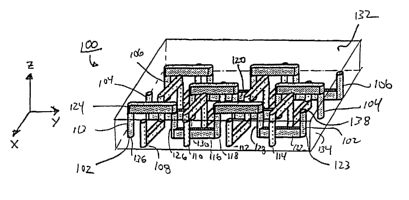
FIG. 1 a illustrates one exemplary embodiment of an essentially infinite
number
of microfluidic network structures that can be produced according to the
invention.
Microfluidic network structure 100 includes a series of interconnected
channels
providing seven non-fluidically interconnected fluid flow paths. The channels
are
arranged in a "basket weave" arrangement. Channel system 100, as illustrated,
includes
three non-fluidically interconnected fluid flow paths, 102, 104, and 106
arrayed within
planes parallel to the y-z coordinate plane, and four non-fluidically
interconnected flow
paths 108, 110, 112, and 114 arrayed within planes parallel to the x-z
coordinate plane.
Each fluid flow path of the structure comprises a series of interconnected
channels (e.g.
fluid flow path 102 comprises interconnected channels 113, 124, 126, 116, 118,
120,
128, 122 and 123 within structure 100).
Flow path 102, for example, includes two channels 116 and 122 disposed within
the first, lower level of structure 100 and two channels 120 and 124 disposed
within the
second, upper level of the structure. Flow path 102 also includes a number of
connecting
channels, e.g. 118, 126, and 128 traversing a third, intemnediate level of the
structure and
interconnecting channels contained in the first, lower level and second, upper
level of the
structure. The microfluidic networlc provided by structure 100 is truly three-
dimensional
because it cannot be produced by a two-dimensional structure comprising a
series of
interconnected chamiels disposed within a single plane or any stack or array
of such
structures. In other words, networlc 100 includes channels disposed within the
first,
lower level of the structure that are non-parallel to channels,disposed within
the second,
upper level of the structure (e.g. channel 116 of fluid flow path 102 and
channel 130 of
fluid flow path 110). Another way to describe the three-dimensionality of
network 100,
and distinguish the networlc from those realizable in two-dimensional system,
is to point
out, that, for example, flow path 102 comprises a series of non-colineax
interconnected
channels disposed within a first plane of the structure, which is parallel to
the y-z
coordinate plane, and a second fluid flow path, for example, fluid flow path
108, is
disposed within a second plane (parallel to the x-z coordinate plane as shown)
that is not
parallel with the first plane. Yet another way in which the microfluidic
networks
provided according to the invention differ from those realizable with two-
dimensional
systems is that the inventive microfluidic systems can include a fluid flow
path therein
having a longiW dinal axis, defining a direction of bulk fluid flow within the
flow path,
CA 02410062 2002-11-20
WO 01/89787 PCT/USO1/16973
-14-
that is not disposed within any single plane in space, nor is disposed within
any a surface
that is parallel to any surface (such as surface 132 or 134) of the
microfluidic structure.
A "level" of a structure, as used herein, refers to a plane or curved surface
within
the structure, typically parallel to a top surface and a bottom surface of the
structure,
which can have a channel or series of channels disposed therein and/or
penetrating
therethrough. It should be understood that in the discussion and figures
illustrated
below, the microfluidic network structures are generally shown as having
planar surfaces
(e.g. surfaces 132 and 134), such that the levels within the structure are
planar; however,
many of the structures, as described in more detail below, are fabricated from
flexible
and/or elastomeric materials that are capable of being bent twisted, or
distorted from the
illustrated planar configurations. For such embodiments, the "levels" within
the
structure will comprise curved surfaces that are parallel to the distorted
planar surfaces of
the structure, and any discussion herein with regard to "levels" of the
structures should
be understood to encompass such curved surfaces as well as the planar surfaces
illustrated. "Parallel," when used in the context of comparing the topology of
two
surfaces in space, has its common mathematical meaning referring to the two
surfaces
being everywhere spaced apart from each other equidistantly.
"Non-fluidically interconnected" fluid flow paths, as used herein, refers to
fluid
flow paths each comprising one channel or multiple, fluidically interconnected
channels,
where the channels of different flow paths do not intersect and are physically
isolated
from each other within the structure so that they can not communicate fluid
between each
other through bulls mixing of fluid streams. A "fluid flow path" as used
herein refers to
one channel or a series of two or more interconnected channels providing a
space within
the microfluidic structure able to contain fluid or through which fluid can
continuously
flow. Each fluid flow path of the structure includes at least one opening
thereto able to
be placed in fluid communication with the environment external to the
microfluidic
structure and some preferred embodiments of fluid flow paths include at least
two
openings able to be placed in fluid conununcation with the environment
external to the
microfluidic structure, thus providing an inlet and an outlet. A "channel" as
used herein
refers to a flow path or continuous segment of a flow path, which is disposed
within one
or more levels of the microfluidic network structure and/or penetrates through
one or
more levels of the microfluidic networlc structure. "Interconnected channels,"
as used
herein, refers to two or more channels within the structure that are able to
communicate
CA 02410062 2002-11-20
WO 01/89787 PCT/USO1/16973
-15-
fluid between and through each other. A "non-linear" flow path and/or channel,
as used
herein, refers to such flow path or channel having a longitudinal axis that
deviates from a
straight line along its length by more than an amount equal to the minimum
cross-
sectional dimension of the channel or flow path. A "longitudinal axis" of a
channel or
flow path as used herein refers to an axis disposed along the entire length of
such
channel or flow path, which is coextensive with and defined by the geometric
centerline
of the direction of any bulb fluid which would flow through the channel or
flow path
should such channel or flow path be configured for fluid flow therethrough.
For
example, a linear or "straight" channel would tend to have a longitudinal axis
that is
essentially linear, while a fluid flow path comprising a series of such
straight channels
that are fluidically interconnected can have a longitudinal axis, comprising
the
interconnected longitudinal axes of the individual interconnected channels
forming the
fluid flow path, which is "non-linear." A channel which is "disposed within,"
"disposed in," "contained within," or "contained in" a level or multiple
levels of the
structure refers herein to such channel having a longitudinal axis that is
coplanar with or,
in the case of a level defined by a curved surface, is lying along a contour
of the surface,
of the levels) in which it is disposed or contained. A channel that
"penetrates,"
"penetrates through," or "traverses" a level or multiple levels of the
structure refers
herein to such channel having a longitudinal axis that is non-coplanar with
or, in the case
of a level defined by a curved surface, is not lying along a contour of the
surface of the
levels) such that the longitudinal axis of such channel is non-parallel with
any line that
can be disposed within the level.
Fluid flow path 102 of microfluidic network 100 cormnunicates with the
external
environment through an inlet opening 136 in fluid communication with bottom
surface
134 and an outlet opening 138 in fluid cormnunication with upper surface 132.
The
other fluid flow paths of the network have similar inlet and outlet openings,
as
illustrated.
The channels of the microfluidic networks provided according to the invention
have at least one cross-sectional dimension that does not exceed about 500
~,m, in other
embodiments does not exceed about 250 ~,m, in yet other embodiments does not
exceed
about 100 Vim, in other embodiments does not exceed about 50 p,m, and in yet
other
embodiments does not exceed about 20 ~.m. A "cross-sectional dimension," when
used
in the above context, refers to the smallest cross-sectional dimension for a
cross-section
CA 02410062 2002-11-20
WO 01/89787 PCT/USO1/16973
-16-
of a channel talcen perpendicular to the longitudinal axis of the channel.
While the
channels of network 100 have cross-sectional dimensions that are essentially
equal to
each other, in other embodiments, the channels can have unequal cross-
sectional
dimensions, and some channels can have depths within the structure
sufficiently great so
that they are disposed in two or all three levels of the structure, instead of
being disposed
in only a single level, as illustrated. In addition, while in network 100 the
channels are
straight and linear, in other embodiments the channels can be curved within
the levels)
in which they are disposed.
The double points formed where the channels of the fluid flow paths of network
100 cross over each other are more clearly seen in the two-dimensional
perpendicular
projection shown in FIG. 1b. FIG. 1b shows microfluidic network 100 as
projected onto
the y-x plane as viewed in the negative z-axis direction. Crossover double
point 140, for
example, represents the double point defining the cross over of channel 130 of
fluid flow
path 110 and channel 116 of fluid flow path 102. In general, microfluidic
networks
provided according to the invention having fluid flow paths including channels
that
"cross over" each other refers to structures including channel networlcs
wherein a
perpendicular projection of the channels onto a surface defining a level of
the structure,
in which either of the channels are disposed, at least partially overlap each
other. A
"perpendicular projection" refers to a projection in a direction that is
perpendicular or
normal to the surface being proj ected upon. "At least partially overlap" or
"at least
partially overlapping," as used herein when referring to projections of
channels which
cross over each other, refers to the two-dimensional projection of the
channels
intersecting each other, as shown by point 140 in FIG. 1b, or, if, for
example, the
channels are arranged in a parallel direction with respect to each other
within the network
structure, to their being at least partially superimposed upon each other in
the two-
dimensional projection.
While the three-dimensional microfluidic network structures described herein
could potentially be fabricated via conventional photolithography,
microassembly, or
micromachining methods, for example, stereolithography methods, laser chemical
three-
dimensional writing methods, or modulax assembly methods, as described in more
detail
below, the invention also provides improved fabrication methods for producing
the
inventive structures involving replica molding techniques for producing
individual layers
which comprise one or more of the levels of the structures, as discussed
above. As
CA 02410062 2002-11-20
WO 01/89787 PCT/USO1/16973
17-
described in more detail below, such layers are preferably molded utilizing
mold masters
having various features on their surfaces) for producing channels of the
structure. In
some preferred embodiments, the features are formed via a photolithography
method, or
can themselves comprise a molded replica of such a surface.
The microfluidic network structures produced by the inventive methods
described
herein can potentially be formed from any material comprising a solid material
that
comprises a solidified form of a hardenable liquid, and, in some embodiments,
the
structures can be injection molded or cast molded. As will be described in
more detail
below, preferred hardenable liquids comprise polymers or precursors of
polymers, which
harden upon, or can be induced to harden during, molding to produce polymeric
structures. For reasons described in more detail below, particularly preferred
polymeric
materials for forming the microfluidic networks according to the invention
comprise
elastomeric materials.
For structures produced according to the preferred methods described herein,
the
microfluidic networks provided according to the invention will typically be
comprised of
at least one discrete layer of polymeric material, and other embodiments will
be
comprised of at least two discrete layers of polymeric material, and in yet
other
embodiments will be comprised of three or more discrete layers of polymeric
material.
A "discrete layer" of material as used herein refers to a separately formed
subcomponent
structure of the overall microfluidic structure, which layer can comprise
and/or contain
one, two, or three, or more levels of the overall channel network of the
microfluidic
structure. As described and illustrated in more detail below, the discrete
layers of the
structure can be stacked together to form a three-dimensional network, or
multiple three-
dimensional networks, if desired, and can also be, in some embodiments, placed
between
one or more support layers or substrate layers in order to enclose and
fluidically seal
channels of the lower and upper levels of the microfluidic structure.
As described in more detail below, the methods for producing microfluidic
network structures provided by the invention can, in some embodiments, produce
discrete layers comprising a single level of the overall structure, wherein
the three-
dimensional network structure is formed by forming a first layer including a
series of
channels disposed therein, forming a second layer including a second series of
channels
disposed therein, and forming a third layer having connecting channels
traversing the
layer, and subsequently stacking the third layer between above-mentioned first
and
CA 02410062 2002-11-20
WO 01/89787 PCT/USO1/16973
_ 18-
second layers and aligning the layers with respect to each other to achieve
the overall
desired three-dimensional network structure. In another embodiment, the
microfluidic
network structure includes two channel-containing layers: a first discrete
layer containing
both a first level, including a series of channels disposed therein, and a
third,
intermediate level of the structure including the connecting channels
traversing the level;
and a second discrete layer including the second level of the structure,
having a second
series of channels disposed therein. In such a method the first discrete layer
and the
second discrete layer are stacked and aligned with respect to each other to
produce the
overall desired three-dimensional microfluidic networlc structure. And in yet
a third
embodiment, all three levels of the microfluidic networlc structure can be
produced in a
single discrete layer, the layer comprising a three-level microfluidic
membrane structure.
FIGS. 2a and 2b illustrate a microfluidic structure 150 having an alternative
three-
dimensional arrangement of channels therein. Microfluidic network 150 includes
two
non-fluidically intercormected flow paths 152 and 154. Fluid flow path 152
comprises a
series of intercormected channels 156, 158, 160, 162 and 164, which are non-
linear and
which define a plane parallel to the y-z coordinate plane. Channels 156 and
164 are
disposed within a first, lower level of the structure, and channel 160 is
disposed within a
second, upper level of the structure. Connecting channel 158 traverses a
third,
intermediate level of the structure from the first, lower level to the second,
upper level
and fluidically interconnects channel 156 to channel 160. Similarly,
connecting channel
162 traverses the third, intermediate level of the structure connecting
channel 164 and
channel 160. Flow path 152 is connected in fluid communication with the
external
environment via inlet opening 168 in side wall 170 an outlet opening 172 in
side wall
174. Fluid flow path 154 comprises a single channel 176 disposed within the
first, lower
level of the structure, and is interconnected to the environment via inlet
opening 178 in
side wall 180 an outlet opening 182 in side wall 190. The perpendicular
projection of the
microfluidic channel network, onto the first, lower level of the structure is
illustrated in
FIG. 2b. FIG. 2b shows double point 192 where channel 160 of fluid flow path
152
crosses over channel 176 of fluid flow path 154.
FIGs. 3a and 3b illustrate yet another simple microfluidic network provided
according to the invention but not achievable with a conventional two-
dimensional
microfluidic network structure. Microfluidic network 200 includes a single
fluid flow
path 202. Fluid flow path 202 is comprised of a first channel 204 disposed
within a first,
CA 02410062 2002-11-20
WO 01/89787 PCT/USO1/16973
-19-
lower level of the structure; a second channel 206 disposed within a second,
upper level
of the structure; and a connecting channel 208 traversing a third,
intermediate level of the
structure and fluidically interconnecting channels 204 and 206. Channel 204
disposed
within the first level of the structure and channel 206 disposed within the
second level of
the structure are non parallel to each other and, in the illustrated
embodiment, happen to
be perpendicular to each other. FIG. 3b illustrates the perpendicular
projection of
microfluidic network 200 onto the first, lower level structure along the
negative z-axis
direction. As illustrated, microfluidic network 200 does not include any
crossover points
in the projection.
As previously discussed, a microfluidic network need only include three levels
therein (a first and a second level including channels disposed therein such
that their
longitudinal axes are coplanar with a surface defining the level and a third
intermediate
level having one or more connecting channels passing therethrough fluidically
connecting the channels of the first level and the second level) in order to
provide any
arbitrarily complex network of channels that pass over and under one another.
However,
certain potentially desirable geometric configurations of channels may require
more than
the three levels contained within the structures discussed and illustrated
above. For
example, if it is desired to produce a microfluidic networlc having channels
disposed
within three or more non-coplanar levels of the structure, additional levels
are needed. In
general, the number of levels required for microfluidic structures produced
according to
the invention required to produce n levels, each level having channels
disposed therein
such that their longitudinal axis are coplanar with the level, requires a
total of 2n-1 total
levels in the structure. Thus, for the previously illustrated embodiments
having two
levels therein in which channels are disposed, each structure requires a total
of three
levels to form the overall networlc structure (an upper and lower level in
which the
channels are disposed and an intermediate level through which the connecting
channels
pass).
FIGS. 4a and 4b illustrate one embodiment of a microfluidic structure,
producible
according to the methods of the invention described below, including therein
three levels
having channels disposed therein such that their longitudinal axes are
coplanar with each
of the levels, and a total of five levels overall. Structure 220 includes a
microfluidic
network comprising a fluid flow path 222 arranged as a coil surrounding a
second fluid
flow path 224. Such an arrangement may be especially useful for particular
microfluidic
CA 02410062 2002-11-20
WO 01/89787 PCT/USO1/16973
-20-
applications involving, for example, heat transfer or mass transfer between
components
contained within fluid flow paths 222 and 224, or for embodiments where
electrical,
magnetic, optical or other environmental interaction between materials in the
respective
flow paths is desired.
The first, lower level of structure 220 includes disposed therein channels
226,
228, 230, and 232 of coil flow path 222. The second level from the bottom of
structure
220 includes disposed therethrough the lowermost region 234 of connecting
channels
236, 238, 240, 242, 244, 246, and 248 of fluid flow path 222. The third level
from the
bottom of structure 220 includes channel 250 of fluid flow path 224 disposed
therein and
also includes intermediate region 251 of the connecting channels. The fourth
level from
the bottom of structure 220 includes, traversing therethrough, upper regions
252 of the
connecting channels, and the uppermost level of structure 220 includes
disposed therein
channels 254, 256, 258 and 260 of flow path 222.
FIG. 4b illustrates the perpendicular projection of microfluidic network 220
onto
a surface coplanar with the first, lowermost level of the structure that is
parallel to the y-
x coordinate plane, as viewed in the negative z direction. As illustrated,
structure 220
includes 8 double point crossovers 264, 266, 267, 268, 269, 270, 272, and 274
where
either flow path 224 crosses over a channel of flow path 222 (e.g. crossover
points 264,
267, 269, and 272), or where channel 250 of flow path 224 crosses under a
channel of
fluid flow path 222, (for example, crossover point 266, 268, 270, and 274.) It
should be
evident that the five level structure illustrated by structure 220, in
alternative
embodiments, can have flow paths therein comprising a series of interconnected
channels arranged so as to yield higher order crossover points than the double
points
illustrated. For example, in other embodiments, a five level structure can
have channels
disposed therein including triple point crossovers wherein a perpendicular
projection
onto a surface coplanar with a level of the structure includes points where
three levels of
channels intersect (i.e., where a channel disposed in the lowermost level, a
channel
disposed in the third, intermediate level, and a channel disposed in the
uppermost level
overlap andlor intersect each other in the two-dimensional projection).
As discussed above, the present invention also provides a variety of methods
providing relatively simple and low cost fabrication techniques for producing
the
inventive microfluidic structures described herein. The preferred methods
provided
according to the invention and described below are based upon utilizing a
hardenable
CA 02410062 2002-11-20
WO 01/89787 PCT/USO1/16973
-21 -
liquid to create replica molded structures that comprise, or are assembled
with other
replica molded structures to form, the three-dimensional microfluidic network
structures
provided by the invention.
FIGS. Sa-Sc illustrate a first embodiment of a method for forming the
inventive
microfluidic structures by utilizing a replica molding process provided by the
invention.
The method illustrated by FIGS. Sa-Sc involves forming a number of replica
molded
layers from a hardenable liquid, each of which structures comprises a single
level of the
overall microfluidic network. Following the fabrication of each of the replica
molded
structures comprising layers of the overall microfluidic network structure,
the layers are
staclced upon each other, aligned with respect to each other so that the
respective molded
features in the layers create the desired and predetermined microfluidic
networlc pattern,
and, optionally, the layers can be permanently sealed to each other and/or to
one or more
substrate layers, which substrate layers do not comprise a level of the
overall
microfluidic structure, in order to yield a finished microfluidic network
structure having
a desired configuration.
Step 1 as illustrated in FIG. 5a involves forming a first layer of the
structure
comprising, for example, a first, lower level of the microfluidic networlc. Of
course, in
other embodiments, layers comprising an upper or intermediate level of the
structure can
be molded before or at the same time a lower layer is molded. In general, the
order of
the molding steps is not particularly critical and the various layers of the
overall structure
can be molded in any order that is desired or convenient. In the illustrated
embodiment,
a lower mold master 300 is provided having a series of topological features
302
protruding from an upper surface 304 of the lower mold master. A second mold
master
306 having a flat, featureless surface 308 facing surface 304 of mold master
300 is
provided and placed in contact with an upper surface of topological features
302 of mold
master 304. Disposed between mold masters 304 and 306 is a layer of hardenable
liquid
310, which upon solidification forms a replica molded layer including therein
a plurality
of channels, formed by topological features 302 of mold master 304, which,
channels, in
preferred embodiments, pass completely through the thiclcness of the entire
layer of
liquid 310, upon hardening, thus forming a membrane structure comprised of the
hardened liquid.
Mold master 300, having positive, high-relief topological features 302 formed
on
a surface 304 thereof comprises, in some preferred embodiments, a substrate
that has
CA 02410062 2002-11-20
WO 01/89787 PCT/USO1/16973
-22-
been modified, for example, via photolithography or any suitable
micromachining
method apparent to those of ordinary slcill in the art. Topological features
302 are
shaped, sized, and positioned to correspond to a desired arrangement of
channels in the
level of the overall microfluidic network structure being formed by the mold
master. In
one preferred embodiment, mold master 300 comprises a silicon wafer having a
surface
304 that has been via photolithography utilizing a photomaslc having a pattern
therewithin corresponding to a desired pattern of topological features 302.
Techniques
for forming positive relief patterns of topological features on silicon, or
other materials,
utilizing photolithography and photomasks, are well lcnown and understood by
those of
ordinary skill in the art and, for example, are described in Qin, D., et al.
"Rapid
Prototyping of Complex Structures with Feature Sizes Larger Than 20 microns,"
Advanced Materials, 8(11):pp.917-919 and Madou, M., Fundamentals of
Micnofabricatioh, CRC Press, Boca Raton, FL, (1997), both incorporated herein
by
reference.
In a particularly preferred embodiment, mold master 300 comprises a silicon or
other substrate, which has been spincoated with one or more layers of a
commercially
available polymeric photoresist material. In such preferred embodiments,
topological
features 302 can be easily, conveniently, and accurately formed in the layers)
of
photoresist forming surface 304 of substrate 300 via exposure of photoresist
to radiation
through a photomaslc and subsequent development of the photoresist material to
remove
photoresist material from the surface and regions surrounding features 302
thus leaving
behind topological features 302 in positive relief. A variety of positive and
negative
photoresists can be utilized for such purposes and are well known to those of
ordinary
skill in the art.
One particularly preferred method for forming topological features 302 on a
surface of a substrate coated with one or more layers of photoresist is
described in more
detail below in the context of FIG. 8. The photomaslc utilized, as described
above,
provides a pattern therein able to selectively block radiation reaching the
layers) of
photoresist so that, upon development of the layer, a pattern of topological
features will
be formed, which features correspond to a desired arrangement of channels
within the
replica molded layer. Such patterns can be designed with the aid of any one of
a number
of commercially available computer aided design (CAD) programs, as would be
apparent
to those of ordinary slcill in the art.
CA 02410062 2002-11-20
WO 01/89787 PCT/USO1/16973
- 23 -
Mold master 306 can be comprised of the same material as mold master 300;
however, in preferred embodiments, mold master 306 is formed of an elastomeric
material, for example, an elastomeric polymer. Mold master 306 is, in
prefeiTed
embodiments, formed of an elastomeric material because the elastomeric nature
of the
mold master enables an improved seal at the interface of surface 308 of mold
master 306
and the upper surfaces of topological features 302 of lower mold master 300 to
be
formed so as to essentially completely exclude hardenable liquid 310 from the
interface
between the topological features 302 and surface 308 of mold master 306. This
preferred
("sandwich") method enables, upon the hardening of hardenable liquid 310, the
production of a membrane comprised of the hardened fluid having channels
disposed
therein which completely traverse the entire thickness of the membrane and
which are
not blocked by a thin layer of hardened liquid.
Fox some embodiments, it is also desirable that upper mold master 306 be
transparent in order to be able to visualize topological features 302 during
the molding
process. Alternatively, in other embodiments, upper mold master 306 can
comprise a
rigid, non-elastomeric material and lower mold master 300, including
topological
features 302 forming the channels of the molded structure, can be formed of an
elastomeric material. In such an embodiment, the elastomeric mold master
having
positive relief topological features disposed on its surface is preferably
itself formed as a
molded replica of a pre-master having a stuface including a plurality of
negative, low-
relief features therein, which form the positive relief features in the
elastomeric mold
master upon creating a replica mold of the pre-master surface. In yet other
embodiments,
the upper and lower mold masters of the invention can both comprise
elastomeric
materials and can be formed of the same, or different elastomeric materials.
In addition,
although less preferred, upper mold master 306 can be eliminated entirely and
hardenable fluid 310 may simply be spuncast onto surface 304 of lower mold
master 300
to a thiclcness corresponding to the height of topological features 302. Such
method is
generally less preferred for producing molded membranes according to the
invention
because it is generally desired that the uppermost and lowermost surfaces of
the
membrane be as flat and smooth as possible to enable conformal sealing and
prevention
of leakage upon assembly of the layers into the overall microfluidic network
structure.
In prefeiTed embodiments, hardenable liquid 310 is placed upon surface 304 of
lower mold master 300 in an amount sufficient to form a layer over the region
of surface
CA 02410062 2002-11-20
WO 01/89787 PCT/USO1/16973
-24-
304 including topological features 302, corresponding to the channel structure
in the
layer to be formed, which layer having a thickness at least equal to the
height of
topological features 302 above surface 304. Subsequent to placing liquid 310
on surface
304, the method involves bringing surface 308 of upper mold master 306 into
contact
with the upper surface of features 302. In alternative embodiments, a lower
mold master
and upper mold master can be brought into contact prior to addition of the
hardenable
liquid, and the hardenable liquid can be applied to the region between the
facing surfaces
of the mold masters by adding a sufficient amount in the region of the space
between the
upper mold master and lower mold master around their periphery (e.g. periphery
312),
and subsequently allowing hardenable liquid 310 to flow into the space
surrounding the
topological features of the mold masters) via capillary action. Such method
for
utilizing capillary action for creating a molded replica structure as
described in detail in
commonly owned, copending U.S. Patent Application Serial No. 09/004,583
entitled
"Method of Forming Articles Including Waveguides Via Capillary Micromolding
and
Microtransfer Molding," and International Pat. Publication No. WO 97/33737,
each
incorporated herein by reference.
Hardenable liquid 310 can comprise essentially any liquid known to those of
ordinary skill in the art that can be induced to solidify or spontaneously
solidifies into a
solid capable Iof containing and transporting fluids contemplated for use in
and with the
microfluidic networlc structures. In preferred embodiments, hardenable liquid
310
comprises a polymeric liquid or a liquid polymeric precursor (i.e. a
"prepolymer").
Suitable polymeric liquids can include, for example, thermoplastic polymers,
thermoset
polymers, or mixture of such polymers heated above their melting point; or a
solution of
one or more polymers in a suitable solvent, which solution forms a solid
polymeric
material upon removal of the solvent, for example, by evaporation. Such
polymeric
materials, which can be solidified from, for example, a melt state or by
solvent
evaporation, are well known to those of ordinary skill in the art.
In preferred embodiments, hardenable liquid 310 comprises a liquid polymeric
precursor. Where hardenable liquid 310 comprises a prepolymeric precursor, it
can be,
for example, thermally polymerized to form a solid polymeric structure via
application of
heat to mold master 300 and/or mold master 306; or, in other embodiments, can
be
photopolymerized if either mold master 300 or mold master 306 is transparent
to
radiation of the appropriate frequency. Curing and solidification via free-
radical
CA 02410062 2002-11-20
WO 01/89787 PCT/USO1/16973
- 25 -
polymerization can be carried out as well. These, and other forms of
polymerization are
lcnown to those of ordinary slcill in the art and can be applied to the
techniques of the
present invention without undue experimentation. All types of polymerization,
including
cationic, anionic, copolymerization, chain copolymerization, cross-linking,
and the like
can be employed, and essentially any type of polymer or copolymer formable
from a
liquid precursor can comprise hardenable liquid 310 in accordance with the
invention.
An exemplary, non-limiting list of polymers that axe potentially suitable
include
polyurethane, polyamides, polycarbonates, polyacetylenes and polydiacetylenes,
polyphosphazenes, polysiloxanes, polyolefins, polyesters, polyethers,
poly(ether
lcetones), poly(allcaline oxides), polyethylene terephthalate), poly(methyl
methacrylate),
polystyrene, and derivatives and block, random, radial, linear, or teleblock
copolymers,
cross-linlcable materials such as proteinaceous materials and/or blends of the
above.
Gels are suitable where dimensionally stable enough to maintain structural
integrity upon
removal from the mold masters, as described below. Also suitable are polymers
formed
from monomeric allcylacrylates, allcylmethacrylates, alpha-methylstyrene,
vinyl chloride
and other halogen-containing monomers, malefic anhydride , acrylic acid,
acrylonitrile,
and the like. Monomers can be used alone, or mixtures of different monomers
can be
used to form homopolymers and copolymers. The particular polymer, copolymer,
blend,
or gel can be selected by those of ordinary skill in the art using readily
available
information and routine testing and experimentation so as to tailor a
particular material
for any of a wide variety of potential applications.
According to some preferred embodiments of the invention, hardenable liquid
310 comprises a fluid prepolymeric precursor which forms an elastomeric
polymer upon
curing and solidification. A variety of elastomeric polymeric materials are
suitable for
such fabrications, and are also suitable for forming mold masters, for
embodiments
where one or both of the mold masters is composed of an elastomeric material.
A non-
limiting list of examples of such polymers includes polymers of the general
classes of
silicone polymers, epoxy polymers, a.nd acrylate polymers. Epoxy polymers are
characterized by the presence of a three-membered cyclic ether group commonly
referred
to as an epoxy group, 1, 2-epoxide, or oxirane. For example, diglycidyl ethers
of
bisphenol A can be used, in addition to compounds based on aromatic amine,
triazine,
and cycloaliphatic backbones. Another example includes the well-known Novolac
polymers. Examples of silicone elastomers suitable for use according to the
invention
CA 02410062 2002-11-20
WO 01/89787 PCT/USO1/16973
-26-
include those formed from precursors including the chlorosilanes such as
methylchlorosilanes, ethylchlorosilanes, and phenylchlorosilanes, and the
like. A
particularly preferred silicone elastomer is polydimethylsiloxane (PDMS).
Exemplary
polydimethylsiloxane polymers include those sold under the trademark Sylgard
by Dow
Chemical Co., Midland, MI, and particularly Sylgard 182, Sylgard 184, and
Sylgard 186.
Silicone polymers, for example, PDMS, are especially preferred for use in the
invention because they have several desirable beneficial properties
simplifying
fabrication of the microfluidic network structures, described herein. First,
such materials
are inexpensive, readily available, and can be solidified from a prepolymeric
liquid via
curing with heat. For example, PDMSs are typically curable by exposure of the
prepolymeric liquid to temperatures of about, for example, 65°C to
about 75°C for
exposure times of about, for example, 1 hour. Second, silicone polymers, such
as
PDMS, are elastomeric acid are thus useful for forming certain of the mold
masters used
in some embodiments of the invention. In addition, microfluidic networks
formed from
elastomeric materials can have the advantage of providing structures which are
flexible
and conformable to the shape of a variety of substrates to which they may be
applied,
and elastomeric networlcs can provide reduced resistance to fluid flow for a
given applied
pressure drop, as compared to non-elastomeric structures, and can also be more
easily
fabricated to include active elements therein, fox example integrated valves
and pumping
elements, which elements can utilize the flexibility and elasticity of the
material for their
performance.
Another distinct advantage for forming the inventive microfluidic networks
from
silicone polymers, such as PDMS, is the ability of such polymers to be
oxidized, for
example by exposure to an oxygen-containing plasma such as an air plasma, so
that the
oxidized structures contain at their surface chemical groups capable of cross-
linking to
other oxidized silicone polymer surfaces or to the oxidized surfaces of a
variety of other
polymeric and non-polymeric materials. Thus, membranes, layers, and other
structures
produced according to the invention utilizing silicone polymers, such as PDMS,
can be
oxidized and essentially irreversibly sealed to other silicone polymer
surfaces, or to the
surfaces of other substrates reactive with the oxidized silicone polymer
surfaces, without
the need for separate adhesives or other sealing means. In addition,
microfluidic
structures formed from oxidized silicone polymers can include channels having
surfaces
formed of oxidized silicone polymer, which surfaces can be much more
hydrophilic than
CA 02410062 2002-11-20
WO 01/89787 PCT/USO1/16973
_27_
the surfaces of typical elastomeric polymers. Such hydrophilic channel
surfaces can thus
be more easily filled and wetted with aqueous solutions than can structures
comprised of
typical, unoxidized elastomeric polymers or other hydrophobic materials.
In addition to being irreversibly sealable to itself, oxidized PDMS can also
be
sealed irreversibly to a range of oxidized materials other than itself
including, for
example, glass, silicon, silicon oxide, quartz, silicon nitride, polyethylene,
polystyrene,
glassy carbon, and epoxy polymers, which have been oxidized in a similar
fashion to the
PDMS surface (for example, via exposure to an oxygen-containing plasma).
Oxidation
and sealing methods useful in the context of the present invention are
described in more
detail below and also in Duffy et al., Rapid P~~ototypiv~g of Mic~ofluidic
Systems and
Polydimethylsiloxane, Analytical Chemistry, Vol. 70, pages 474-480, 1998,
incorporated
herein by reference.
For clarity and simplicity, the discussion below involving the inventive
methods
for forming microfluidic structures according to the invention in many
instances makes
specific reference to a preferred embodiment wherein the layers comprising the
structure
and/or one or more mold masters are formed from a hardenable liquid comprising
a fluid
prepolymer of PDMS. It should be understood, as the discussion above malees
clear, that
such reference is pure exemplary, and a wide variety of other materials can be
utilized in
place of or in addition to PDMS to achieve the various objects, features, and
benefits of
the present invention, as would be apparent to those of ordinary skill in the
art.
RefeiTing again to FIG. 5a, in Step 2, PDMS, comprising hardenable liquid 310,
is cured and solidified, for example by application of heat to raise the
temperature of the
PDMS prepolymer to between about 65°C to about 75°C for about 1
hour, as described
above. In order to prevent seepage of the PDMS between surface 308 and the
upper
surface of topological features 302, it is preferred to apply pressure to one
or both of
lower surface 314 of mold master 300 and upper surface 316 of mold master 306.
It has
been found, within the context of the invention, that a pressure of
approximately between
about 10-100 g/mm2 (100-1,000 lcPa) or greater is generally sufficient to
prevent PDMS
prepolymer from seeping between topological featuxes 302 and surface 308 so as
to
cause bloclcage of subsequent channels formed within the cured membrane.
Step 3 involves peeling the cured membrane from one or both of mold master
300 and 306. In preferred embodiments, as discussed above, materials are
selected for
mold master 300, mold master 306, and hardenable liquid 310, which allow
removal of
CA 02410062 2002-11-20
WO 01/89787 PCT/USO1/16973
_28_
the solidified membrane upon solidification of the hardenable liquid without
destruction
of the molded structure. In especially preferred embodiments, because a
solidified layer
is typically thin and fragile (for example, layer 318 can vary in thickness
from about 20
qm to about 1 mm), mold master 300 and mold master 306 are selected or treated
such
that layer 318 adheres to the surface of one of the mold masters more strongly
than to the
surface of the other mold master. Such differential adhesion allows the mold
masters to
be peeled apart such that the fragile molded layer 318 remains adherent to and
is
supported by one or the other of the mold masters. Such differential adhesion
of layer
318 can be created by selecting materials comprising mold master 306 and
surface 304
of mold master 300 having different chemical properties such that the non-
covalent
interfacial adhesion between layer 318 and surface 304 differs from that
between layer
318 and surface 308. Those of ordinary skill in the axt can readily determine
appropriate
materials for comprising hardenable liquid 310, mold master 300, and mold
mater 306
andlor surface treatments which can be applied to either or both of the mold
masters that
allow for differences in non-covalent interfacial adhesion between layer 318
and the
surfaces of the mold masters, enabling layer 318 to be selectively removed
from one of
the surfaces while remaining adherent to the other. Interfacial free energies
for a wide
variety of materials are readily available to those of ordinary slcill in the
art and can be
utilized, along with routine screening tests, for example measuring forces
required to
peel apart various combinations of materials, by those of ordinary skill in
the art to
readily select a combination of materials, without undue experimentation, for
enabling
layer 318 to be selectively removed from the surface of one mold master while
remaining
adherent to and supported by the surface of the other mold master.
For example, in the illustrated embodiment, lower mold master 300 includes an
upper surface 304 comprising a negative photopolymer (SU-8-50,
Microlithography
Chemical Corp., Newton, MA), upper mold master 306 comprises oxidized PDMS,
and
hardenable fluid 310 comprises a PDMS prepolymer. Also in the illustrated
embodiment, surfaces 308 and 304, before contact with fluid 310 were silanized
to
facilitate the removal of PDMS replica layer 318 after curing. In an exemplary
embodiment, the masters were silanized by exposing the surfaces to a
chlorosilane vapor,
for example a vapor containing tridecafluoro-1,1,2,2-tetrahydrooctal-1-
trichlorosilane.
PDMS replica layer 318 adheres more strongly to silanized PDMS mold master 306
than
to silanized surface 304 of mold master 300 and remains supported by and
attached to
CA 02410062 2002-11-20
WO 01/89787 PCT/USO1/16973
-29-
mold master 306 upon applying a peeling force tending to separate the two mold
masters,
resulting in molded replica layer 318 remaining adherent and supported by mold
master
306, as illustrated in Step 3. In an alternative embodiment, instead of
utilizing a
silanized PDMS layer for mold master 306 in combination with silanized mold
master
300, as described above, mold master 306 can comprise a layer or sheet of a
material
having a very low interfacial free energy, for example TeflonTM
(polytetrafluoroethylene
(PTFE)). In such an embodiment, replica molded layer 318 will tend to remain
adherent
to mold master 300 upon applying a peeling force tending to separate mold
master 306
and mold master 300.
Step 4 of FIG. 5a illustrates an optional step comprising conformally
contacting
molded replica layer 318, supported by mold master 306, with a lower substrate
layer
320, and, optionally, irreversibly sealing lower surface 319 of layer 318 to
the upper
surface 322 of substrate 320. In the illustrated embodiment, substrate 320
comprises a
PDMS slab having a flat upper surface 322. Both lower surface 319 of layer 3I8
and
upper surface 322 of substrate 320 have been oxidized, for example by exposure
to an air
plasma in a plasma cleaner, as discussed above and in more detail below, prior
to
bringing the surfaces into contact, so that when brought into confonnal
contact, an
irreversible seal spontaneously forms between surface 319 and surface 322
providing a
fluid-tight seal at the bottom of channels 321 in layer 318. Exposure of the
PDMS
surfaces to the oxygen-containing plasma is believed to cause the formation of
Si-OH
groups at the surface of the PDMS, which react with other Si-OH groups to form
bridging, covalent siloxane (Si-O-Si) bonds by a condensation reaction between
the two
oxidized PDMS surfaces.
In alternative embodiments, where it is not desired to permanently seal layer
318
to substrate 320, the surfaces may not be oxidized so that they do not
irreversibly seal to
each other but rather may simply be brought into conformal contact with each
other,
which conformal contact between the two essentially flat planar surfaces can
be
sufficient, for microfluidic applications involving vacuum or low pressures,
to form a
fluid-tight seal. Also, in some applications, such as microcontact surface
patterning with
the inventive microfluidic networlcs as described in more detail below, it may
be
desirable to provide a "patterning" surface of the microfluidic network having
channels
therein which are not sealed by a substrate, and which can be brought into
contact with a
CA 02410062 2002-11-20
WO 01/89787 PCT/USO1/16973
-30-
material surface in order to form on the surface a pattern defined by the
channels in the
"patterning" surface of the microfluidie network.
In yet other embodiments, substrate 320 can comprise a material different from
one or both of molded layer 318 and mold master 306, for example, a material
other than
PDMS. In some such embodiments, substrate 320 can comprise, for example, the
surface of a silicon wafer or microchip, or other substrate advantageous for
use in certain
applications of the microfluidic network provided according to the invention.
Molded
layer 318 can, as described above, be irreversibly sealed to such alternative
substrates or
may simply be placed in conformal contact without irreversible sealing. For
embodiments where it is desired to irreversibly seal a molded replica layer
318
comprising PDMS to a substrate 320 not comprising PDMS, it is preferred that
substrate
320 be selected from the group of materials other than PDMS to which oxidized
PDMS
is able to irreversibly seal (e.g., glass, silicon, silicon oxide, quartz,
silicon nitride,
polyethylene, polystyrene, epoxy polymers, and glassy carbon surfaces which
have been
oxidized). For embodiments involving hardenable liquids other than PDMS
prepolymers, which form molded replica layers not able to be sealed via the
oxidation
methods described above, when it is desired to irreversibly seal such layers
to each other
or to a substrate, alternative sealing means can be utilized, as would be
apparent to those
of ordinaxy skill in the art, including, but not limited to, the use of
separate adhesives,
thermal bonding, solvent bonding, ultrasonic welding, etc.
Step 5 illustrated in FIG. 5a comprises the removal of upper mold master 306
to
expose flat, top surface 317 of molded replica 318 thus yielding a first,
lower level of the
overall microfluidic network stimcture having a series of channels 321
disposed in a
desired pattern therein. In an alternative embodiment to the illustrated
membrane
sandwich method for forming membrane layer 318, in Step 1 a molded replica can
be
formed by placing mold master 300 in the bottom of a dish or other container
having a
depth in excess of the height of topological features 302 and filling the
container to a
level in excess of the height of features 302 with a hardenable liquid, such
as PDMS
prepolymer. Upon curing and removing the cured structured from the container
and
from mold master 300, a structure similar to that obtained at the end of Step
5 is formed,
except comprising channels that do not penetrate through the entire thickness
of the
molded replica layer. Such an embodiment is described in further detail in the
context of
the fabrication method illustrated in FIG. 7 below. In addition, as
illustrated in FIG. 5, to
CA 02410062 2002-11-20
WO 01/89787 PCT/USO1/16973
-31 -
facilitate the stacking and alignment of additional molded replica layers
comprising the
second, third, and any higher levels of the microfluidic structure, lower
layer 318 can be
trimmed such that it is essentially uniform in thickness and has a desired
overall size and
perimeter shape.
FIG. 5b illustrates the formation of a second molded replica layer comprising
the
third, intermediate level of a microfluidic network structure containing
therein
connecting chamlels as previously described. Steps 6-8 are essentially similar
to Steps 1-
3 described above in the context of FIG. 5a, except that lower mold master 330
has an
upper surface 332 including thereon positive relief topological features 334
protruding
above surface 332 that are shaped, sized, and positioned to form channels
within the
molded replica structure corresponding to a desired arrangement of connecting
channels
within the third, intermediate level of the microfluidic networlc structure
being
fabricated. In addition, if desired, additional features (not shown) can be
included on the
surface 332 of mold master 330 corresponding to channels that are disposed
within (i.e.,
have longitudinal axis coplanar with) the third, intermediate level of the
microfluidic
network structure being formed.
Step 7 involves curing PDMS prepolymer 310 (or other haxdenable liquid) as
previously described for Step 2 above, and Step 8 involves selectively
removing molded
replica layer 340 from mold master 330 while it remains supported by an
adherent to
upper mold master 306, as described for Step 3 above. Optional step 9 involves
removing molded replica layer 340 from upper mold master 306 and, if desired,
trimming layer 340 so that it has an essentially identical overall size and
perimeter shape
as layer 318 above. Step 10 involves placing molded replica layer 340 into
conformal
contact with upper surface 317 of molded replica layer 318, aligning the
channels 342 in
molded replica layer 340 with channels 321 in molded replica layer 318 to
provide a
desired registration between the channels of the first, lower level of the
structure
comprised of layer 318 and the third, intermediate level of the structure
comprised of
layer 340, followed by irreversibly sealing together layers 318 and 340. In
alternative
embodiments, the alignment and sealing steps can be delayed if desired and
performed in
one step for all of the layers (i.e., all three channel-forming layers)
comprising the
overall structure which have been formed and stacked upon each other (e.g. see
FIG. 5c
below). In addition, for embodiments wherein upper mold master 306 is
transparent, for
example for embodiments where upper mold master comprises PDMS, and especially
for
CA 02410062 2002-11-20
WO 01/89787 PCT/USO1/16973
-32-
embodiments including replica layers having a large number of channels
disposed
completely through the entire thickness of the membrane layer or having
channels
shaped so that the molded replica membrane layer is not free-standing when
removed
from a support surface (e.g., chamlels comprising continuous, closed geometric
shapes,
spiral shaped channels, etc.), layer 340 is preferably not removed from mold
master 306
as illustrated in Step 9, but instead, mold master 306, with molded replica
layer 340'
attached thereto, is placed in contact with upper surface 317 of molded
replica layer 318
and aligned and sealed as described in step 10 prior to removing mold master
306, so that
the molded replica layer remains attached to and supported by a mold master
during each
of the manipulation steps and is never free-standing.
Alignment of the molded replica features comprising the channels of layers 318
and 340 can be accomplished utilizing a microscope, such as a stereo
microscope, in
combination with an alignment stage and/or micromanipulators for accurately
positioning the layers and registering the features with respect to each
other. For a
preferred embodiment wherein layers 318 and 340 are comprised of PDMS, layers
318
and 340 can be aligned and sealed to each other by either of the preferred
methods
described directly below. In a first method, layer 340 is placed upon layer
318 and
carefully aligned with respect to layer 318 to provide a desired alignment and
registration
of channels by utilizing a stereo microscope and a micromanipulator. Layers
318 and
340 are then carefully slightly separated from each other (e.g. by a few
millimeters),
without changing the registered lateral alignment of charmels within the
layers, to
provide a small space between surface 317 of layer 318 and surface 341 of
layer 340.
The aligned structure having the layers slightly separated is then exposed to
an oxygen-
containing plasma in order to oxidize surfaces 317 and 341. The layers axe
then caxefully
brought together without altering or disturbing the lateral alignment of the
channels, so
that surfaces 317 and 341 spontaneously seal to each other upon conformal
contact.
In the second, especially preferred, embodiment, alignment and sealing of the
layers proceeds as follows. The upper surface 317 of layer 318 and lower
surface 341 of
layer 340 are oxidized utilizing the oxygen-containing plasma exposure method
described previously, and a liquid that is essentially non-reactive with the
oxidized
surfaces is placed upon layer 317 to form a continuous layer of liquid
thereupon, upon
which, surface 341 of layer 340 is placed. The liquid, in addition to being
essentially
non-reactive with the oxidized surfaces of the PDMS, also preferably prevents
CA 02410062 2002-11-20
WO 01/89787 PCT/USO1/16973
- 33 -
degradation of the active Si-OH groups present on the surfaces for a period of
time
sufficiently long to enable alignment of the surfaces with respect to each
other and
removal of the liquid. After placing layer 340 onto the fluid-covered surface
of layer
318, layer 340 is aligned with respect to layer 318 to yield a desired
registration and
alignment of features (channels) for forming the microfluidic network
structure. The
non-reactive liquid is then removed from between the two surfaces bringing the
two
surfaces into conformal contact with each other and spontaneously sealing the
two
surfaces together.
A variety of liquids can potentially be utilized as the non-reactive liquid in
the
context of the inventive alignment method above described. As previously
discussed,
appropriate liquids will be essentially non-reactive with the oxidized
surfaces and will
preferably stabilize and delay degradation of the active chemical groups
contained within
the oxidized surfaces. It has been fotuld, in the context of the present
invention, that
polar liquids, and especially those comprising compounds including hydroxyl
moieties,
are effective for use as the non-reactive liquid. Especially preferred are
water, alcohols,
and mixtures thereof with alcohols, and alcohol-water mixtures being
particularly
preferred, especially those including methanol and/or trifluoroethanol. The
non-reactive
liquid, in preferred embodiments, is removed from between the oxidized
surfaces of the
layers via evaporation of the liquid, and thus, in such embodiments, as the
non-reactive
liquid evaporates the oxidized sL~rfaces of the layers are simultaneously
brought togethex
in conformal contact whereupon the surfaces react to create an essentially
irreversible
seal.
While we have described above an embodiment wherein layer 340 comprising
the third, intermediate layer of the structure is aligned and sealed with
respect to layer
318 comprising a first, lower level of the structure prior to the fabrication
of the molded
replica layer comprising a second, upper level of the structure, in other
embodiments, as
mentioned above, the upper layer is formed prior to sealing the lower and
intermediate
layers together, so that the intermediate and upper layers can be stacked,
aligned, and
sealed to the lower layer in a single step, eliminating the need to
selectively oxidize only
lower surface 341 of intermediate layer 340 so as to prevent degradation of an
oxidized
upper surface 343 of intermediate layer 340 prior to the formation, staclcing,
and
alignment of the upper layer to the intermediate layer (as shown and described
in FIG. 5c
below).
CA 02410062 2002-11-20
WO 01/89787 PCT/USO1/16973
-34-
FIG. 5c illustrates the final steps for forming the overall three-layer, three-
level
microfluidic network according to this first fabrication method embodiment of
the
invention. Step 1 l and Step 12 of FIG. 5c are analogous to Steps l and 2 of
FIG. 5a and
Steps 6 and 7 of FIG. 5b and involve sandwiching a hardenable liquid 310, such
as
PDMS, between upper mold master 306 and a lower mold master 350 having an
upper
surface 352 including thereon topological features 354 in positive relief
constructed and
positioned for forming channels disposed within the second, upper level of the
final
overall microfluidic network structure. Hardenable liquid 310 is cured and
solidified in
Step 12, as previously described, and, in preferred embodiments, molded
replica layer
360 is preferentially separated from surface 352 of lower mold master 350
while
remaining in contact with and supported by upper mold master 306, as
previously
described. Molded replica layer 360, which comprises the second, upper level
of the
overall structure, includes molded channels 362 disposed within layer 360.
Step 14
involves optionally removing molded replica membrane layer 360 from upper mold
master 306, as previously described for Step 9 discussed in the context of
FIG. 5b. In
step 15, molded replica layer 360, formed in Step 12 above, is stacleed upon
intermediate
layer 340, produced as described in the context of FIG. 5b above, and is
subsequently
aligned with respect to lower layers 340 and 318 such that channels 362 are
registered
and arranged in a desired alignment with respect to channels 342 of layer 340
and
channels 321 of layer 318 to provide a desired overall three-dimensional
fluidic networlc
structure. Layer 360 is preferably sealed to layer 340 by utilizing one of the
aligning and
sealing methods previously described in the context of Step 10 of FIG. 5b
above.
As previously mentioned, in some preferred embodiments, layer 340 is aligned
with respect to layer 318 and layer 360 is aligned with respect to layer 340
and the layers
are sealed together in a single step after alignment, which step, for such
embodiments,
can take place at Step 15 of FIG. 5c. In such embodiments, layer 340 would not
be
irreversibly sealed to layer 318 prior to the addition of layer 360 to the
stack and
alignment of layer 360 with respect to layer 340 and 318. In such embodiments,
wherein
layers 340 and 360 are both aligned and sealed in a single step, the alignment
and sealing
methods utilized can be essentially the same as those previously described for
aligning
and sealing layer 340 to layer 318 in the context of Step 10 of FIG. 5b. In
addition, in
some embodiments where it is desired to irreversibly seal together some
portions of the
surfaces of the layers of the structures while leaving non-irreversibly sealed
other
CA 02410062 2002-11-20
WO 01/89787 PCT/USO1/16973
-35-
portions, such portions which are not desired to be irreversibly sealed can be
coated with
a protective coating (e.g. petroleum jelly) prior to oxidation in order to
prevent oxidation
of that portion of the surface so that it will not irreversibly seal to other
oxidized surfaces
upon contact.
Also provided, according to the invention, is a method for self aligning
layers
318, 340, and 360 with respect to each other to provide a desired alignment
and'
registration of the channels within each of the layers, without the need for
manual
alignment with the aid of a microscope andlor micromanipulator. The self
alignment
method provided according to the invention can be utilized for the embodiments
described above wherein the layers are oxidized and separated from each other
by a layer
of liquid during alignment of the layers. Details of this self alignment
method are
described below in the context of FIG. 6 and rely on the interaction between
the surface
tension of the liquid between the layers and specific aligmnent features
provided within
the layers being aligned.
Microfluidic network structure 370 obtained at the conclusion of Step 15 of
FIG.
5c can comprise, for some embodiments, a complete structure, useful, for
example, for
applications wherein it is desired that channels 362 in layer 360 remain
uncovered and
exposed to the surroundings. For example, one particular embodiment utilizing
a
microfluidic network structure similar in configuration to structure 370
involves utilizing
the microfluidic networlc structure as a stamping template for selectively
applying a fluid
to a material surface to create a pattern on the material's surface
corresponding to the
pattern of channels 362 in layer 360. In such embodiments, surface 364 of
layer 360
comprises a stamping surface, which is placeable in contact with a material
surface for
forming a pattern thereon, and microfluidic network structure 370 comprises a
three-
dimensional microfluidic stamp. Specific uses and patterns producible by such
microfluidic stamps are described in greater detail below.
For other embodiments where it is desired to form a microfluidic network
structure having a.n enclosed network of channels, optional Step 16 of FIG. 5c
involves
contacting upper surface 364 of layer 360 with an upper substrate layer 380 to
form
enclosed microfluidic network structure 390. In some preferred embodiments,
where
layers 318, 360, and 364 comprise PDMS, upper substrate layer 380 is also
comprised of
PDMS and is irreversibly sealed to surface 364 via the self sealing method
utilizing
oxidation of the PDMS surfaces with an oxygen-containing plasma described in
detail
CA 02410062 2002-11-20
WO 01/89787 PCT/USO1/16973
-36-
above. In alternative embodiments, however, upper substrate layer 380 may
simply be
placed in conformal contact with upper layer 364 and not irreversibly sealed
thereto. In
addition, upper substrate 380, in some embodiments, is not formed of the same
material
(e.g., PDMS) as layers 318, 360, and 364 of the structure. Upper substrate 380
can be
essentially any of the materials mentioned previously for comprising substrate
layer 320
previously described above in the context of FIG. 5a or any other substrate
which can
contact surface 364 conformally.
In order to provide fluid communication between channels contained within
layers 318, 360, and 364 of structure 390 and the surrounding environment,
lower
substrate layer 320 and/or upper substrate layer 380 can include, formed
therein,
inlet/outlet conduits 392 providing fluid communication between the channels
of the
structure and the external environment. Conduits 392 can be formed within
substrate
layer by a variety of machining and/or molding methods, as would be apparent
to those
of ordinary slcill in the art. In one embodiment, the conduits 392 in
substrate 320,
comprising PDMS, are formed by carefully boring into layer 320 with a small
diameter
syringe needle. In other embodiments, substrate layer 392 can itself comprise
a replica
molded structure with conduits 392 corresponding to and formed by topological
features
present on a surface of a mold master utilized to form substrate layer 320. In
addition, as
would be apparent to those of ordinary skill in the art, other features can be
machined
within, or molded within one or both of substrate layers 320 and 380 to
provide various
desired structures and functions for particular applications. For example,
upper substrate
layer 380 as shown includes traversing therethrough a small diameter channel
394,
having a characteristic cross sectional dimension on the order of a few
microns to a few
tens of microns, which conduit 394 serves the function of providing a relief
valve to
prevent over pressure of the channels contained within the structure defined
by layers
318, 340, and 360.
FIGs. 6a-6c illustrate one method for self aligning various layers of the
microfluidic network structures with respect to each other provided by the
invention.
The self alignment method outlined in FIGs. 6a-6c can be utilized for
embodiments
involving the alignment and sealing methods discussed above involving
disposing layers
of the structure separated from each other by a layer of liquid disposed
therebetween.
Such a method is useful, for example, for aligning layers 340 and 318 with
respect to
each other and layers 360 and 340 with respect to each other in the previously
described
CA 02410062 2002-11-20
WO 01/89787 PCT/USO1/16973
-37-
microfluidic network fabrication method. In addition, the self alignment
method
described in FIGS. 6a-6c can also be utilized for performing self alignment in
the context
of the methods described below in FIG. 7 and FIG. 10.
One embodiment for implementing the self aligning method provided according
to the invention is illustrated in FIG. 6a. FIG. 6a shows a first layer 400
and a second
layer 402 including therein replica molded features 404 and 406 respectively,
comprising, for example, channels disposed within each of the layers, which
channels are
desired to be registered and aligned with respect to each other in a certain
way. In the
illustrated embodiment, a plurality of self alignment elements 408 are formed
at selected,
predetermined locations within layer 400 and layer 402. In the illustrated
embodiment,
self alignment features 408 comprise vertically disposed channels traversing,
in some
preferred embodiments, essentially completely through layers 400 and 402 such
that
upon bringing layer 402 into conformal contact with layer 400 upper surface
410 of layer
402 is in fluid communication with lower surface 412 of layer 400 through
vertically
disposed channels formed by the aligmnent of the self alignment elements
contained
within layers 400 and 402 respectively. In other embodiments, one or more of
the
alignment elements may not completely traverse the layer in which it is
disposed, but
may instead comprise an indentation, bump, or other feature within or on the
surface of
the layer.
In order to effect proper self alignment, it is important that layers 400 and
402 be
essentially identical in size and perimetric shape, when viewed in the x-y
plane along the
negative z-axis direction as illustrated, such that the perimeter of layers
402 and 400
essentially identically overlap when the layers are brought together into
properly aligned
conformal contact. Optionally, in other embodiments, proper self alignment can
also be
effected if, instead of being essentially identical in size and perimetric
shape, one of the
layers is much larger than the other so that the meniscus of liquid formed
around the
edge of the smaller layer does not change appreciably in total surface area
with small
movements of the two layers with respect to each other.
Self alignment elements 408, in preferred embodiments, are formed within
layers
400 and 402, during the replica molding process for forming the layers, by
topological
features provided within the mold masters utilized for molding. Such
topological
features can be positioned and located within the mold master surface at
selected,
strategic positions with respect to features within the mold master surface
for forming
CA 02410062 2002-11-20
WO 01/89787 PCT/USO1/16973
-38-
channels 404 and 406 through use of a CAD computer program, such as described
above
for designing the overall layout of the topological features for forming the
various
channels within the replica molded layer structures. Topological features
forming self
alignment elements 408 are positioned with respect to topological features
forming
channel structures 404 and 406 so that when layer 400 and layer 402 are
superimposed
such that alignment holes 408 are precisely aligned with respect to each
other, channel
features 404 and 406 are also oriented with respect to each other in a desired
registered
alignment.
FIG. 6b and FIG. 6c illustrate the manner by which alignment holes 408
interact
with a fluid layer 412 disposed between layers 400 and 402 to effect self
alignment.
When self alignment holes 408 and features 404 and 406 are properly aligned
with
respect to each other, as shown in FIG. 6b, the layers are arranged in an
equilibrium
position in which the interfacial area 414 between fluid layer 412 and the
surrounding
gaseous enviromnent is minimized and there are no net capillary forces, due to
the
surface tension of fluid layer 412, tending to change the position of layer
400 or layer
402 with respect to each other.
By contrast, when features 404, 406, and self alignment holes 408 are
misaligned
with respect to each other, as illustrated in FIG. 6c, the interfacial area
414 between fluid
layer 412 and the surrounding gaseous atmosphere is increased with respect to
the
interfacial surface area when the system is in its equilibrium position as
shown in FIG.
6b above, and there will be a net resulting capillary force in the direction
shown by arrow
416, due to surface tension effects of fluid layer 412, tending to bring the
system into the
equilibrium position illustrated in FIG. 6b.
In alternative embodiments, an essentially identical self aligning effect as
illustrated in FIGS. 6a-6c can be achieved without the need for forming self
alignment
holes or features, such as 408, in the layers which are to be self aligned
with respect to
each other. In such alternative embodiments, the layers can be formed without
self
alignment holes, such as 408, but instead be formed or trimmed to have
perimeter
shapes, which are essentially identical to each other, so that the layers when
stacleed
upon one another with a fluid layer therebetween, as illustrated in FIGS. 6b
and 6c, will
have a minimum free energy equilibrium position defined by an essentially
precise and
exact overlay of the essentially identical perimetric shapes of the two
layers. The features
comprising channels within the layers are, in such embodiments, strategically
positioned
CA 02410062 2002-11-20
WO 01/89787 PCT/USO1/16973
-39-
with respect to the peripheral border of the layers, so that, when the layers
are aligned in
the above-described minimum energy, no net capillary force equilibrium
position, the
perimeters of the layers are precisely superimposed upon each other and the
features
comprising the channels within the layers are also similarly aligned with
respect to each
other in a desired registration. FIG. 6d illustrates one contemplated
embodiment of a
perimetric shape for enabling the above-described self alignment of various
layers of the
structure without the need for alignment holes.
The above-described self alignment techniques are able to self align a stack
of as
many individual layers as is desired, essentially simultaneously and in
parallel. The self
alignment technique described herein is also capable of self aligning elements
with
respect to each other within a margin of error of approximately +/- 10 ~.m or
less,
providing sufficient alignment precision for most of the channel sizes and
configurations
contemplated for the structures provided according to the invention (e.g.,
channel
structures having a cross-sectional dimension ranging from about 20 ~m to
about 500
Vim). The alignment precision obtainable by the above-described self alignment
technique is typically comparable or better than that obtainable via manual
alignment
techniques utilizing a stereomicroscope and conventional micromanipulation
equipment.
The above-described self alignment techniques are especially well suited for
embodiments involving alignment of oxidized PDMS layers utilizing the above-
described aligmnent/sealing method using a non-reactive liquid disposed
between and
able to wet the oxidized PDMS layers. However, those of ordinary skill in the
art will
readily realized that the above-described self alignment technique can be
utilized for
aligning layers comprised of essentially any of the suitable materials for
forming the
microfluidic system discussed above and can be utilized for self aligning
layers that are
not reactive with respect to each other and do not become essentially
irreversibly sealed
to each other upon contact but, instead, are simply aligned in conformal, non-
sealing
contact with each other. Those of ordinary slcill in the art can readily
select appropriate
liquids having desired surface-wetting properties (for use in the self
aligning technique
when utilizing the technique to self align surfaces comprised of materials
other than
oxidized PDMS) using no more than ltnown, published surface wetting properties
for
various liquids on various surfaces or routine screening tests not requiring
undue
experimentation. In addition, while the above-described self alignment
technique has
been exemplified in the context of aligning two replica molded layers of the
overall
CA 02410062 2002-11-20
WO 01/89787 PCT/USO1/16973
-40-
microfluidic structure with respect to each other. In other embodiments, the
technique
can be utilized to align a replica molded layer comprising one or more levels
of the
microfluidic structure to the surface of a substrate, for example a silicon
microchip, or
the like. Utilization of the self aligning method for aligning a layer of the
microfluidic
network to a substrate surface, for example a surface of a silicon microchip,
may be
important for applications where the microfluidic network is utilized as an on-
chip
sensor, detector, analyzer, etc.
FIG. 7 illustrates an alternative embodiment for fabricating a microfluidic
network structure according to the invention. Unlike the method previously
described in
the context of FIGs. Sa-Sc, the fabrication method described in FIG. 7
involves the
formation, by replica molding, alignment, and assembly of only two, as opposed
to three,
discrete layers forming the three levels of the overall microfluidic network
structure.
As described above in the context of FIGS. Sa-Sc, the method outlined in FIG.
7
can potentially utilize a wide variety of hardenable liquids for forming the
replica
molded components of the microfluidic network structure. Such hardenable
liquids were
described previously in the context of FIGS. Sa-Sc. As previously, in
preferred
embodiments, the replica molded structure is formed of a polymeric material,
more
preferably an elastomeric material, and most preferably a transparent
elastomeric
material. In a particularly preferred embodiment illustrated and exemplified
in FIG. 7,
the replica molded structures are formed of PDMS.
In Step 1 of the method illustrated in FIG. 7, a mold master 500 having a
surface
502 including a series of topological features 504 thereon protruding from the
surface in
positive relief is formed in a manner essentially equivalent to that described
for forming
mold master 300 of FIG. 5a. Topological features 504 are shaped, sized, and
laid out on
surface 502 in a pattern predetermined to form a desired arrangement of
channels
disposed in the upper, third level of the overall microfluidic network
structure. Mold
master 502 is then placed in the bottom of a petri dish or other container
having a depth
exceeding the height of the upper surfaces of topological features 504 on
surface 502.
In Step 2, a hardenable liquid is added to the container containing master 500
in
an amount sufficient to completely cover and submerge topological features
504. As
discussed in FIG. 5a above, surface 502 of mold master 500, in preferred
embodiments,
is treated with a release agent, for example a silanizing agent, to permit
release of the
replica molded structure from the surface without undue damage or distortion
of the
CA 02410062 2002-11-20
WO 01/89787 PCT/USO1/16973
-41-
replica molded structure. Also in Step 2, as described above in the context of
FIGs. Sa-
Sc, the hardenable liquid, for example a PDMS prepolymer solution, is cured
and
solidified to form a solid molded replica 510 of surface 502 of mold master
500. Molded
replica 510 is removed from surface 502 after curing as illustrated in Step 2.
In the
illustrated embodiment, molded replica 510 comprises a PDMS slab which can, as
illustrated, be trimmed to a desired overall size and perimetric shape. Molded
replica
510 includes therein, but not completely extending therethrough, a series of
indentations
512 in lower surface 514 corresponding to topological features 504 of mold
master 500.
Indentations 512 form channels disposed within the third, upper level of the
overall
microfluidic network to be fabricated.
Steps 3 and 4 of the method illustrated in FIG. 7 comprise the formation of a
replica molded membrane layer including therein both channels disposed in the
first,
lower level of the overall microfluidic network structure and connecting
channels of the
third, intermediate level of the overall microfluidic network structure
forming fluidic
connections between the channels disposed in the first, lower level and the
second, upper
level of the structure. The molded replica membrane layer, having two levels
of features
formed therein, is formed by a membrane sandwich fabrication method (Steps 3
and 4)
similar to the method previously described in the context of FIGS. Sa-Sc,
except that
mold master 520 includes a surface 522 having formed thereon a plurality of
topological
features 524 in positive relief protruding from surface 522, that include
features, for
example feature 526, that are two-level topological features, which are
characterized by a
frst portion 528 having a first height with respect to a region of surface 522
adjacent to
feature 526 and a second portion 530, which is integrally connected to the
first portion,
having a second height with respect to surface 522 adjacent feature 526, which
second
height is greater than the height of first portion 528.
The term "integrally comiected," as used herein in the context of describing
two-
level topological features of mold masters, refers to such features having at
least a first
portion and a second portion, the second portion having a height or depth with
respect to
the surface of the mold master.adjacent the feature different from the first
portion,
wherein the first and second portion comprise two different regions of a
continuous
structure or comprise two discrete structures each having at least one
sL~rface in direct
contact with at least one surface of the other. By providing such two-level
topological
features on mold master 520, the illustrated method allows simultaneous
formation and
CA 02410062 2002-11-20
WO 01/89787 PCT/USO1/16973
-42-
alignment of channels disposed within two levels of the overall microfluidic
network
structure. Thus, by forming two levels of the overall structure within a
single layer in a
single replica molding step, the present method eliminates the need to align
two discrete
layers comprising the first, lower level of the structure and the third,
intermediate level
of the structure with respect to each other after formation of the molded
replica layers.
Thus, as described below, the present method requires only a single alignment
step for
assembling the molded replica layers into the overall microfluidic network
structure.
A variety of photolithography and micromachining methods known to those of
ordinary skill in the art, which are capable of forming features on a surface
having
multiple heights or depths with respect to the surface, can potentially be
utilized in the
context of the present invention for forming the two-level topological
features 526 of
mold master 520. A particularly preferred embodiment for forming mold master
520
involves an inventive method for forming two-level topological features in
photoresist,
and is described in more detail below in the context of FIG. 8.
After formation of mold master 520, a layer of hardenable liquid, for example
PDMS, is placed upon surface 522 of mold master 520 and covered with an upper
mold
master 540, having a lower surface 542 that is essentially flat and
featureless, so that
surface 542 is in conformal contact with the uppermost surfaces of the two-
level
topological features 526 on surface 522 of mold master 520. As previously
described in
the context of FIGS. 5a-5c, mold master 540 can comprise a variety of
materials
including, for example, an elastomeric polymer slab, for example formed of
PDMS, a
polymeric sheet, a flat silicon wafer, etc. In preferred embodiments, as
previously
discussed, it is desirable that the interfacial adhesion strength between
surface 522 of
mold master 520 and the hardened molded replica differ from the interfacial
surface
adhesion between surface 542 of mold master 540 and the hardened liquid
comprising
the molded replica. In the illustrated embodiment, surface 522 of mold master
520
comprises a silanized polymeric negative photoresist layer and mold master 540
comprises a TeflonTM (PTFE) sheet.
In Step 4, pressure is uniformly applied to surface 544 of upper mold master
540
and surface 546 of lower mold master 520 to enable the upper surfaces 548 of
topological features 526 to make sealing contact with surface 542 of mold
master 540
during the hardening and curing process forming the replica molded membrane
layer. In
Step 4, the hardenable liquid, for example PDMS prepolymer, is cured to form a
two-
CA 02410062 2002-11-20
WO 01/89787 PCT/USO1/16973
- 43 -
level replica molded membrane 550. Two-level replica molded membrane 550
includes
a plurality of first channels 552, disposed within a lower surface 554 of the
membrane,
comprising channels disposed within the first level of the overall
microfluidic networlc
structure, and also includes vertically oriented connecting channels 554 that
completely
penetrate the thiclcness of the membrane and interconnect lower surface 554
and upper
surface 556 of the membrane, forming the connecting channels disposed within
the third,
intermediate level of the overall microfluidic networlc structure. Channels
552 comprise
replica molded features corresponding to first portions 528 of topological
features 526 of
mold master 520 and connecting channels 555 comprise replica molded features
corresponding to second portions 530 of two-level topological features 526 of
mold
master 520.
In the illustrated embodiment, the PDMS membrane comprising molded replica
layer 550 is separated from the mold masters by first peeling PTFE sheet 540
from the
upper surface 556 of the membrane and subsequently peeling the membrane from
upper
surface 522 of mold master 520. In other embodiments, molded replica 550 can
remain
in contact with upper surface 522 of mold master 520 during the subsequent,
and below
described, aligning and sealing steps, in order to support membrane 550 and
prevent
distortion or destruction of the molded features therein. It should be
understood, that for
more complex structures, additional replica molded membranes such as 550 can
be
stacked upon each other in the assembly of the microfluidic network structure
to yield
structures having more than three levels of interconnected microfluidic
channels.
In the final step of fabrication, Step 5, replica molded slab 510 and replica
molded membrane 550 are aligned with respect to each other to yield the
desired
microfluidic network structure, brought into conformal contact with each
other, and
optionally sealed together by methods previously described above in the
context of FIGs.
Sa-Sc to yield the final microfluidic networlc structure 560. As previously
described, the
structure 560 can include inlet conduits 562 and outlet conduits 564 for each
of the non-
interconnected fluid flow paths disposed within the structure, or other
interconnections
between the flow paths within the structure and the external environment as
required or
desired for a particular application. In the illustrated embodiment,
microfluidic network
structure 560 includes three non-fluidically interconnected fluid flow paths
therein. The
first flow path 561 has an inlet and outlet in the foreground and 'is shaded
light gray; the
second flow path 563 has an inlet and outlet that are centrally disposed
shaded in black;
CA 02410062 2002-11-20
WO 01/89787 PCT/USO1/16973
-44-
and the third flow path 565 has an inlet and outlet in the baclcground and is
shaded dark
gray.
In addition, lowermost surface 554 of structure 560 includes therein a pattern
indentations corresponding to the channels of the first, lower level of the
microfluidic
networlc structure formed within the bottom surface 554 of the replica molded
membrane
550. Thus, microfluidic network structure 560 is useful for embodiments
wherein the
microfluidic network structure is utilized as a surface patterning stamp for
depositing
materials onto a material suxface in a pattern corresponding to the channels
disposed
within surface 554, or otherwise creating a patterned surface with a pattern
corresponding to the pattern of the channels disposed within surface 554. In
alternative
embodiments, surface 554 can be placed in conformal contact with, and
optionally sealed
to, a solid PDMS slab, or other substrate or surface, to form an enclosed
microfluidic
network structure, as described previously in the context of FIGs. 5a-5c.
FIG. 8 illustrates a preferred method for preparing mold masters that have a
surface including thereon one or more two-level topological features. While
the
illustrated method is useful for forming two-level topological features in
layers of either
negative or positive photoresist materials, in the embodiment illustrated, a
negative
photoresist material (e.g., SU8-50) is utilized as an example. In addition,
while, in the
illustrated embodiment, two-level topological features comprising positive,
high-relief
features protruding from the surface of the mold master are fabricated, it
should be
understood that the method is also well suited to produce two-level
topological features
comprising negative, low-relief features characterized by indentations,
grooves, or
channels within the surface of the mold master. Any variations in the below
described
technique for producing two-level positive, high-relief features in negative
photoresist
that are required in order to produce two-level features in positive
photoresist and/or to
produce two-level features comprising negative, low-relief featuxes involve
only simple
extensions of the below-described method that would be apparent to those of
ordinary
slcill in the art. '
In Step 1 of the method illustrated in FIG 8, a silicon wafer 600, or other
suitable
substrate, is coated with a layer of photoresist 602, by a conventional spin-
coating
technique or other suitable coating technique lcnown to those of ordinary
slcill in the art.
Layer 602 is spin-coated to a depth corresponding to the desired depth of the
deepest
feature to be formed on the first level of the mold master (e.g. a depth
corresponding to
CA 02410062 2002-11-20
WO 01/89787 PCT/USO1/16973
- 45 -
the deepest channel to be disposed in the level of the microfluidic channel
structure to be
replica molded by the first level of the mold master. The thiclcness of layer
602 will
typically range fiom about 20 ~.m to about 500 Vim, and can, in some
embodiments, be as
thick as about 1 mm.
In Step 2, the photoresist is "soft balced" by being exposed to an elevated
temperature for a short period of time to drive off solvent used in the spin-
coating
process For example, for SU8-50 negative photoresist, the coated substrate is
exposed to
a temperature of about 95-105°C for a period of several minutes. In
Step 3, a first
photomaslc 604 including thereon a pattern 606 corresponding to features 626
of the first
level of the mold master is placed in contact with negative photoresist layer
602. As
would be apparent to those of ordinary skill in the art, a wide variety of
photomaslcs can
be utilized according to the present inventive method; however, in a preferred
embodiment illustrated, photomaslc 604 comprises a high resolution
transparency film
having a pattern printed thereon. Designs for the channel system printed upon
the high
resolution transparency are preferably generated with a CAD computer program.
In the
illustrated embodiment, a high-resolution (e.g., 3000-5000 dpi) transparency,
which acts
as photomaslc 604, is produced by a commercial printer from the CAD program
design
file. In the illustrated embodiment, essentially the entirety of photomaslc
604 is rendered
opaque to the radiation used to expose the photoresist by a layer of toner,
and the fluidic
channel-forming features to be formed on the surface of negative photoresist
602
correspond to transparent regions 606 of the photomaslc surface.
In addition to regions 606 corresponding to features in the mold master for
forming fluidic chamiels within the molded replica structure formed with the
mold
master, photomaslc 604 also includes peripheral transparent regions 608, which
correspond to topological features for forming alignment tracks useful for
aligning the
mold masters with respect to each other in certain methods for forming
microfluidic
structures as described in more detail below in FIGS. 9a and 9b.
In Step 4, upper surface 603 of photoresist layer 602 is exposed to radiation,
for
example ultraviolet (UV) radiation of a frequency and intensity selected to
cross-link
exposed axeas of the negative photoresist, through the transparent regions of
the printed
pattern of photomaslc 604. In Step 5, after exposure to cross-linking
radiation, the first
photomaslc 604 is removed from the surface, the photoresist is hard-baked
(e.g. at about
95-105°C for several minutes) and a second layer of photoresist is spin-
coated on top of
CA 02410062 2002-11-20
WO 01/89787 PCT/USO1/16973
-46-
surface 603 of photoresist 602. The second layer of photoresist is spin-coated
to a
thiclcness sufficient for forming features in the mold master corresponding to
the
connecting channels disposed within the third, intermediate level of the
replica molded
microfluidic network structure formed with the mold master. Typically, the
thiclcness of
the second level of photoresist will range from about 20 ~m to about 1 mm.
Wafer 600,
now containing a first, exposed layer of photoresist and a second layer of
unexposed
photoresist can then be subject to another soft-baked procedure to drive off
solvent from
the unexposed layer of photoresist, similarly as described in Step 2 above.
As illustrated in Step 5 of FIG. 8, regions of the first layer of photoresist
that
were exposed to the radiation (e.g., regions 610 and 612) typically exhibit a
change in
the degree of transparency and/or refractive index of the photoresist, thus
rendering them
visible through the upper layer of newly spin-cast, unexposed photoresist.
This visibility
allows a second photomaslc to be easily aligned with respect to the first
exposed pattern
by using a standaxd photomaslc aligner. In other embodiments, especially where
the
exposed pattern may not be visually apparent, visible alignment features or
elements can
be included on the surface of wafer 600 to enable alignment of the second
photomask to
achieve a desired two-level pattern, as would be apparent to those of ordinary
skill in the
art.
In Step 6, a second photomask 614 including thereon printed patterns 616,
corresponding the second level portions of the two-level topological features
of the mold
master, which form the connecting channels in the intermediate level of the
replica
molded microfluidic network structure formed with the mold master, and 618,
corresponding to a second level of the optional alignment traclcs. It should
be
tmderstood, that while, in the illustrated embodiment, features 606
corresponding to
topological features for forming channels disposed in the first level of the
microfluidic
network structure comprise linear features, in other embodiments, features 606
can be
non-linear, thus forming curved topological features resulting in non-linear,
curved
channels within the first Ievel of the microfluidic structure. Similarly, any
of the
previously described structures and methods for forming channels disposed
within a
particular level of microfluidic network structure can include channels that
axe non-linear
and curved within the plane or curved surface defining the level of the
microfluidic
network structure in which the channels are disposed in addition to, or
instead of, the
straight channels previously illustrated.
CA 02410062 2002-11-20
WO 01/89787 PCT/USO1/16973
-47-
Printed pattern 616, creating topological features for forming channels within
the
microfluidic networlc structure can also, in some embodiments, include
features parallel
and contiguous with regions 610 formed within the first layer of photoresist
and
corresponding to printed pattern 606, such that some of the topological
features produced
on the surface of the mold master by the illustrated method include features
that form
channels having a longitudinal axis parallel to the first level of the replica
molded
microfluidic network structure formed with the mold master, and which have an
overall
depth within the replica molded microfluidic network structure formed with the
mold
master, which is equal to the combined depth of the first level and the third,
intermediate
level of the structure (i.e., for forming replica molded microfluidic network
structures
having deep channels that axe disposed within both the first level and the
third,
intermediate level of the microfluidic network structure).
Photomaslc 614 is aligned in Step 6 with respect to exposed pattern 610 and
the
second, unexposed layer of photoresist is exposed, in Step 7, to the cross-
liucing
radiation through photomaslc 614. Following exposure, maslc 614 is removed
from the
top layer of photoresist, and the photoresist is hard-baked as described
above. If desired,
the above-mentioned steps can be repeated with additional layers of
photoresist and
additional photomaslcs to produce more than two levels of topological features
on the
surface of wafer 600. After the desired number of layers of photoresist have
been coated
onto wafer 600 and exposed to cross-linking radiation as described above, the
relief
pattern is developed in Step 8 by exposing the photoresist to a developing
agent that
dissolves and removes non-cross-linked photoresist material leaving behind a
mold
master 620 having a surface 622 including thereon a pattern of two-level high
relief
features 624 having a first portion 626 with a first height above surface 622
and a second
portion 628 having a second height above surface 622, which is greater than
height 626.
First portion 626 of the topological features forms the channels disposed
within the first
level of the replica molded microfluidic networlc structure formed with mold
master 620,
and second portion 628 of the topological features forms the connecting
channels
traversing the third, intermediate level of a microfluidic network structure
replica molded
using mold master 620.
Also formed on surface 622 of mold master 620 by the above-outlined process
are alignment tracks 630 having a height corresponding to the height of the
second
portion 628 of topological features 624. While, in the illustrated embodiment,
the
CA 02410062 2002-11-20
WO 01/89787 PCT/USO1/16973
- ~. $ _
second layer of photoresist was spin-coated onto a first layer of exposed
photoresist
before developing the first layer, in an alternative embodiment, the first
layer of
photoresist can be developed before spin-coating the second layer of
photoresist if
desired. Solvents useful for developing the unexposed portions of the
photoresist are
selected based on the particular photoresist material employed. Such
developing agents
are well known to those of ordinary skill in the art and are typically
specified by the
commercial manufacturers of many of the photoresists useful for performing the
methods
of the invention. For example, for the illustrated embodiment utilizing SU8-50
negative
photoresist, uncross-linlced photoresist can be removed during development by
exposing
the photoresist to propylene glycol methyl ether acetate. Two-level mold
master 620,
subsequent to formation as described above, is preferably coated with a
release agent, for
example by silanizing the surface, in order to facilitate removal of a molded
replica from
the surface of the mold master.
FIGS. 9a and 9b illustrate the steps of a third embodiment of the method
according to the invention for fabricating a three-dimensional microfluidic
network
structure. The method illustrated in FIGS. 9a and 9b comprises a membrane
sandwich
technique similar to that previously described in Steps 3 and 4 of the method
illustrated
in FIG. 7, except that instead of forming a replica molded membrane layer
between a
bottom master including two-level topological features and a top mold master
having an
essentially flat, planar surface, as was illustrated in the method of FIG. 7,
in the method
according to FIGS. 9a and 9b, a replica molded membrane layer is formed
between two
mold masters, both including topological features thereon and at least one
including at
least one two-level topological feature thereon, thus yielding a replica
molded membrane
including therein a microfluidic networlc structure containing all three of
the above-
discussed levels. In some embodiments, both the upper and lower mold masters
utilized
for forming the three-level replica molded membrane layer according to the
embodiment
of FIGs. 9a and 9b can comprise mold masters, for example similar to mold
masters 500
and 520 shown in FIG. 7. However, as previously discussed, it is desirable for
at least
one of the mold masters to be formed of an elastomeric material to improve
sealing
contact between portions of the surfaces of the mold masters that are in
contact during
the replica molding process so as to prevent undesirable lealcage of
hardenable liquid into
such regions of contact. Therefore, in preferred embodiments, the upper mold
master
CA 02410062 2002-11-20
WO 01/89787 PCT/USO1/16973
-49-
and/or lower mold master are formed from an elastomeric material having a
surface with
topological features thereon.
In some particularly preferred embodiments, elastomeric mold masters are
formed using a replica molding procedure, similar to that used to form the
various layers
of the microfluidic structure, to form topological features on the elastomeric
mold master
that are formed during replica molding from topological features on a pre-
master
prepared by photolithography or micromachining. The method illustrated in
FIGS. 9a
and 9b correspond to such a preferred embodiment. In the illustrated
embodiment, the
top mold master, as well as the replica molded membrane layer, are formed from
an
elastomeric material comprising PDMS. As referred to and discussed extensively
above,
PDMS, while being preferred for forming many of the structures and mold
masters
according to the invention, comprises only one example of a material formable
from a
hardenable liquid useful for forming the mold masters and microfluidic
networlcs
according to the invention. A wide variety of alternative materials and
hardenable
liquids have been previously discussed in the context of the methods
illustrated in FIGS.
5 and 7, and such materials, or other materials apparent to those of ordinary
skill in the
art, can be substituted for PDMS in the method illustrated in FIGs. 9a and 9b
below.
FIG. 9a illustrates one preferred method for forming an elastomeric top mold
master for use in forming a three-level replica molded membrane layer. In Step
1, a pre-
master mold is fabricated by forming topological features on a surface of a
substrate 700,
for example as previously illustrated in the context of FIG. 8. Since, in the
illustrated
embodiment, it is desired that the topological features formed in the replica
molded top
mold master comprise positive, high-level relief features protruding from the
surface of
the mold master, the topological features formed on surface 702 of substrate
700
comprise negative, low-level relief features characterized by grooves or
channels 704,
706 seen more clearly in the cross-sectional view. In the illustrated
embodiment, pre-
master mold 700 is fabricated using a two-level photolithography technique
similar to
that described in FIG. 8. Topological features 706 have a greater depth than
topological
features 704 and essentially traverse the entire thickness of photoresist
layer 708. In the
illustrated embodiment, topological features 706 correspond to and form
topological
features in the replica molded elastomeric mold master which are alignment
tracks,
whose function is explained in more detail below. Topological features 704
correspond
to and form topological features in the replica molded mold master which are
responsible
CA 02410062 2002-11-20
WO 01/89787 PCT/USO1/16973
-50-
for forming channels ultimately disposed in the second, upper level of the
replica molded
three-level membrane layer. It should be understood that in alternative
embodiments,
one or more of topological features 704 can comprise two-level topological
features
having a first portion with a first depth with respect to surface 702 and a
second portion
with a second, greater depth (e.g. corresponding to the depth of topological
features 706)
with respect to surface 702. For such embodiments, a replica molded top mold
master
would include two-level topological features in positive relief for forming
channels
disposed in the second, upper level of the replica molded membrane as well as
connecting channels traversing the membrane. In such embodiments, the lower
mold
master can include channel-forming topological features having a single,
uniform height
or can include channel-forming topological features that are also two-level
topological
features.
In Step 2, pre-master mold 700 is placed into the bottom of container 712. The
container is then filled with a hardenable liquid, such as PDMS prepolymer, to
a level at
least covering upper surface 702 of pre-master mold 700. Subsequently, the
hardenable
liquid is cured or solidified, as previously discussed, and, in Step 3, is
removed from the
pre-master mold, optionally trinuned, and treated with a release agent, for
example by
silanization or oxidation followed by silanization. The resulting structure
720 comprises
a replica molded mold master including a surface 722 having disposed thereon
topological features 724 at a first height with respect to surface 722 and
corresponding to
topological features 704 of pre-master 700, and topological features 726
having a
second, greater height with respect to surface 722 and corresponding to
topological
features 706 on pre-master 700. Topological features 724 comprise channel-
forming
features and topological features 726 comprise alignment tracks.
FIG. 9b illustrates steps for forming the replica molded three-level membrane
layer with the upper mold master 720 produced according to the steps outlined
in FIG. 9a
above and a lower mold master 620 produced according to the method outlined
previously in FIG. 8. In Step 4, a quantity of hardenable liquid 310, for
example PDMS
prepolymer, is placed in contact with upper surface 622 of lower mold master
620 in an
amount sufficient to form a layer having a tluclcness at least equal to the
height of
topological features 628 and 630. Upper mold master 720 is then brought into
contact
with lower mold master 620 in Step 5 and is manually manipulated until
topological
features 726 comprising alignment tracks in the upper mold master mate and
interdigitate
CA 02410062 2002-11-20
WO 01/89787 PCT/USO1/16973
- S1 -
with topological features 630 comprising alignment tracks in the lower mold
master.
Upon mating and interdigitating of alignment tracks 726 and 630, the alignment
and
relative position of channel-forming topological features 724 of the upper
mold master
and channel-forming topological features 624 of the lower mold master is such
that they
are properly positioned and aligned with respect to each other to form the
desired three-
dimensional microfluidic network channel structure within the replica molded
membrane
layer. The interface between the upper mold master 720 and lower mold master
620
during the replica molding process in Step 5 is seen more clearly in the cross-
sectional
view. The cross-sectional view illustrates that, upon proper alignment,
alignment tracks
726 of upper mold master 720 mate and interdigitate with alignment tracks 630
in lower
mold master 620. In addition, the cross-sectional view also cleaxly
illustrates the
conformal, sealing contact made between channel-forming feature 725 in upper
mold
master 720 and the upper surface of second portions 628 of the topological
features on
the surface of the lower mold master.
In Step 6, hardenable liquid 310, for example PDMS prepolymer, is cured, as
previously described and upper mold master 720 is peeled away from lower mold
master
620. In the illustrated embodiment, where upper mold master 720 comprises
silanized
PDMS, lower mold master 620 has an upper surface 622 comprising polymeric
photoresist and haxdenable liquid 310 comprises PDMS prepolymer, the replica
molded
PDMS membrane layer 730 formed upon curing will adhere more strongly to
surface
722 of upper mold master 720 than to surface 622 of lower mold master 620 and,
upon
peeling away of upper mold master 720, will remain adhered to and supported by
upper
mold master 720, thus preventing damage to the membrane.
Replica molded membrane layer 730 includes therein channels 732 disposed
within lower surface 734 of membrane 730, formed by first portion 626 of
topological
features 624 of lower mold master 620; upper channels 736 disposed within
upper
surface 73 8 of the membrane, formed by topological features 724 of the upper
mold
master; and connecting channels 740 traversing the membrane and
interconnecting
surface 734 and surface 738, which interconnecting channels are formed by
second
portions 628 of two-level topological featlues 624 of lower mold master 620.
Thus, in
the presently described method, a single replica molded layer is formed that
includes
therein all three levels required to form a three-dimensional microfluidic
network
structures according to the invention. In addition, because of the provision
of alignment
CA 02410062 2002-11-20
WO 01/89787 PCT/USO1/16973
-52-
tracks 726 and 630, the entire three-dimensional network structure was formed
without
the need for performing an alignment of features or chamlels requiring the use
of a
microscope or micromanipulator. Because the present method does not require
visual
alignment of features or channels, it can be especially useful for forming
microfluidic
membrane structures from materials that are opaque to visible light.
When, as illustrated, the three-level membrane is formed by utilizing one mold
master formed via a photolithographic or micromachining technique (e.g. mold
master
620) together with an elastomeric mold master (e.g. 720), which is formed by
replica
molding a pre-master mold formed via a photolithographic or micromachining
technique
(e.g. pre-master 700), if the hardenable liquid utilized to form the replica
molded mold
master (e.g. as illustrated in Step 2 of FIG. 9a) has a tendency to shrink
during
hardening, this shrinkage should be taken into account when sizing and
positioning the
topological features of the pre-master, so that topological features of the
replica molded
mold master will properly match those of the other mold master to yield the
desired
alignment of channels. For example, when PDMS is used to form one mold master,
it
has been found that the size and relative spacing of the features in the pre-
master should
be increased by about 0.66% over that desired for the final PDMS mold master
in order
to account for shrinlcage of the mold master during curing of the pre-polymer.
Replica molded polymeric membrane 730 can be removed from upper mold
master 720 and can be utilized as a stand-alone structure or can be stacked
with other
such structures to form more complex networks. Optionally, and as shown in
Step 7,
before removal from upper mold master 720, lower surface 734 of membrane 730
can be
brought into conformal contact with a lower substrate layer 750, for example,
a flat piece
of PDMS, silicon wafer, microchip, or other substrate, and can optionally be
sealed
thereto as previously described. Substrate layers, instead of having flat
smooth surfaces
as illustrated, can, in other embodiments, include topological features
thereon that are
matable with topological features on the surface of the replica molded
membrane, for
example, alignment traclcs 739, so that, upon interdigitation of the matable
topological
features on the substrate layer and one or more topological features on the
surface of the
replica molded membrane, the membrane is aligned and oriented in a desired
configuration with respect to the substrate.
After contacting the membrane with the substrate layer and, optionally,
essentially irreversibly sealing the membrane to the substrate layer, upper
mold master
CA 02410062 2002-11-20
WO 01/89787 PCT/USO1/16973
-53-
720 can then be removed fiom upper surface 738 of membrane 730 as illustrated
in step
8. The resulting microfluidic networle structure 760 can be utilized as shown
or after
trimming away the regions of the membrane including alignment traclcs 739.
Structure
760 is useful, for example, as a microfluidic membrane stamp for patterning a
material
surface, the stamping surface comprising upper surface 738 of membrane 730,
which has
chamiels 736 disposed therein. Structure 760 is also useful for embodiments
wherein the
microfluidic network structure is utilized as a mold in which to form three-
dimensional
networks of materials having a structure corresponding to the channel
structure in
membrane 730, as described in more detail below.
For embodiments where it is desired to provide an enclosed series of
microfluidic
channels, upper surface 738 of membrane 730 is subsequently placed in
conformal
contact with and, optionally sealed to, an upper substrate layer 770. Upper
substrate
layer 770 can comprise a slab of PDMS or other substrate layer desirable for a
particular
application, as previously discussed. Also, as previously discussed, inlet and
outlet
conduits can be formed within either or both of substrate layers 770 and 750
in order to
intercormect the fluid flow paths of the microfluidic channel structure to the
external
environment.
FIG. 9c illustrates a modification of the embodiment for fabricating the three-
dimensional microfluidic structure, as illustrated in FIGS. 9a and 9b. In the
modification
illustrated in FIG. 9C, the upper and lower mold masters utilized for forming
the three-
level replica molded membrane layer each include two-level topological
features thereon
for forming the connecting channels traversing the replica-molded membrane.
The two-level features of the upper and lower mold masters that form the
connecting channels through the membrane are configured to have complementary,
mateable shapes, such that when the mold masters are placed together during
the replica
molding step (e.g., step 5 as illustrated in FIG. 9b), the mateable, channel-
forming
topological features on the upper and lower mold masters will
mate/interdigitate with
each other, for example, as shown in FIG. 9c(iv). Providing such mateable,
comlecting
channel-forming features can reduce any tendency of the hardenable liquid for
forming
the replica molded membrane to be incompletely excluded fiom the regions
forming the
connecting channels during the molding process, which incomplete exclusion can
lead to
the formation of an undesirable, thin layer of hardened polymer occluding the
connecting
chaimels after molding. In the modified embodiment illustrated, wherein the
two-level
CA 02410062 2002-11-20
WO 01/89787 PCT/USO1/16973
-54-
topological features of the upper and lower mold master that form the
connecting
channels are configured with shapes that are mateable with each other, the
hardenable
liquid can be more effectively and thoroughly excluded from the region molding
the
connecting channels, thus effectively eliminating any tendency to form a thin
film of
hardened material occluding the connecting channels upon formation of the
membrane.
In addition, the mateable, connecting channel-forming two-level topological
features can also serve a purpose similar to that of the alignment traclcs
discussed above.
Namely, upon mating or interdigitation of the mateable, connecting channel-
forming
features of the upper and lower mold master, the alignment and relative
position of the
various other channel-forming topological features of the upper and lower mold
master
will be properly positioned and aligned with respect to each other to form the
desired
three-dimensional microfluidic networlc channel structure within the replica
molded
membrane layer. Also, relative motion between the upper and lower mold
masters,
leading to misalignment, during the replica molding step can be reduced or
eliminated.
Accordingly, although the alignment track-forming features are illustrated in
the
modified embodiment shown in FIG. 9c, because the mateably-shaped connecting
channel-forming topological features of the upper and lower mold master can
perform
essentially the same function and fulfil essentially the same purpose, in some
embodiments utilizing the modified mold masters, the alignment traclc-fomning
features
could be eliminated.
FIG. 9c(i) and (ii) illustrate a modified pre-master mold 781 for forming the
replica molded upper mold master 782 that includes the two-level connecting
channel-
forming topological features configured to mate/interdigitate with
complementary
connecting channel-forming features in the lower mold master. Pre-master mold
781 can
be fabricated by forming topological features on surface 702, for example as
previously
illustrated in the context of FIGs. 8 and 9a. As previously described in the
context of
FIG. 9a, since it is desired that the topological features formed in the
replica molded top
mold master comprised positive, high-level relief features protruding from the
surface of
the mold master, the topological features formed on surface 702 comprise
negative, low-
level relief features characterized by grooves or charnels 704, 706, and 783.
In the
illustrated embodiment, pre-master mold 781 is fabricated using a two-level
forming
photolithography technique similar to that described above in FIG. 8.
CA 02410062 2002-11-20
WO 01/89787 PCT/USO1/16973
-55-
One-level channel-forming feature 704, and two-level alignment track forming
feature 706 are essentially identical to those previously described in the
context of FIG.
9a. In contrast to the embodiment illustrated previously in FIG. 9a, however,
pre-master
mold 781 includes a topological feature 784 corresponding to and forming a
topological
feature in the replica molded mold master, which is responsible for forming a
channel
ultimately disposed in the second, upper-level of the replica molded three-
level
membrane layer, which feature 784 includes, and is bounded by, topological
features
783, which are configured to form connecting channel-forming features in the
replica
molded upper mold master that will have a shape that is mateable to
complementary
connecting channel-forming features in the lower mold master. Topological
feature 783,
shown in cross-section, comprises an outer ring 785 in two-level negative
relief
surrounding a central post 786, the ring and post together forming a "donut"-
shaped two-
level annulus.
FIG. 9c(ii) illustrates the resulting upper mold master formed by replica
molding
pre-master 781, as discussed previously in the context of FIG. 9a, Step 2. The
resulting
structure 782 comprises a replica molded mold master including a surface 722
having
disposed thereon topological features 724 and 787 at a first height 791 with
respect to
surface 722 corresponding to topological features 704 and 784, respectively,
of pre-
master 781, and topological features 726 having a second, greater height 794
with
respect to surface 722 and corresponding to topological features 706 on pre-
master 781.
Upper mold master 782 also includes topological features 788, corresponding to
topological features 783 of pre-master 781, features 788 including a central
hole region
790, in which the molded material comprising the mold master extends to a
position at
the first height 791 with respect to surface 722, and an outer peripheral ring
789 having a
second, greater height 794 with respect to surface 722. Topological features
788
comprise two-level, connecting channel-forming features, having a shape that
is
mateable to corresponding features on the lower mold master.
The lower mold master 792, illustrated in FIG. 9c(iii) is substantially
similar to
lower mold master 620 illustrated and discussed previously in the context of
FIGs. 8 and
9b; however, the second portions (e.g., portions 628 as illustrated in FIG.
9b) of two-
level topological features 626 of FIG. 9b, which are now called out by figure
label 793,
are somewhat smaller in diameter than those illustrated in FIG. 9b, and are
sized and
positioned to mate and interdigitate with holes 790 of interconnecting channel-
forming
CA 02410062 2002-11-20
WO 01/89787 PCT/USO1/16973
-56-
topological features 788 of upper mold master 782, when the mold masters are
brought
together a.nd alligned for forming the three-level microfluidic membrane as
illustrated in
FIG. 9c(iv).
It should be understood that while, in the illustrated embodiment, the shape
of the
matable connecting channel-forming topological features of the upper mold
master
comprises a circular, donut-shape annulus, and that of the lower mold master
connecting
channel-forming topological features comprises a post, in other embodiments,
this
configuration could be reversed such that the annulus-shaped features are
present on the
lower mold master and the posts axe present on the upper mold master. In
addition, in
other embodiments, upper mold master 782, as discussed previously, need not be
a
replica molded elastomeric structure, but instead could comprise a mold master
formed
in photoresist, or other material, for example similar to lower mold master
792, which
could be formed by, for example a micro-machining technique or, more
preferably, as
previously discussed in the context of FIG. 8.
It should also be understood that while the mateable, interconnecting channel-
forming features illustrated in the present embodiment comprise a circular
cylindrical
post-annulus arrangement, in other embodiments, the interdigitating, mateable
shapes of
the intercomiecting channel-forming features of the upper and lower mold
masters could
be selected from an extremely wide variety of suitably mateable shapes. For
example,
instead of a circular post mating with an annulus having a circular centrally-
disposed
bore therein, a variety of alternative cylindrical shapes could instead be
utilized, for
example squares, triangles, rectangles, n-sided polygons, ovals, etc.
Alternatively,
mateable configurations other than a post-annulus configuration, as
illustrated, could be
employed. For example, one of the mold masters could include interconnecting
channel-
forming features including a slot element that is mateable with a
corresponding groove
element in the interconnecting channel-forming features of the other mold
mastei, or,
alternatively, one mold master could provide interconnecting channel-forming
features
including a half cylinder-shaped element with the other mold master also
providing
interconnecting channel-forming features including half cylinder-shaped
elements, which
half cylinders-shaped elements of the first and second mold masters to mate
together to
together form cylindrical interconnecting channel-forming features. Those of
ordinary
skill in the art will readily envision a wide variety of such mateable shapes
and
configurations suitable for use in the present context and providing
substantially
CA 02410062 2002-11-20
WO 01/89787 PCT/USO1/16973
-57-
equivalent function and performance as described above. Each of such
alternative.
configurations is deemed to be an equivalent structure falling within the
scope of the
present invention.
FIG. 10 illustrates a method for forming the five-level microfluidic networlc
structure, shown previously in FIG. 4a, comprising a coiled network of
intercormected
channels forming a first fluid flow path surrounding a straight channel
forming a second
fluid flow path. The method in FIG. 10 is based upon the methods previously
described
in FIGS. 8, 9a, and 9b discussed above. In the method shown in FIG. 10, two
separate
molded replica membrane layers are formed, which are subsequently aligned with
respect to each other and sealed together to form the final, overall, five-
level coiled
network structure 220. The first molded replica membrane layer 800 comprises
three
levels of the overall structure and a second molded replica membrane layer 810
comprises the remaining two levels of the overall microfluidic networlc
structure.
Molded replica layer 800 comprising three levels is formed by the membrane
sandwich
method previously discussed in the context of FIG. 9b and utilizing a lower
mold master
802 having formed thereon a plurality of two-level topological features 804
having first
portions 806, forming channels 807 disposed within the first, lowermost level
of the
overall microfluidic networlc structure, and second portions 808 forming
connecting
channels traversing the level adjacent to and positioned immediately above the
lowermost level of the microfluidic network structure upon replica molding.
Upper mold master 812 is preferably a replica molded elastomeric material
(e.g.
like mold master 720) and includes a bottom surface 814 having a plurality of
single-
level topological features 816 protruding therefrom including a centrally
disposed feature
818, forming the straight channel 819 disposed on the second, upper level of
membrane
layer 800, and a plurality of features 820, aligned with second portions 808
of
topological features 804 of lower mold master 802, forming a continuation of
connecting
channels 821 through the second, upper level of replica molded layer 800 upon
replica
molding. Molded replica layer 810, comprising the two uppermost levels of the
overall
structure, is formed by the same membrane sandwich method utilizing lower mold
master 802 and an upper mold master 830, which comprises a flat slab of
preferably
elastomeric material. Two-level topological features 804, having first
portions 806 and
second portions 808, form a series of channels 832 disposed within lower
surface 834 of
CA 02410062 2002-11-20
WO 01/89787 PCT/USO1/16973
-58-
molded replica layer 810 and form connecting channels 833 traversing the
thiclcness of
molded replica layer 810, upon replica molding of layer 810.
In order to complete the assembly and form the overall coiled microfluidic
network structure 220, molded replica layer 810 is rotated 180° in the
direction of arrow
836, staclced on top of molded replica layer 800, aligned so that the replica
molded
channels are registered to foiTn the desired coiled channel network structure,
brought into
conformal contact with, and optionally sealed to molded replica layer 800.
Optionally,
surface 834 of molded replica layer 810 and/or surface 809 of molded replica
layer 800
can be brought into conformal contact with, and optionally sealed to, a
substrate layer
(e.g., 838, 839) prior to or subsequent to staclcing, aligning, and,
optionally, sealing
layers 800 and 810 to each other. If desired, excess material comprising
layers 800 and
810 can be trimmed from the structure as illustrated in the final step of FIG.
10. The
resulting structure 220 includes the coiled, two fluid flow path microfluidic
networlc
previously described in detail in the context of FIG. 4a above.
In addition to being useful as fluid flow directing networks for applications
requiring fluid management in very small scale devices, for example, in micro
total
analysis systems (~.TAS), the microfluidic networlc structures provided
according to the
invention are also useful for a variety of other uses. For example,
microfluidic channel
systems fabricated according to the invention can be used to fabricate a
variety of
microstructures having three-dimensional structures corresponding to a three-
dimensional network of channels within a microfluidic network structure. Such
microstructures can be formed by filling the channel network of the
microfluidic systems
with a hardenable liquid, solidifying the hardenable liquid within the network
channels,
and, optionally, removing the surrounding microfluidic network structure to
yield a free-
standing microstructure comprised of the solidified hardenable liquid. The
hardenable
liquid utilized for form microstructures that are replica molded within the
inventive
microfluidic network systems can comprise essentially any of the hardenable
liquids
described above as being useful for forming the microfluidic network
structures
themselves. The hardenable liquids chosen to form the replica molded
microstructures
should be chemically compatible with the microfluidic network structure and,
for
embodiments where it is desired to selectively remove a surrounding
microfluidic
network structure, should be resistant, once hardened, to whatever treatment
is required
to dissolve or otherwise remove the surrounding microfluidic networlc
structure. In one
CA 02410062 2002-11-20
WO 01/89787 PCT/USO1/16973
-59-
particular illustrative example, a microfluidic networlc structure produced
according to
the invention and composed of PDMS can be filled with an epoxy prepolymer, so
that
the epoxy prepolymer essentially completely fills the microfluidic channel
structure of
the microfluidic networlc. The epoxy prepolymer can then be cured, for example
by
exposure to ultraviolet light through the surrounding PDMS microfluidic
channel
structure, in order to cure the epoxy prepolymer and form a solid
microstructure within
the channels. The surrounding PDMS microfluidic network can then be dissolved,
for
example with tetrabutylammonium fluoride (1.0 M in tetrahydrofuran) leaving
behind a
free-standing microstructure, comprised of epoxy polymer, having a three-
dimensional
structure corresponding to the three-dimensional network of channels in the
PDMS
microfluidic channel structure.
In another illustrative application for certain microfluidic channel
structures
provided by the invention, the microfluidic channel structure is used as a
three-
dimensional microfluidic applicator or "stamp" for forming a pattern on a
material
surface corresponding to a pattern of channels disposed in one level of the
microfluidic
network structure. The "stamping surface" of such structures includes disposed
therein a
series of channels forming indentations, which channels can deliver material
to a
substrate surface in contact with the "stamping surface" in order to form a
pattern
thereon corresponding to the pattern of channels in the stamping surface.
Examples of
structures discussed previously having "stamping surfaces" are microfluidic
channel
structure 560 illustrated in FIG. 7 having a stamping surface 554, and
microfluidic
channel structure 760 illustrated in FIG. 9b having a stamping surface 738.
The method for patterning a material surface with a microfluidic network
structure provided according to the invention comprises contacting a stamping
surface of
the microfluidic networlc structure with a material surface to be stamped,
and, while
maintaining the stamping surface in contact with the material surface being
stamped, at
least partially filing one or more flow paths of the microfluidic channel
structure with a
fluid so that at least a portion of the fluid contacts the material surface.
Subsequently, if
desired, the stamping surface can be removed from the material surface,
yielding a
pattern on the material surface, according to the pattern of channels disposed
within the
stamping surface, formed by contact of the material surface with the fluid.
One example of such a stamped pattern is illustrated in FIG. 11. The
microfluidic stamp utilized for forming the pattern in FIG. 11 was previously
illustrated
CA 02410062 2002-11-20
WO 01/89787 PCT/USO1/16973
-60-
in FIG. I a. In forming the pattern in FIG. 11, microfluidic networlc 100
(FIG. I a) is
formed so that lower surface 134 is configured as a stamping surface, with the
channels
disposed therein comprising indentations within the surface exposed to the
external
environment. For embodiments wherein the microfluidic network structures are
utilized
as stamps/applicators, it is especially preferred that the microfluidic
network structures
be formed of an elastomeric material, so that the stamping surface of the
stamp is able to
make a fluid-tight conformal seal with a wide variety of shapes and textures
of material
surfaces.
The microfluidic stamps provided according to the invention can be utilized to
form patterns on material surfaces comprised of an extremely wide variety of
materials,
as would be apparent to those of ordinary skill in the art. The structures
provided
according to the invention, when used as stamps, can be utilized, for example:
to form
patterned self assembled monolayers (SAMs) on material surfaces; to form
patterns of
inorganic materials on surfaces; to form patterns of orgaW c and/or biological
materials
on surfaces; to form patterns on surfaces via contacting the surfaces with a
material that
chemically reacts with and/or degrades/etches the material surface; etc.
Essentially any
material able to be printed via conventional microcontact printing techniques
can be
patterned onto a surface using the inventive microfluidic stamping structures
provided by
the invention. A variety of such materials and applications, is described in
detail in U.S.
Patent Nos. 5,512,131; 5,620,850; 5,776,748; 5,900,160; 5,951,881; and
5,976,826, each
of which is incorporated herein by reference.
The microfluidic stamping structures provided according to the invention have
several advantages over traditional two-dimensional microfluidic stamps. For
example,
the microfluidic stamping structures provided according to the invention have
the ability
to simultaneously form a plurality of patterns onto a material surface, each
of which
patterns is comprised of a different material or "inlc". In general, the
number of different
patterns and materials which can be patterned onto a material surface
simultaneously by
the stamps provided according to the invention is equal to the number of
independent,
non-fluidically interconnected fluid flow paths disposed within the
microfluidic stamping
structure.
In order to form multiple patterns with different "inks" utilizing traditional
two-
dimensional microcontact printing stamps, individual stamps each having a
separate
pattern thereon must be utilized, with each stamp being inlced with a
different fluid, and
CA 02410062 2002-11-20
WO 01/89787 PCT/USO1/16973
-61-
with each pattern being carefully overlaid upon the previous pattern and
aligned thereto.
By utilizing the three-dimensional microfluidic channel structures provided
according to
the invention, the inventive stamps are able to form, simultaneously,
essentially any
desired number of arbitrarily complex patterns on a material surface using a
single stamp
in a single stamping step.
For example, referring again to FIG. 11, the microfluidic channel system of
FIG.
1 a having a stamping surface 134 is able to simultaneously form an overall
pattern on
material surface 900 corresponding to seven discrete subpatterns (A-G), each
subpattern
corresponding to channels disposed within stamping surface 134 of one of the
seven
fluid flow paths (102, 104, 106, 108, 110, 112, 114) of the microfluidic
channel system
shown in FIG. 1 a. As illustrated, each of subpatterns A-G includes discrete
pattern
features (902, 904, 906, 908, 910, 912, 914, 916, 918, 920, 922, and 924)
which are non-
continuous, and which are non-intersecting with each other. In general, the
microfluidic
stamps provided according to the invention are capable of forming patterns
comprised of
discrete regions, wherein the discrete regions are non-continuous with each
other, and
wherein discrete regions corresponding to and formed by channels within the
stamping
surface of the structure corresponding to two different non-fluidically
interconnected
fluid flow paths are non-intersecting with each other.
In the illustrated pattern shown in FIG. 11, it is possible to pattern up to
seven
different materials ("inks") onto material surface 900 simultaneously using
microfluidic
stamp 100 by filling each of the separate flow paths of the microfluidic
network with a
different fluid after contacting stamping surface 134 with material surface
900. For
example, patterned regions labeled "A" in FIG. 11 can comprise a first
patterned
material, regions labeled "B" can comprise a second patterned material,
regions labeled
"C" can comprise a third patterned material, regions labeled "D" can comprise
a fourth
patterned material, regions labeled "E" can comprise a fifth patterned
material, regions
labeled "F" can comprise a sixth patterned material, and regions labeled "G"
can
comprise a seventh patterned material. The overall pattern that results on
material
surface 900 corresponds to each of the seven individual subpatterns (A-G)
formed by
contact of material surface 900 with the particular fluids contained within
each of the
individual flow paths forming subpatterns A-G.
In some embodiments, regions of stamping surfaces disposed between channel
indentations that make conformal contact with the material surface being
stamped can
CA 02410062 2002-11-20
WO 01/89787 PCT/USO1/16973
-62-
also, if desired, be coated with another material or, "ink". In such
embodiments, in
addition to forming patterns corresponding to the channel structures in the
stamping
surface as described above, the regions surrounding, contiguous with, and
separating the
patterns formed by the channel structures ("printing regions") can also
contain a
deposited material, carried by the printing regions, wluch material is printed
on the
material surface upon conformal contact of the "printing regions" of the
stamping surface
with the material surface. The above technique enables an operator to
essentially
simultaneously perform a conventional microcontact printing step and a step of
depositing material in a predetermined pattern on the material surface via the
channels
disposed in the stamping surface of the microfluidic stamp.
Because it is possible to create arbitrarily complex patterns comprising a
large
number of patterned regions containing different patterned materials, the
stamps
provided according to the invention potentially have an extremely wide range
of use for a
wide variety of applications. For example, in one preferred application, the
inventive
stamps can be utilized to pattern cells andlor proteins onto surfaces. For
example,
proteins can be selectively patterned onto a surface which are adhesive to
cells, non-
adhesive to cells, or selectively adhesive to certain cells while non-adhesive
to other
cells. By forming patterns with such proteins, complex patterns of one cell
type or a
variety of cell types can be selectively patterned onto surfaces for various
applications,
for example, for forming biosensors or performing drug screening tests. With
the
microfluidic stamps provided according to the invention it is possible, in
principle, to
pattern a large number, for example in excess of 200 or 300, different cell
types, each
separated from each other and arranged in a patterned array format. Such
patterning can
be accomplished, according to the invention, by, for example, selectively
patterning
proteins onto a surface adherent to particular cell types followed by contact
of the
patterned material surface with one or more cell suspensions, or by
selectively patterning
a plurality of different cell types onto a surface directly using a
microfluidic stamp and
filling particular fluid flow paths within the stamp with suspensions
containing a discrete
cell type or mixture of cell types desired to be patterned onto the surface.
The ability to
form patterns comprising arrays of regions, with each region including a
particular cell
type or mixture of cell types, can enable the creation of material surfaces
for use in
biosensors or drug screening devices having cells patterned thereon that can
be easily
and readily identified by their spatial locations on the surface.
CA 02410062 2002-11-20
WO 01/89787 PCT/USO1/16973
- 63 -
Proteins can also be deposited, using the inventive microfluidic stamps, that
tend
to prevent or inhibit cell adhesion to a material surface. Such proteins are
well known to
those of ordinary skill in the art and include for example bovine serum
albumin (BSA).
In addition, proteins can be patterned according to the invention that tend to
promote cell
adhesion to the material surface. Such proteins include, for example,
fibrinogen,
collagen, laminin, integrins, antibodies, antigens, cell receptor proteins,
cell receptor
antagonists, and mixtures of the above.
As described above, the microfluidic stamping structures provided according to
the invention, can be utilized to deposit a patterned layer of cells on a
material surface.
Cells which can be patterned on material surface comprise essentially the
entire range of
biological cells including, but not limited to, bacterial cells, algae, ameba,
fungal cells,
cells from mufti-cellular plants, and cells from mufti-cellular animals. In
some preferred
embodiments, the cells comprise animal cells, and in some such embodiments
comprise
mammalian cells, such as human cells.
In one preferred embodiment, the mammalian cells comprise anchorage
dependent cells, which can attach and spread onto material surfaces. In one
preferred
embodiment, the microfluidic network stamping stamp provided according to the
invention is placed with its stamping surface in conformal contact with the
material
surface to be patterned with a plurality of cells, and, after filling one or
more fluid flow
paths of the microfluidic stamp with one or more suspensions of cells and
before
removing the stamp from the material surface, the cells are allowed to
incubate within
the channel structure of the microfluidic stamp for a period of time
sufficient to allow the
cells to attach and spread onto the material surface. In such an embodiment,
the shape or
pattern of channels can be specifically designed to have a predetermined
architecture or
pattern selected to simulate a desired tissue micro-architecture in order to
study the
relationship between cell shape and/or position and cell function.
In other embodiments, two or more different cell types can be patterned onto a
material surface, as described above, and, subsequent to removing the
microfluidic
stamp, can be allowed to grow upon the surface and spread such that cells of
the two or
more different cells types spread together and come into contact on the
surface after a
period of time has elapsed. Such a patterning and incubation method can be
useful as
part of an i~c vitro assay, which is able to determine and/or study
interactions between
different cell types. For example, such method can form pant of an i~ vitro
assay able to
CA 02410062 2002-11-20
WO 01/89787 PCT/USO1/16973
-64-
determine an angiogenic potential of a particular type of tumor cell. In one
particular
application contemplated, two different cell types comprising capillary
endothelial cells
and tumor cells are patterned onto a material surface and allowed to grow and
spread
upon the surface after patterning, as described above, in order to simulate
and study
angiogenesis during tumor formation. In vivo, tumor cells tend to attract and
direct the
growth of capillary endothelial cells to form new blood vessels to supply
nutrients and
oxygen for tumor growth. By forming a defined pattern of capillary endothelial
cells and
tumor cells utilizing the microfluidic stamps provided according to the
invention, it can
be possible to enable assays able to study the differential and competitive
attraction of
capillary endothelial cells to different tumor cell lines. This technique,
enabled by the
present invention, can lead to the development of a simple, standardized, and
quantitative
in vitro assay for comparing the angiogenic potential of different tumor
cells.
In addition, as discussed above, the present microfluidic network stamps
enable
two or more different cell types to be patterned onto a material surface in a
wide variety
of patterns of arbitrary complexity and in a predetermined arrangement, wluch
arrangement can be selected to simulate a distinct micro-architecture defned
by the
topological relationship between the different cell types patterned on the
surface. The
ability to pattern and selectively deposit different cell types in well-
defined patterned
structures, enabled by the present invention, can enable assays designed to
study the
functional significance of tissue architecture at the resolution of individual
cells, and can
enable assays designed to study the molecular interactions between different
cell types
that underlie processes such as embryonic morphogenesis, formation of the
blood-brain
barrier, and tumor angiogenesis.
The function and advantage of these and other embodiments of the present
invention will be more fully understood from the examples below. The following
examples are intended to illustrate the benefits of the present invention, but
do not
exemplify the full scope of the invention.
Example 1: Fabrication of a Mold Master by Multi-Level Photolithography
A mold master of photoresist on silicon having two levels of features in
positive,
high relief (i.e., protruding above the surface of the silicon wafer) was
fabricated using
the two-level photolithography technique outlined in FIG. 8. Designs for the
channel
CA 02410062 2002-11-20
WO 01/89787 PCT/USO1/16973
-6S-
systems for the first and second levels were generated with a CAD computer
program
(Free-Hand 8.0, MacroMedia, San Francisco, CA). High resolution (3386 dpi)
transparencies were made by printing with a commercial printer (Linotype,
Hercules
Computer Technology, Inc., Freemont, CA) from the CAD computer files. Two
S transparencies were produced, the first comprising the photomaslc for
producing features
in the first level of the mold master and the second comprising photomaslc for
producing
the features in the second level of the mold master.
Negative photoresist (SU8-S0, Microlithography Chemical Corp., Newton, MA)
was spin-coated (at about 5,000 rpm for 20 sec) on a silicon wafer to a depth
of about SO
~m and soft-baked at about lOS°C for about S min to drive off solvent
from the spin-cast
photoresist. The first transparency was then used as a photomaslc and the
photoresist was
exposed to UV radiation for about 4S sec (wavelength of spectral lines about:
36S
manometers, 406 manometers, and 436 manometers at an intensity of about 10
mW/cm2).
Without developing the wcrosslinlced photoresist, a second layer of
photoresist
1 S was spin-cast to a depth of about 100 ~,m on top of the first layer. The
second
transparency comprising the second photomaslc was aligned to the exposed
features of
the photoresist of the first layer using a Karl Suss mask aligner and exposed
to the UV
radiation for about 1 min. The silicon wafer containing the exposed
photoresist layers
was then hard-balced for about S min. at about lOS°C. The second
photomaslc contained
the pattern corresponding to the interconnecting channels that would
eventually link
channels of the first, lower level formed by the features exposed through the
first
photomask, and channels of the upper levels of the replica molded structure
ultimately
molded with the mold master. As illustrated in FIG. 8, each of the photomaslcs
also
included a pattern for forming alignment tracks surrounding the channel
system.
2S Both layers of photoresist were developed at the same time to remove
uncrosslinlced photoresist with propylene glycol methyl ether acetate. The
resulting
bottom master included tall alignment features and channel features comprising
two-
level topological features in positive relief. The surface of the bottom mold
master
including the topological features was then silanzed by placing the mold
master in a
vacuum chamber with a few drops of tridecafluoro-1,1,2,2-tetrahydrooctyl-1-
trichlorosilane (United Chemical Technologies, Inc., Bristol, PA) for about 2
hours.
Silanization of the master facilitates the removal of a PDMS replica after
molding.
CA 02410062 2002-11-20
WO 01/89787 PCT/USO1/16973
-66-
Example 2: Fabrication of a Three-Dimensional Microfluidic Network Including a
System of Channels in a "Baslcetweave" Configuration
In the following example, the method outlined in FIGS. 9a and 9b was utilized
to
produce a microfluidic network structure including a channel pattern therein
having a
baslcetweave structure similar to that illustrated in FIG. 1 a. First, a
bottom master was
produced as described above in Example 1 having disposed thereon two-level
topological features for forming channels within the molded replica arranged
similarly to
those shovm schematically in FIG. 12a by bottom master 1000. The second step
of the
process comprised formation of a top master including features for forming
channels in
the uppermost level of the replica molded membrane. A similar schematic
arrangement
of features for producing the channels, and the way in which the channels of
the upper
mold master and lower mold master fit together to mold the overall structure,
is also
illustrated in FIG. 12a, malting specific reference to upper mold master
schematic 1002.
The top mold master was made by first fabricating a two-level structure in
photoresist on silicon comprising a pre-master by a method similar to that
discussed
above in Example 1. The pre-master contained features in negative, low-relief
(i.e.,
comprising indentations below the level of the bulls surface) so that replica
molding the
upper mold master with the pre-master produced features in positive, high-
relief on the
upper mold master, as shown schematically in FIG. 12a and as shown and
discussed
earlier in the context of FIG. 9a. The topological features of the pre-master
corresponding to the channel system extended to a level below the surface of
the
photoresist, but did not traverse it completely; these features were all on
one level.
Alignment tracks (not shown in FIG. 12a) that were shaped and positioned to
form
alignment tracks in the replica molded top mold master that fit between
alignment tracks
on the bottom master (not shown in FIG. 12a) during replica molding of the
microfluidic
membrane with the mold masters were fabricated in deeper, negative relief and
went all
the way through the photoresist to the silicon wafer. The pre-master was then
silanized
as described above in Example 1. The pre-master was then covered with PDMS
prepolymer (Sylgard 184T"" silicone elastomer with about a 1:10 ratio of
curing agent to
elastomeric silicone polymer) and cured at about 75°C for about 1 hour.
The PDMS
replica, comprising a top mold master, was then peeled from the pre-master,
trimmed,
and oxidized in a plasma cleaner (PDC-23G, Harriclc, Ossining, NY) for 1 min,
and then
was silanized by placing it in a vacuum chamber with a few drops of
tridecafluoro-
CA 02410062 2002-11-20
WO 01/89787 PCT/USO1/16973
-67-
1,1,2,2-tetrahydrooctyl-1-trichlorosilane (United Chemical Technologies, Inc.,
Bristol,
PA) for about 8 hours.
The upper mold master was then placed facedown on top of the surface of the
bottom mold master including topological features, with a drop of PDMS
prepolymer in
between. The features of the masers were aligned quickly and without
magnification by
manually sliding the top master over the prepolymer and bottom master until
its tall
aligmnent traclcs slipped between the tall alignment tracks of the bottom
master.
Utilizing PDMS for the top master enabled visual observation of the features
of the
masters and made alignment straightforward. A microscope was not necessary
because
the alignment tracks were macroscopic. In addition to facilitating the
alignment of the
segments of the channel system quickly and without magnification, the
alignment tracks
also balanced the top master and prevented the registered masters from
shifting in
position in response to physical disturbances or the application of pressure
during
molding.
A pressure of about 100 g/mm2 (1000 lcPa) was then applied to the top master
so
that prepolymer did not seep between features that were in contact, and the
PDMS was
heated to about 75°C and cured in place for about 1 hour. In addition,
two flat pieces of
PDMS comprising an upper and lower substrate layer were formed by casting the
PDMS
prepolymer against a flat, silanized silicon wafer and curing, as described
above. To
transfer the membrane, the membrane and top master were peeled off as a single
unit
from the bottom master; the surface of the membrane and the flat pieces of
PDMS were
oxidized in an air plasma for 1 min, as described above; and the oxidized
surfaces were
then brought together immediately. The oxidized PDMS surface remains reactive
for a
few minutes after plasma treatment. Reactivity of the surface can be prolonged
by
covering the surface, if desired, with a hydrophilic liquid such as water,
methanol,
trifluoroethanol, or mixture thereof. A protected surface will still seal more
than 30 min
after oxidation.
After contacting the membrane with the bottom PDMS slab, the top master was
peeled off, and the top surface of the membrane was sealed to the second
oxidized flat
slab to enclose the channel system. The entire structure was then trimmed to a
convenient size. The resulting structure included a microfluidic network
incorporating
eight channels in the x-direction and eight in the y-direction, each having a
width of
about 100 ~.m and a height of about 70 ym, and each alternating between
crossing over
CA 02410062 2002-11-20
WO 01/89787 PCT/USO1/16973
-68-
and under channels oriented perpendicular to themselves. The entire structure
had a total
area in the x-y plane of about 30 mm2 and contained 64 crossovers.
FIG. 12b is a photocopy of an optical photomicrograph showing an en face phase
contrast image of the structure as viewed in the negative z-axis direction.
The optical
micrograph illustrated in FIG. 12b was taken of the replica molded membrane
alone
prior to sealing the membrane between the upper and lower PDMS substrate
layers. The
optical photomicrograph clearly shows the baslcetweave microfluidic channel
structure
and the crossover points of the channels, appearing as intersections in
photographed the
x-y plane.
After enclosing the membrane between an upper and lower PDMS support layer
as described above, flow paths extending in the y direction were filled with a
solution of
fluorescein and flow paths extending in the x direction were filled with a
solution of
Meldola's Blue Dye. FIG. 12c is a photocopy of a photomicrograph of the
microfluidic
channel system filled as described above, with the observer viewing the system
en face
I S in the negative z-axis direction. FIG. I2c shows, without ambiguity, which
channels
cross over and which cross under each other, and also demonstrates that the
channels do
not intersect, as would be evidenced by mixed colors at any point.
Example 3: Fabrication of Microstructures by Replica Molding With a
Microfluidic
Network Structure
A microfluidic membrane including a three-level channel system in a
baslcetweave pattern was produced as described in Example 2. The microfluidic
membrane was placed upon a flat PDMS slab so that the upper surface of the
PDMS slab
and the lower surface of the membrane were in conformal contact but were not
irreversibly sealed to each other. The upper surface of the membrane was left
open to
the atmosphere. An epoxy prepolymer (EP-TEK, Epoxy Technology, Billerica, MA)
was then placed at the channel openings and allowed to fill the channel
structure by
capillary action. After approximately 1 hour standing at ambient pressure, the
epoxy had
degassed and filled the channels completely. The filled channels were then
exposed to
ITV light (as described above in Example 1) for about 20 min through the PDMS.
The
surrounding PDMS microfluidic membrane was then dissolved in
tetrabutylammonium
fluoride (1.0 M in tetrahydrofuran). FIG. 12d is a photocopy of a scanning
electron
photomicrograph of the resulting microstructure produced by the cured epoxy
polymer.
CA 02410062 2002-11-20
WO 01/89787 PCT/USO1/16973
-69-
Example 4: Fabrication of a Microfluidic Network Structure Including a Coiled
Fluid
Flow Path Surrounding a Straight Channel
To demonstrate the capability of stacking, registering, and sealing membranes
to each
other to make structures having more than three levels of channels, a
structure was
fabricated including a straight channel surrounded by a coiled fluid flow path
comprising
a series of interconnected channels. The flow path comprising the straight
channel was
separated from the channels comprising the coiled flow path by a thin, about
65-100 Vim,
PDMS layer. Examples of microfluidic systems that benefit from such a
configuration
include heat exchange elements or countercurrent extraction system talcing
advantage of
the diffusion of small molecules across the PDMS layer separating the straight
channel
and the coiled fluid flow path. Multi-Layer fabrication techniques such as the
one in the
current example also have utility for devices for sorting and binding
particles, and for
complex channel network systems that have specific size constraints.
The method used for producing the five-level channel system by staclcing and
aligning two replica molded mufti-level membranes was illustrated above in
FIG. 10.
Referring to FIG. 10, first, bottom master 802 was fabricated as described
above in
Example 1. Upper mold masters 820 and 830 were fabricated as described in
Example 2.
Replica molded membranes 800 and 810 were fabricated of cured PDMS prepolymer,
also as described above in Example 2. Bottom master 802 was removed from each
of the
membranes and flat slabs of PDMS were sealed in their place, as described
above in
Example 2. The top masters were then peeled off and the two membranes were
aligned
face-to-face on the stages of micromanipulators. This orientation required
that the two-
level membrane 810 be flipped over. The membranes were brought together and
aligned, and were then backed apart by about 3 to about 5 nun without
disturbing the
previous alignment. The separated membranes were then oxidized in an air
plasma, as
described above, and then brought into conformal contact.
FIG. 13 shows a photocopy of an optical photomicrograph of the resulting
channel system as viewed en face along the negative z-axis direction. Prior to
the
photomicrograph being taken, the two fluid flow paths of the system were
filled with a
fluorescein solution, as described in Example 2, to aid visualization of the
channel
system.
CA 02410062 2002-11-20
WO 01/89787 PCT/USO1/16973
-70-
Example 5: Fabrication of a Microfluidic Stamp and Etching of a Si/Si02
Surface and
Visualization of the Etched Surface Using Optical Interference Colors
For the present example, a three-dimensional microfluidic stamp was produced
according to the method outlined in FIG. 7. Referring to FIG. 7, two-level
lower mold
master 520 was prepared as previously described in Example 1 and one-level
mold
master 500 was prepared also as described in Example 1, except utilizing only
a single
layer of photoresist and a single photomask to produce only one level of
topological
features. The top PDMS slab 510 was fabricated by placing mold master 500 in a
container with surface 502 facing up, covering the mold master with PDMS
prepolymer,
curing the PDMS prepolymer, as described above in Example 2, and removing and
trimming the molded replica to form PDMS slab 510.
PDMS membrane 550 was fabricated by sandwiching a drop of PDMS
prepolymer between master 520 and a PTFE sheet. Pressure of between about 10
and
about 50 lcPa was applied tending to force the PTFE sheet and mold master 520
together.
The PDMS prepolymer was then cured, as described in Example 2. After curing,
PTFE
sheet 540 was peeled away, leaving the membrane remaining attached to mold
master
520 by van der Waals interactions.
To align and seal the PDMS slab to the PDMS membrane a micromanipulator
stage was used. The slab and membrane were mounted on the micromanipulatox
stage so
that surface 514 was facing surface 556. The surfaces were brought into close
proximity
and aligned. After alignment, the surfaces were backed away from each other by
a few
millimeters using the micromanipulator. The entire alignment stage was then
placed in a
plasma cleaner (Anatech, Model SP 100 Plasma System, Springfield, VA) and
oxidized
for about 40 sec in an oxygen plasma. The power level of the plasma cleaner
was about
60 watts and the oxygen pressure was about 0.2 Torr. Sealing of the two layers
was
accomplished by removing the assembly from the plasma cleaner and immediately
bringing the two aligned and oxidized PDMS surfaces into contact.
FIG. 14a illustrates schematically the channel system disposed in the upper
level
1 O 10 of the microfluidic stamp and the lower level 1012 of the microfluidic
stamp,
which lower level having a lower surface 554 comprising the stamping surface.
Surface
554 was brought into conformal contact with material surface 1014 of substrate
1016.
FIG. 14b is a schematic diagram illustrating the layout and interconnectivity
of the three-
CA 02410062 2002-11-20
WO 01/89787 PCT/USO1/16973
-71 -
level channel system within microfluidic stamp 560 and the configuration of
each of the
three non-fluidically interconnected fluid flow paths 561, 563, and 565.
To create the etched pattern on surface 1014 shown in FIG. 14c, surface 554 of
the microfluidic stamp was brought into conformal contact with surface 1014
(comprising a Si/Si02 surface) and gentle pressure was applied to the stamp.
Three
aqueous solutions containing three different concentrations of hydrofluoric
acid (10%,
5%, and 3% hydrofluoric acid, buffered at about pH 5 with a 6:1 ratio of
NH4F/HF) were
allowed to flow (~1 cm/sec), with each solution confined to one of the non-
fluidically
interconnected flow paths in the structure. Each of the channels in the
structure had a
cross-sectional area, measured in a plane perpendicular to the channel's
longitudinal
axis, of about 500 ~.mz. Where the hydrofluoric acid solutions came into
contact with the
surface, they etched away the Si02. The rate of etching of SiOa for 10%
hydrofluoric
acid is about 20 nm/min. The lower concentrations etched at a rate
proportionally less
than the most concentrated solution. The hydrofluoric acid solutions were
flowed
through the channels for a period of about 26 min before removing the stamp
from the
surface and visualizing the pattern.
The optical interference color of an Si02 layer is very sensitive to the
thickness of
the layer; a difference of about 30 nm, for example, can change the color
from, for
example, light green to blue. Thus, patterns etched to different depths within
surface
1014 appear as different colors. Referring to FIG. 14c, patterned features
1018,
corresponding to fluid flow path 561, which contained the 10% hydrofluoric
acid
solution, were etched into surface 1014 to a depth of about 520 nm and appear
green.
Etched patterned features 1020, corresponding to fluid flow path 565, which
contained
the 5% hydrofluoric acid solution, were etched into surface 1014 to a depth of
about 390
nm and appear yellow. Patterned features 1022, corresponding to fluid flow
path 563,
which contained the 3% hydrofluoric acid solution, were etched into surface
1014 to a
depth of about 70 mn and appear brown.
Example 6: Patterned Debosition of Proteins Onto a Surface Using a Three-
Dimensional
Microfluidic Stamp
A microfluidic stamp having a stamping surface with spirally arranged channels
therein was produced by a method similar to that described above in Example 5.
The
microfluidic stamp had a microfluidic chamzel system shown schematically in
FIG. 15a.
CA 02410062 2002-11-20
WO 01/89787 PCT/USO1/16973
_72_
The stamp included two non-fluidically interconnected fluid flow paths 1030
and 1032.
The channels of fluid flow paths 1030 and 1032 are disposed in the stamping
surface of
the microfluidic stamp in a nested spiral arrangement as illustrated in FIG.
15a.
The stamping surface of the microfluidic stamp was placed in conformal contact
with a polystyrene surface of a petri dish. Spiral flow paths 1030 was then
filled with a
FITC-labeled bovine serum albumin (BSA) solution having a labeled BSA
concentration
of 1 mg/ml in phosphate buffer (pH 7.4). Fluid flow path 1032 was filled with
a FITC-
labeled fibrinogen solution containing 0.1 mg/ml labeled fibrinogen in
phosphate buffer
(pH 7.4). The proteins were allowed to absorb onto the polystyrene surface for
about 45
min. The channels were then flushed thoroughly with phosphate buffer; the
stamp was
peeled off; and the surfaces were observed en face with fluorescence
microscopy.
FIG. 15b is a photocopy of a photomicrograph talcen of the surface of the
petri
dish as viewed utilizing fluorescence microscopy. Spiral pattern 1034
comprises a layer
of deposited labeled BSA and spiral pattern 1036 comprises a layer of
deposited labeled
fibrinogen. Spiral pattern 1034 is brighter and more fluorescent because the
concentration of BSA used was about 10 times higher than the concentration of
fluorescently labeled fibrinogen.
Example 7: Patterned Deposition of Cells Onto Surfaces Using Two Different
Microfluidic Systems
Cell cultures: Bovine adrenal capillary endothelial cells (BCEs) were cultured
as
described in J. Follanan, C.C. Haudenschild, B.R. Zetter, P~oc. Natl. Acad.
Sci. USA,
Vol. 76, pp. 5217-5221, 1982. In brief, BCEs were grown in low glucose DMEM
cell
culture medium supplemented with 10% calf serum and 2 ng/ml basic fibroblast
growth
factor (bFGF), and kept in a 10% C02 atmosphere. Human bladder cancer cells
(ECVs)
from the ECV304 cell line were cultured in DMEM supplemented with 10% fetal
bovine
serum (FBS) and kept in a 5% C02 atmosphere. Cells from both cell types were
labeled
fluorescently before harvest at 37°C in the C02 incubator. BCEs were
incubated with
1,1'-dioctadecyl-3,3,3',3'-tetramethylindocarbocyanine (DiI)-conjugated
acetylated low-
density lipoprotein at 4 ~,g/ml, which is actively taken up by BCEs and stored
in
endosomal granula. ECV304 cells were incubated with 5 ~M 5-
chloromethylfluorescein
diacetate (CMFDA), which reacts with intracellular glutathione. Before
patterning, cells
were washed with PBS, dissociated from the culture plates to which they were
attached
CA 02410062 2002-11-20
WO 01/89787 PCT/USO1/16973
-73-
during culture with typsin/EDTA, washed with DMEM, and resuspended in the
respective culture media at a density of about 10~ cells/ml. For culturing
patterned cells
(both BCEs and ECVs) after removal of the PDMS stamp, DMEM supplemented with
5% calf serum, 5% FBS, and 2 ng/ml bFGF was used, and the cells were kept in a
10%
C02 atmosphere.
Patterning: ~ To form the first pattern of deposited cells, a microfluidic
stamp
having the channel networlc structure illustrated schematically in FIG. 16a
was fabricated
by a method similar to that described above in Example 5. A stamping surface
of the
microfluidic stamp included disposed therein channels comprising a concentric
square
pattern. The microfluidic stamp included three non-fluidically interconnected
fluid flow
paths 1040, 1042, and 1044, fluid flow path 1040 in fluid communication with
outermost
concentric square pattern 1041, fluid flow path 1042 in fluid communication
with the
intermediate concentric square pattern 1043, and fluid flow path 1044 in fluid
communication with the innermost concentric square pattern 1045.
Before use, the PDMS microfluidic stamp was autoclaved at about 121
°C for
about 20 min, and the walls of the channels were coated with BSA by filling
the channels
with a 0 mg/ml BSA solution in pH 7.4 phosphate buffer for about 1 hour before
removing the solution and flushing with BSA-free phosphate buffer. The
stamping
surface was then brought into conformal contact with the surface of a
polystyrene tissue
culture dish. Suspensions of cells (at a concentration of about 5 x 10~
cells/ml) were
introduced into the three fluid flow paths and were allowed to sediment and
attach to the
surface of the tissue culture dish. The cells used were BCEs and an ECV cell
line (ECV-
304). Before being deposited, the BCEs were labeled with DiI-conjugated
acetylated
low-density lipoprotein, which was actively talcen up by the BCEs and stored
in their
endosornal granula, and the ECVs with CMFDA, which reacted with their
intracellular
glutathione. The BCE cell solutions were introduced into fluid flow paths 1040
and
1044, and the ECV cell solution was introduced into fluid flow path 1042.
After
introducing the cell suspension into the fluid flow paths of the microfluidic
stamp, the
cells were cultured for about 24 hours with the microfluidic stamp in place on
the tissue
culture dish surface, so as to form a confluent layer of cells on the surface
of the tissue
culture dish. After culture, the microfluidic stamp was removed from the
surface, and
the surface, having cells attached thereto, was immersed in tissue culture
media, as
previously described.
CA 02410062 2002-11-20
WO 01/89787 PCT/USO1/16973
-74-
FIG. 16b is a photocopy of a photomicrograph of surface of the petri dish as
observed by fluorescence microscopy. The deposited BCE cells are attached to
the
surface in the outermost concentric square pattern 1046 and the innermost
concentric
square pattern 1048. Such cells, when viewed with the fluorescence microscope
appear
red in color. The ECV cells are deposited on the surface in concentric square
pattern
1050 and fluoresce green when viewed with the fluorescence microscope. FIGS.
16c and
16d are photocopies of photomicrographs of the patterned surface as viewed
with phase-
contrast microscopy, illustrating the morphology and arrangement of the cells
within
each of the patterns on the surface.
I O FIGS. I7a and 17b show the results of a similar cell patterning experiment
wherein two types of cells were deposited in a chessboard-lilce pattern. The
chessboard-
lilce pattern was designed as a demonstration of the potential of the
microfluidic
stamping system and method of the invention to deposit multiple cell types in
an array
format appropriate for a biosensor or drug screening applications. In such an
array, the
responding cells could be identified by their spatial location.
A microfluidic stamp having fluid flow paths shown schematically in FIG. I7a
was
prepared by a method similar to that described above in Example 5. The
microfluidic
stamp included eight non-fluidically interconnected independent flow paths
1060, 1062,
1064, 1066, 1068, 1070, 1072, and 1074. Each of the flow paths is in fluid
communication with two square channels disposed in the stamping surface of the
microfluidic stamp. For example, fluid flow path 1060 is in fluid
communication with
square channels 1076 and 1078 disposed within the stamping surface of the
microfluidic
stamp.
A chessboard pattern of cells is shown in FIG. 17b, which is a photocopy of a
fluorescence photomicrograph. The patterned surface was produced using the
same
procedures used for patterning the concentric square pattern of FIGS. I6b-16d.
The two
cell types used, BCEs and ECVs, were fluorescently labeled, as described
above, before
being deposited onto the surface of a tissue culture plate. Solutions of
fluorescently
labeled ECV cells were used to fill fluid flow paths 1060, 1062, 1064, and
1066, and
solutions of fluorescently labeled BCE cells were used to fill fluid flow
paths 1068,
1070, 1072, and 1074. The cells were cultured with the stamp in place on the
surface for
42 hours until a confluent layer of cells were formed on the surface of the
tissue culture
plate. The fluorescence photomicrograph (a photocopy of which is shown in FIG.
17b)
CA 02410062 2002-11-20
WO 01/89787 PCT/USO1/16973
-75-
was taken with the PDMS microfluidic stamp still in place on the tissue
culture plate
surface in order to show the overlaying weaving channel structures. The color
of each of
the confluent layers of cells as viewed by fluorescence microscopy, is
indicated on the
figure above each square pattern feature. The blurred red spots 1080, 1082 and
the
blurred green spot 1084 comprise cells located in the channel structure of the
top level of
the microfluidic stamp above the focal plane of the microscope.
After removing the microfluidic stamp from the surface of the tissue culture
plate, the surface was placed in tissue culture medium, as previously
described, and
cultured, as previously described, to allow the two cell types to grow and
spread
together. FIG. 17c shows a portion of the image of FIG. 17b illustrating a
patterned
feature comprising green deposited ECV cells and red deposited BCE cells. The
two
regions containing cells are separated by an intermediate region of the tissue
culture plate
surface (set off by dotted white lines), which is free of cells. FIG. 17d
shows a
photocopy of a fluorescence photomicrograph taken of the identical region of
the tissue
culture plate surface taken 20 hours after removal of the stamp and subsequent
culture of
the plate. FIGS. 17c and 17d are registered, and the dotted intermediate
region of FIG.
17d comprises the region in FIG. 17c that was initially cell free. As can be
seen, after 20
hours of culture subsequent to removal of the microfluidic stamp, both cell
types have
divided, grown, and spread together within the region that was initially cell
free. FIG.
17e shows the same region as shown FIG. 17d, also after 20 hours of culture
subsequent
to removing the stamp, except as viewed with phase contrast light microscopy.
While several embodiments of the invention have been described and illustrated
herein, those of ordinary skill in the art will readily envision a variety of
other means and
structures for performing the functions and/or obtaing the results or
advantages described
herein, and each of such variations or modifications is deemed to be within
the scope of
the present invention. More generally, those skilled in the art would readily
appreciate
that all parameters, dimensions, materials, and configurations (list modified
as
appropriate) described herein are meant to be exemplary and that actual
parameters,
dimensions, materials, and configurations will depend upon specific
applications for
which the teachings of the present invention are used. Those skilled in the
art will
recognize, or be able to ascertain using no more than routine experimentation,
many
equivalents to the specific embodiments of the invention described herein. It
is,
CA 02410062 2002-11-20
WO 01/89787 PCT/USO1/16973
-76-
therefore, to be understood that the foregoing embodiments are presented by
way of
example only and that, within the scope of the appended claims and equivalents
thereto,
the invention may be practiced otherwise than as specifically described. The
present
invention is directed to each individual feature, system, material and/or
method described
herein. In addition, any combination of two or more such features, systems,
materials
and/or methods, provided that such features, systems, materials and/or methods
are not
mutually inconsistent, is included within the scope of the present invention.
In the
claims, all transitional phrases or phrases of inclusion, such as
"comprising,"
"including," "carrying," "having," "containing," and the lilce are to be
understood to be
open-ended, i.e. to mean "including but not limited to." Only the transitional
phrases or
phrases of inclusion "consisting off' and "consisting essentially of" are to
be interpreted
as closed or semi-closed phrases, respectively, as set forth in MPEP section
2111.03.
What is claimed: