Note: Descriptions are shown in the official language in which they were submitted.
CA 02410266 2006-12-18
27957-31
ELECTRICAL LOAD DISCONNECTION DETECTING APPARATUS
FIELD OF THE INVENTION
The present invention relates to an electrical load
disconnection detecting apparatus.
BACKGROUND OF THE INVENTION
An electrical load disconnection detecting apparatus is
shown in FIG. B. This apparatus is especially used in a
vehicle for detecting disconnection of electrical loads, such
as taillights or stoplights. The apparatus includes a
differential amplifier circuit 14, a noninverting amplifier
circuit 16., and a microcomputer 18. A resistor 12 for current-
voltage conversion is connected in series with a path for
supplying a current to lamps Ll-Ln.
Voltages that appear at each end of the resistor 12 are
inputted to the differential amplifier circuit 14. An output
Voutl of the differential amplifier circuit 14 is amplified by
the noninverting amplifier circtiit 16. The amplified voltage
Vout2 is inputted to the microcomputer 18 and compared with a
reference to determine whether disconnection exists.
In this apparatus, two amplifiers 20, 25, one is for the
-1-
CA 02410266 2006-12-18
27957-31
differential amplifier circuit 14 and the other is for the
noninverting amplifier circuit -16, are required. This makes
the apparatus large and costly.
SUMMARY OF THE INVENTION
The present invention therefore has an objective to
reduce the size and the cost of the electrical load
disconnection detecting apparatus.
The electrical load disconnection detecting apparatus of
the present invention includes a resistor for current-voltage
conversion, a differential amplifier circuit, a disconnection
detecting device, and a charge pump circuit. The resistor is
connected in series with a path for supplying power to an
electrical load to be monitored. Voltages that appear at the
ends of the resistor are inputted to, the differential
amplifier circuit. The charge pump circuit increases the
battery voltage and supplies the increased voltage to an
operational amplifier included in the differential amplifier
circuit.
Because the operational amplifier is supplied with the
amplified operating voltage, it can output an amplified output
voltage to the detecting device. Therefore, the detecting
device can perform accurate detection. Furthermore, the charge
pump circuit can be constructed small and at low cost as
compared with the noninverting amplifier circuit.
-2-
CA 02410266 2006-12-18
27957-31
In accordance with an aspect of the present
invention, there is provided an electrical load
disconnection detecting apparatus comprising: a resistor
for current-voltage conversion, connected in series with a
path for supplying power from a power source to an
electrical load; a charge pump circuit that amplifies a
power supply voltage produced by the power source and
outputs a boosted voltage higher than the power supply
voltage; a differential amplifier circuit that includes an
operational amplifier that is supplied with the boosted
voltage as an operating voltage, and receives a voltage that
appears at ends of the resistor as an input; and a
determination means that receives an output voltage of the
differential amplifier circuit, and determines a
disconnection of the electrical load by comparing the output
voltage of the differential amplifier circuit and a
reference voltage.
BRIEF DESCRIPTION OF' THE DRAWINGS
-2a-
CA 02410266 2002-10-30
The above and other objectives, features and advantages
of the present invention will become more apparent from the
following detailed description made with reference to the
accompanying drawings. In the drawings:
FIG. 1 is a circuit diagram showing a disconnection
detecting apparatus of the first embodiment of the present
invention;
FIG. 2 is a circuit diagram showing a disconnection
detecting apparatus of the second embodiment of the present
invention;
FIG. 3 is a circuit diagram showing a disconnection
detecting apparatus of the third embodiment of the present
invention;
FIG. 4 is a graph showing a relationship between a
battery voltage VB and an adjusting coefficient of a reference
value;
FIG. 5 is a circuit diagram showing a disconnection
detecting apparatus of the fourth embodiment of the present
invention;
FIG. 6A is a diagram showing a voltage Va under the
conditions that lamp connection is normal and abnormal;
FIG. 6B is a diagram showing a voltage Voutl under the
conditions that lamp connection is normal and abnormal;
FIG. 7A is a schematic diagram showing an operational
amplifier having an NPN transistor-type input stages;
FIG. 7B is a schematic diagram showing an operational
amplifier having a PNP transistor-type input stages; and
-3-
CA 02410266 2002-10-30
FIG. 8 is a circuit diagram showing a disconnection
detecting apparatus of the related art.
DETAILED DESCRIPTION OF THE PREFERRED EMBODIMENT
The preferred embodiments of the present invention will
be explained with reference to various embodiments in the
accompanying drawings. The same or similar component parts are
designated with the same or similar reference numbers
throughout the embodiments.
[First Embodiment]
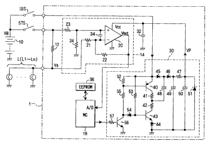
Referring to FIG. 1, a disconnection detecting apparatus
1 includes a differential amplifier circuit 14, a
microcomputer (MC) 18, a charge pump circuit 30 (charge pump
circuit), and an EEPROM 36. The apparatus 1 detects
disconnection of lamps L1-Ln. The differential amplifier
includes an operational amplifier 20. A resistor 12 for
current-voltage conversion is connected in series with a path
for supplying a current to the lamps L1-Ln.
A capacitor 32 is connected to the line that is for
supplying the voltage Vcc to the operational amplifier 20 for
stabilizing the voltage Vcc. A capacitor 34 is connected
between input terminals of the operational amplifier 20 to
reduce malfunctions caused by noise. The EEPROM 36 is a
nonvolatile memory for storing data on output errors of the
differential amplifier circuit 14. It is connected to the
microcomputer 18 in a manner that data is transferable between
the EEPROM 36 and the microcomputer 18.
-4-
CA 02410266 2006-12-18
27957-31
The charge pump circuit 30 includes a PNP transistor 40,
resistors 41, 42, 47, an NPN transistor 43, diodes 44, 45, 46,
capacitors 48, 49, 50, and a zener diode 51. The PNP
transistor 40 is supplied with voltage VB of a battery 10 via its
emitter and an ignition switch IGS. The resistor 41 is
connected to the collector of the transistor 40 and to the
resistor 42. The resistor 42 is connected to the collector of
the NPN transistor 43.
The anode and the cathode of the diode 44 are connected
to the emitter of the transistor 43 and the ground,
respectively. The anode and the cathode of the diode 45 are
connected to the emitter of the transistor 40 and the anode of
the diode 46. The cathode of the diode 46 is connected to the
resistor 47. The capacitor 48 is connected to the cathode of
the diode 45 and between the resistors 41 and 42.
The capacitors 49, 50 are connected between each end of
the resistor 47 and the ground, respectively. The zener diode
51 is connected in parallel with the capacitor 50, and its
anode is grounded.
The charge pump circuit 30 further includes resistors 52,
53, 55, 57, a diode 54, and an NPN transistor 56. The resistor
52 is connected between the emi-tter and the base of the PNP
transistor 40. The resistor 53 is connected between the
emitter of the PNP transistor 40 and the base of the NPN
transistor 43. The anode of the diode 54 is connected to the
base of the NPN transistor 43.
The resistor 55 is connected between the base of the PNP
-5--
CA 02410266 2002-10-30
transistor 40 and the cathode of the diode 54. The collector
of the NPN transistor 56 is connected to the connecting point
of the diode 54 and the resistor 55. The emitter of the NPN
transistor 56 is connected to the ground. The resistor 57 is
connected between the base of the transistor 56 and the output
port of the microcomputer 18. Most components of the charge
pump circuit 30 are constructed in chip form.
When the stop switch (brake pedal switch) STS is closed
under the condition that the switch IGS is held closed, the
battery voltage VB is applied across the resistor 12. Voltages
that appear at the ends of the resistor 12 are applied to
noninverting and inverting terminals of the operational
amplifier 20, respectively. The charge pump circuit 30
increases _the battery voltage VB to a higher voltage VP. The
voltage VP is supplied to the operational amplifier 20 for an
operating voltage Vcc. An output Vout of the operational
amplifier 20 is applied to the A/D terminal of the
microcomputer 18.
The EEPROM 36 stores output error data of the
differential amplifier circuit 14. In the manufacturing
process of the apparatus 1, a currerit Is is fed to the
resistor 12 so that the output voltage Vout becomes the
predetermined voltage S. The microcomputer 18 writes an output
error of the differential amplifier circuit 14 into the EEPROM
36. The output error is determined by calculating a difference
between an actual output voltage Vout of the differential
amplifier circuit 14 and the predetermined voltage S.
-6-
CA 02410266 2002-10-30
If a current that raises the output voltage Vout to 3 V
is fed to the resistor 12 and the actual output voltage Vout
is 3.1 V, the differential value 0.1 V is stored in the EEPRoM
36 as an output error. The microcomputer 18 corrects the
output voltage Vout by subtracting 0.1 V or the reference
voltage by adding 0.1 V for the disconnection determination.
A voltage Va that appears at the connecting point of the
resistor 12 and the lamps L1-Ln is amplified with the reversed
polarity. The output voltage Vout of the differential
amplifier circuit 14 becomes lower as shown in FIG. 6B as the
voltage Va becomes higher due to disconnection of the lamp.
When the connection is normal, the voltage Vout reaches the
maximum voltage V10. When the connection is abnormal, the
voltage Vout becomes the voltage V11.
The operational amplifier 20 has PNP transistor-type
input stages shown in FIG. 7B. An operational amplifier having
NPN transistor-type input stages is shown in FIG. 7A. This
amplifier only operates when the input voltage is in the range
between 1.4 V and the operating voltage Vcc. On the other hand,
the amplifier 20 operates when the input voltage is in the
range between 0 V and the operatiing Voltage Vcc - 1.4 V.
Because a voltage close to the battery voltage VB is
applied to the lamps L1-Ln, the input of the operational
amplifier 20 is higher than the voltage Vcc - 1.4 V. Therefore,
the operational amplifier having the NPN transistor-type input
stages is applicable. However, this amplifier cannot outputs
the voltage lower than 1.4 V. Therefore, the amplifier having
-7-
CA 02410266 2002-10-30
the PNP transistor-type input stages is used for the
operational amplifier 20.
Even so, the voltage Va, which is close to the battery
voltage VB, can be properly detected since the voltage VP,
which is higher than the battery voltage VB, is supplied to
the operational amplifier 20. Moreover, the dynamic range of
the operational amplifier circuit can be set in a wide range,
between 0 V and the maximum voltage Vmax (4.5 V in this
embodiment) that the microcomputer 18 can read. Therefore, the
amplification factor (gain) of the differential amplifier
circuit 14 can be set to a value as large as necessary.
When the voltage Vout of the differential amplifier 14 is
inputted, the microcomputer 18 compares digital data of the
voltage Vout with digital data of the reference voltage Vth.
If the voltage Vout is lower than the reference voltage Vth,
the microcomputer 18 determines that disconnection exists in
the lamps Ll-Ln, and starts a preprogrammed fail-safe
operation. The microcomputer 18 corrects the output voltage
Vout or the reference voltage Vth based on the output error
data stored in the EEPROM 36 when performing the disconnection
determination.
In the charge pump circuit 30, the transistor 56 is
turned on and off in a constant cycle by control signals from
the microcomputer 18. When the transistor 56 turns on, the
transistor 40 turns on and the transistor 43 turns off. When
the transistor 56 turns off, the transistor 40 turns off and
the transistor 43 turns on. The capacitor 48 is charged to the
-8-
CA 02410266 2002-10-30
battery voltage VB and discharged by ori/off operations of the
transistors 40, 43, 56. As a result, the capacitors 49, 50 are
charged to voltages higher than the battery voltage VB. Then,
the voltage VP increased to approximately two times higher
than the battery voltage VB is supplied to the operational
amplifier 20 as the operating voltage Vcc.
In this embodiment, the microcomputer 18 corrects the
output voltage Vout or the reference voltage Vth based on the
output error data stored in the EEPROM 36. Then, it performs
the disconnection detection. Therefore, the apparatus 1 can
perform accurate disconnection detection without being
affected by the characteristic of the differential amplifier
circuit 14. This can reduce parts calibration, especially
resistance calibration of the resistors 21-24, in the
manufacturing process of the apparatus 1.
Even though the amplification is performed only by the
differential amplifier circuit 14, the input voltage Va is
amplified large enough for the disconnection determination. As
a result, an accurate determination can be made. Even in the
case that only one of the lamps L1-Ln is disconnected, the
disconnection is properly detected. Moreover, the apparatus 1
can be constructed small in size and low in price because it
does not include noninverting amplifier circuit 16 shown in
FIG. 8. However, the apparatus 1 still provides accurate
disconnection detection.
[Second Embodiment]
Referring to FIG. 2, a disconnection detecting apparatus
-9-
CA 02410266 2002-10-30
2 includes a D/A converter 60 and a resistor 62 in addition to
the components.shown in FIG. 1.
The D/A converter 60 outputs voltages corresponding to
the digital data outputted from the microcomputer 18. Ends of
the resistor 62 are connected to the output terminal of the
D/A converter 60 and the noninverting terminal of the
operational amplifier 20, respectively. A reference voltage Vb
applied to the noninverting terminal of the operational
amplifier 20 is adjusted based on data outputted from the
microcomputer 18 to the D/A converter 60. The D/A converter 60
and the resistor 62 thus adjust a voltage to the noninverting
terminal.
The EEPROM 36 stores data that the microcomputer 18
outputs to the D/A converter 60 to reduce output errors of the
differential amplifier circuit 14. The microcomputer 18
outputs a signal to the D/A converter 60 based on the stored
data during the disconnection determination. The output
characteristics of the differential amplifier circuit 14 vary
as the reference voltage Vb varies. Therefore, output errors
of the differential amplifier circuit 14 can be reduced by
adjusting the reference voltage Vb. For this adjustment, the
data that microcomputer 18 outputs to the D/A converter 60 to
reduce the output errors is stored in the EEPROM36.
In the manufacturing process of the apparatus 2, a_
current Is is fed to the resistor 12 so that the output
voltage Vout becomes the predetermined voltage S. When the
microcomputer 18 receives an instruction signal, it adjusts
-10-
CA 02410266 2002-10-30
its output voltage to the D/A converter 60 so that the output
voltage Vout becomes the predetermined value S. The data on
the adjusted output is stored in the EEPROM 36 as an
adjustment data for the reference voltage Vb. For instance, a
current is fed through the resistor 12 for the amount that the
output voltage Vout becomes 3 V. If the measured output
voltage Vout is 3.1 V, the microcomputer 18 reduces the output
voltage of the D/A converter. Then, the output of the D/A
converter 60 at the time when the voltage Vout = 3 V is stored
in the EEPROM 36. The microcomputer 18 outputs the stored data
to the D/A converter 60 during the disconnection detection in
regular operating mode.
Therefore, the apparatus 2 can perform accurate
disconnection detection without being affected by the
characteristics of the differential amplifier circuit 14.
[Third Embodiment]
Referring to FIG. 3, a disconnection detecting apparatus
3 inc.ludes a voltage divider constructed of a pair of
resistors 64, 66 in addition to the components shown in FIG. 1.
The resistors 64, 66 are connected in series between the
terminal to which the battery voltage is applied via the stop
switch STS and the ground. A voltage that appears at the
connecting point of the resistors 64, 66 is applied to an A/D
terminal of the microcomputer 18. The battery voltage VB is
divided by the resistors 64, 66 and inputted to the
microcomputer 18. The A/D terminal for the resistors 64, 66 is
different from the A/D terminal to which the voltage Vout is
-11-
CA 02410266 2002-10-30
inputted.
The microcomputer 18 determines the battery voltage VB
based on the divided voltage. The microcomputer 18 corrects
the reference voltage Vth in response to the detected battery
voltage VB for the disconnection detection.
A data map shown in FIG. 4 is stored in a ROM included in
the microcomputer 18. The data map shows relationship between
a correction coefficient of the reference voltage Vth and the
battery voltage VB. The map may be plotted based on average
resistances of the lamps L1-Ln so that the instability in
resistances of the lamps L1-Ln does not affect.
The microcomputer 18 reads the correction coefficient
corresponding to the detected battery voltage VB from the data
map. The microcomputer 18 multiplies the reference voltage Vth
by the coefficient. The calculated reference voltage Vth is
used for the disconnection determination. The reference
voltage Vth is corrected to a higher value as the battery
voltage becomes higher. This is because the output voltage
Vout of the differential amplifier circuit 14 becomes higher
as the battery voltage VB becomes higher.
The apparatus 3 can accurately detect disconnection for
more lamps L1-Ln even when the battery voltage VB varies. That
is, a difference between the voltage Va under the normal
condition and the voltage Va under the condition that one of
the lamps is disconnected becomes smaller as the number of
lamps increases. Therefore, the voltage Vout under the
abnormal condition is higher than the voltage Vout under the
-12-
CA 02410266 2002-10-30
normal condition when the battery voltage VB increases. As a
result, the disconnection may not be properly detected. This
is the same in the case that one of the lamps L1-Ln rated in
lower watt is included and disconnected.
In the apparatus 3, the reference voltage Vth is
corrected to a higher level as the battery voltage VB
increases. Therefore, the above problems can be reduced.
[Fourth Embodiment]
Referring to FIG. 5, a disconnection detecting apparatus
4 includes a voltage divider constructed of a pair of
resistors 64, 66 in addition to the components shown in FIG. 2.
The microcomputer 18 determines that disconnection exists
when the output voltage Vout of the differential amplifier 14
is lower than the reference voltage Vth. A voltage that
appears at the connecting point of the resistors 64, 66 is
applied to an A/D terminal of the microcomputer 18. The
microcomputer 18 determines the battery voltage VB based on
the divided voltage and corrects the reference voltage Vth in
response to the detected battery voltage VB.
The reference voltage Vth is corrected to be higher as
the battery voltage VB increases. This is because the output
voltage Vout becomes higher as the battery voltage VB
increases. Since the reference voltage Vth is corrected in
response to the battery voltage VB, the disconnection
detection is performed without being affected by the variation
in the battery voltage VB.
With this configuration, the apparatus 4 can accurately
-13-
CA 02410266 2002-10-30
detect disconnection for more lamps L1-Ln even when the
battery voltage VB varies. The voltage Va under the normal
condition and the voltage Va under the condition that one of
the lamps is disconnected are illustrated in FIG. 6A. The
difference between the two becomes smaller as the number of
lamps increases. Therefore, the voltage Vout under the
abnormal condition is higher than the voltage Vout under the
normal condition when the battery voltage VB increases. As a
result, the disconnection may not be properly detected. This
is the same in the case that one of the lamps L1-Ln rated in
lower watt is included and disconnected.
However, the reference voltage Vth is corrected in
response to the battery voltage VB in the apparatus 4.
Therefore, the disconnection detection is properly performed
without being affected by the variation in the battery voltage
VB.
The present invention should not be limited to the
embodiments previously discussed and shown in the figures, but
may be implemented in various ways without departing from the
spirit of the invention.
For example, it is preferable that the differential
amplifier circuit 14 has an offset so that the output voltage
Vout is within the range that the microcomputer 18 can read.
If it is necessary to detect disconnection of m lamps out of
the lamps L1-Ln, the offset may be set so that the output
voltage Vout remains higher than 0 V even when the m lamps are
disconnected. By setting the offset, the output voltage Vout
-14-
CA 02410266 2002-10-30
corresponding to conditions of each lamp L1-Ln can be
maintained to be within the voltage range that the
microcomputer 18 can read. As a result, the apparatuses 1-4
can perform accurate disconnection detection.
In the case of detecting disconnection of m lamps out of
the lamps L1-Ln, the output voltage Vout becomes lower as the
number of the disconnected lamps increases. When m-1 lamps are
disconnected and the output voltage Vout becomes lower than 0
V, the disconnection of m lamps cannot be determined. If the
offset is set, the above situation may not occur. As a result,
further accurate disconnection detection can be performed.
Furthermore, parts calibration, especially resistance
calibration of the resistors 21-24, in the manufacturing
process of the apparatus 1-4 becomes easier. This is because
saturating conditions, in which the output voltage Vout
becomes 0 V regardless of the voltage Va, can be reduced by
setting the offset. Therefore, calibrating the resistance of
the resistors 21-24 while measuring the output voltage Vout
becomes easier since it is performed under more stable
conditions.
The D/A converter 60 may be removed from the apparatus 2
if the reference voltage Vb of the operational amplifier 20
never exceeds an operating voltage ( 5V 10% ) of the
microcomputer 18. In this case, a signal corresponding to an
adjustment data is applied from a D/A converter integrated
into the microcomputer 18 to a resistor 62.
The microcomputer 18 may calculate the correction
-15-
CA 02410266 2002-10-30
coefficient of the reference voltage Vth from a predetermined
arithmetic expression instead of the data map. In this case,
the battery voltage VB or the voltage divided by the resistors
64, 66 are used for the calculation.
The map can be a plot of the correction coefficient of
the reference voltage Vth versus the voltage divided by the
resistors 64, 66.
-16-