Note: Descriptions are shown in the official language in which they were submitted.
CA 02410268 2002-10-30
B586P04CAC~..
TUNEABLE SECONDARY AUDIO PROGRAM RECEIVER
Field of the Invention
The present invention relates to the field of useful
devices for vision impaired persons, and in particular,
audio receivers for receiving the secondary audio program
available from television programs.
Background of the Invention
A secondary audio program (S.A.P.? service is
carried within a television transmission as an
alternative to the standard audio that accompanies the
video portion of a program. The listener may choose this
secondary audio signal. A TV station can broadcast other
information to the listener, such as a second-language
audio signal or a sound track with descriptive audio
information for the sight impaired. Video descriptions
on the S.A.P. help blind and vision impaired listeners
follow the on-screen action of a television program by
providing information that is not obvious from the
original sound track. Alternatively, a stand-alone
audio program, such as a reading service like
VoicePrintT"", a round-the-clock audio service produced by
The National Broadcast Reading Service, can be delivered
to 6.3 million homes via an S.A.P. facility. For a
person with low or no vision, the cost of a TV receiver
when only audio is required is an unnecessary expense.
And its on-screen menu is impossible to access. What is
3o required is a device that can receive a signal on the
S.A.P. directly without a TV receiver.
1
CA 02410268 2002-10-30
Regulatory bodies in both Canada and the United
States now require broadcasters to provide S.A.P.-based
services such as Voiceprint or a described audio sound
track to customers in many locations. Television
broadcasters in both countries now are required to
broadcast described programming during prime-time hours.
In North America the described information is broadcast
on the S.A.P. Video description rules require TV
licensees and program distributors to include 50 hours of
described programming per calendar quarter.
What now is required by blind and sight impaired
viewers to access the described information and other
special audio services is a tuneable, inexpensive and
easy-to-use S.A.P. access device that can be operated
without a reliance on controls that sighted viewers use
to tune a specific TV channel or a S.A.P.-based service
such as a second-language audio signal distributed on the
S.A.P. feature of a television transmission.
Statement of the Invention
The present invention provides a unique and tuneable
S.A.P. access unit that enables blind and vision impaired
persons to tune to a TV channel of choice and to receive
S.A.P. program signals. Such an access device costs a
fraction of the price of a regular TV set and provides
access to all available programming that can be received
in a particular area. In one embodiment, the S.A.P.
access device comprises a cable connector, TV tuner chip,
an IF and video detector, an S.A.P. demodulator and audio
output. A micro-controller with an optional display and
a voice chip controls the operation of the receiver. In
2
CA 02410268 2002-10-30
an alternative embodiment, the S.A.P. access unit
comprises a preset macro programmable remote control, a
video cassette recorder (VCR) having an audio output and
a multi-media speaker system. The VCR is controlled by
the macro programmable remote control, and the user can
obtain the required programming by using a tactile key
pad to access the appropriate TV channel and then
clicking a single button on the control.
Brief Description of the Drawings
Figure 1 is a block diagram of a first embodiment of
the S.A.P access unit;
Figure 2 is a front view of the S.A.P. receiver of
Figure 1 with speakers on either side of the unit;
Figure 3 is a schematic diagram of the input circuit
of Figure 1;
Figure 4 is a schematic diagram of an FM receiver of
Figure l;
Figure 5 is a schematic diagram of the S.A.P
demodulator of Figure l;
Figure 6 is a schematic diagram of the multiplexer
(MUX) of Figure 1;
Figure 7 is a schematic diagram of the IF and Video
detector of Figure l;
3
CA 02410268 2002-10-30
Figure 8 is a schematic diagram of the micro
controller of Figure 1;
Figure 9 is a schematic diagram of the voice
generator of Figure l;
Figure 10 is a schematic diagram of the display
board of Figurel, and
Figure 11 is a block diagram of a second embodiment
of the S.A.P, receiver of the invention.
Detailed Description of the Preferred Embodiments
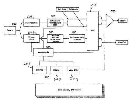
Figure 1 is a block diagram of a first embodiment of
the invention, intended to work from a TV cable or other
source of RF TV signals. A cable-in module (600)
receives the signal and feeds it to a band-pass filter
(601), and to a TV tuner (602). From the band-pass
filter, the signal is fed to FM receiver (500). If FM
signals are not required, the band-pass filter (601), and
FM receiver (500) can be omitted from the unit, with a
corresponding saving in cost. From the TV tuner (602),
the signal is fed to the IF and video detector (300).
The S.A.P. demodulator (400) is connected to the output
of the unit (300), and feeds the secondary audio program
to the multiplexes (410). The S.A.P. receiver is
operated by switches (201), which also operate the
display (202), and the voice chip (203). The voice chip
(203) sends an audio signal to the speaker (700),
3o indicating the function selected by the switches (201).
FM left and right signals, TV left and right signals,
4
CA 02410268 2002-10-30
S.A.P. audio and voice chip signals are fed to the
multiplexes (410) and are passed to amplifiers and stereo
equipment as required, as shown in Figure 7, and
described below.
Figure 2 illustrates the front panel and speakers of
the embodiment of Figure 1. Not shown are connectors for
cable and aerial antenna, which would in the usual way be
located on the rear of the unit. The controls (201) are:
a power switch (30) preferably a push button spring type,
a signal mode selector (31) preferably an up/down centre
off switch, a channel selector up/down switch (32), and a
status announcement button (33). A status panel
including LED readout shows the channel in a 4 digit
numeric display, and a combination LED displays Cable
TV/FM/S.A.P. Speakers (701) and (702) are shown on
either side of the unit.
Figure 3 in schematic form shows the input circuit
(600) of the unit (200) including the band-pass filter
(601), and the outputs for the FM receiver (500) and for
the TV tuner (602). The components and values are chosen
to provide the required separation and band-pass required
for the FM and TV inputs, which are within the ordinary
skill of a circuit designer.
Figure 4 is a schematic diagram of the FM receiver
(500) of Figure 1. The circuit is provided with 5 volt
DC power and two ICs are used, a TDA7021T and TDA7040T.
The output from the band-pass filter (601) of Figure 3 is
received at FM-in (501) at pin 12 of TDA7021T, and is
5
CA 02410268 2002-10-30
converted to FM left and FM right audio signals (502) and
(503), respectively.
Figure 5 is the S.A.P. decoder, or demodulator
(400), which receives the base band Audio at (401) from
the from the IF and video Detector (300) of Figure 1 and
outputs the S.A.P. audio at (402) and the TV left and
right sound at (403) and (404), respectively. The signal
processing is performed by the IC TDA3833.
Figure 6 is a schematic of the multiplexer (410) of
Figure l, which is controlled by the micro controller
(100) of Figure 1. Audio inputs FM left, FM right, TV
left, TV right, S.A.P. and voice from the voice chip
(203) are passed to the outputs Left Out, Right Out and
to Audio Amp, under control of signals FM ctl,TVctl,
S.A.P.ctl, and voice from the micro controller (100).
Suitable amplifiers (411) and (412) amplify the outputs
of the MUX (410) as required.
Figure 7 is a schematic of the IF and video detector
(300) of Figure 2. Ics MC1350P and MC1330P receive and
amplify the IF input at (301), and output the base band
audio at (302) which is input to the S.A.P, demodulator
(400). Component values as illustrated are chosen for
the desired operation of the circuit and are within the
scope of the circuit designer.
Figure 8 is a schematic diagram of the micro
controller (100). An IC (101) shown as 87C51 provides
control signals to all components of the unit as
6
CA 02410268 2002-10-30
required. TV control signal (TVctl) is output at pin 19
of the IC and through circuit (102) toggles between TV
and FM signals being fed to the MUX (410). Similarly,
the S.A.P. signal at pin 20 of IC (101) controls the
output of S.A.P. demodulator and passes S.A.P. audio at
pin 402 of unit (400) (Figure 5). Once again the
selection of specific components is within the skill of a
circuit designer.
Figure 9 is a schematic circuit of the voice chip
(203) of Figure 1. An IC TSP53C33 generates voice
signals under command of the micro controller (100),
which are fed to the MUX (410) and to the output (700).
Figure 10 illustrates a schematic for the display
board (34) of Figure 2. A series of LED symbols are
shown together with the drivers and control circuits.
Table 1 below illustrates component values and
specifications for the components of Figures l to 11.
7
CA 02410268 2002-10-30
SAP board 10117I2fl01
main Part 16:54
list
(
ND
FM
receiver
- QTY Descri P!N Di iKey PlN
tion
Value
2 Resistor, 1t4 Watts 5~ GarbonQBK BD
5~ Film
1l4
W'
3 Resistor, 114 Watts 5% CarbonQBK:BD
5r6114 Fiim
W
27
i Resistor, 114 Watts 5h CarbonQBK-BD
5% Film
174
W
130
1 Resistor; 1l4 Watts 5l CarbonQBK BD
5% Film
1l4
W
160
1 Resistor, 114 Watts 5% CarbonQBK-BD
5% Fitm
114
W
980
2 molded Deievan,1641-121' DN41121-ND
RF
wits
0.12uH
3 Ceramic Panasonic ECU-S1J104KBBP4887-ND
Ca
acitor,
radial
0.luF
63V
1 Ceramic Panasonic ECU-S1J474MEBP4919-ND
Ca
acitor,
radian
0.47
uF
63V
1 Elect: PanasonicfCE-BIJGEi02t'5490-ND
Capacitor,radiai
1000uF
63V
1 Vofumn CT2219-ND
Control
Pot,
with
ONIOFF
100K
1 Power Delevan, 2474-2bL ON7425-ND
inductor
100uH
_ 8 Ceramic Panasonic ECU-$1J103KBAP4904-ND
Ca
acitor,
radian
lOn
63V
- 13 Erect.citor,radiat IOuF 16V Panasonic ECE-A16Z10P6616-ND
Ca
1 TerminalPost 11 contacts INN4009-ND
1 Resistor, 1/4 Watts 5~ CarbonQBK-BD
5% Film
114
W
.
110K
1 Wall Cui DPD120080-P-5 T507-ND
Transformer
12V
800mA
2 Resistor; 114 Watts 5% CarbonQBK-BD
5~ Fitm
1I4
W
1i(
2 Resistor,:5.G 114 Watts 5%-CarbonQBK BD
114 Film
W
.
1K8
1 Resistor, 1I4 Watts 5~ CarbonQBK-BD
5~ Film
1l4
W
1K8
1 Silicon 1N4002CT-ND
Diode
1N4002
1 Shottk 1 N5819CT-ND
Diode
1
N5819CT
6 Ceramic Panasonic ECU-S1J102JCBP4812-ND
Ca
acitor,
radial
1nt=
63V
16 Tantalum. Panasonic ECS-F1CE105KP2105-ND
Ca
acitor,radial
1uF
16V
8 Terminal WN4000-ND
Post
2
contacts
3 Resistor, 1l4 Watts 5.5 CarbonQBK-BD
5% Fiim
1l4
W
20K
'
2 Ceramic Panasonic ECU-S1 P4889-ND
Ca J224KBB
acitor,
radial
220n
63V
3 Resistor, '114 Watts 5~ CarbonQBK-BD
561/4 Fiim
W
22K
7 Trimmer, 3299W-253-ND
Multitum
'
25K
1 Resistor, 1l4 Watts 5~ CarbonQBK-BD
S% Fiim
1141N
21c2
1 Resistor, 9I4 Watts 5~ CarbonQBK-BD
5% Fitm
1/4
W
2K?
2 Terminal tNN4001-ND
Post
3
contacts
2 Ceramic Panasonic ECU-S2A3390JCAP4844-ND
Ca
acitor,
radial
39
F
100V
12 Resistor, 114. Watts 5% CarbonQBK-BD
~ 5% Film
114
W
4.7K
4 Resistcx, 1l4 Watts 5~ CacbonQBK BD
5% Film
1/4
W
4:7K
2 Erect. Panasonic ECS-A1VGE471P5260-ND
Ca
acitor,radiat
470uF
25V
1 Ceramic Panasonic ECU-S1 P4885-ND
Ca J473KBB
acitor,
radial
47nF'
631/
2 Elect: Panasonic ECS-A1VGE4R7P5252-ND
Ca
acitor,radial
4u7F
351/
8
CA 02410268 2002-10-30
1 Terminal Post __,_"-5 contacts WN4003-ND
-
1 Trimmer, Multiturn 50K _ 3299W-503-ND
_
1 Resistor; 5x,114 56K _ QBK-SD
W 114 Watts 5% Carbon
Film
1 RFcoils ! 56nH Panasonic ELJ-ND5fiNJFCD1169CT-ND
2 Ceramic Ca acitor, 56 F 100VPanasonic ECU-S2A560JCAP4846-ND
radial
1 Resistor, 5% 1l4 75K 114 Watts 5% Carbon QBK-BD
W Film
1 Voltage Regulator 78M12
~
1 Resistor, 5% 1I4 8K2 1I4 Watts 5~ Carbon QBK-BD
W Film
1 Philli sRF Tuner FR1236
1 Switch Mode Volta LM2575T-50
a Controller
1 S Baker amp MC34199
3 Resistor, 5% 1I4 T8D 114 Watts 5~ Carbon QBK-BD
W Fifm
1 TV Sound Process TDA3833
r
1 Op Am TL082 JFET OP-Amp, DIP
3 Ceramic Ca acitor, xxpF Optional
radial
LED High ifcienc RED HLMP-1700QT-ND
LED
1 Coaxial Power Jack, PJ-002A CP002A-ND
2.OMM
1 Slide Siwtch,SPOT C&K 1101M2S3ABE2 CKN5005-ND
2 Analog Siwtch CD4D66BE CD4066BE-ND
1 Plastic Enclosure 6.32" X 8.10" X 2.52"
1 Stero Jack, 118 in CP-3505-ND
dia. anet Mount
1 Interconnect Cable
1 Speaker, 2.2"
1 Knobes
2 Ty a F connector,
RCA cable .
4 Switch. momentary,spst CKN4051-ND
1 Nuts, #4
1 Screws #4
1 Switch. momenta ,s CKN4051-ND
st
1 Switch. momenta ,spst CKN4051-ND
1 Switch. momenta ,spst CKN4051-ND
9 T pe F connector,
RCA cable
1 PCB, Main board '~ -
9
CA 02410268 2002-10-30
SAP la board Part _. 1011712001
dis fis! 17:01
~
QTY Description Yatue PM DigiKe '
PlN
C101Ceramic Ca dtor39 Panasonic ECU-S2A3390JCAP484~4-ND
' radial 100V
C102Ceramic Ca c~or39IaQV Panasonic ECU-SZA3390JCAP4844-ND
radial
C103Ceramic Ca citor;1nF Panasonic ECU-S1J102JCBP4812-ND
radial 63V
C104Ceramic Ca acitor;1 Panasonic ECU-S1Jf02JCBP4812-ND
radial nF
63V
C108Ceramic Ca cnor39 Panasonic ECU-SZA3390JCAP4844-ND
radial 100V
C109CeramicCa cifor39 Panasonic ECU-S2A3390JCAP4844-ND
. radial F.108V
C110Tantalum: Ca luF Panasonic ECS-F1CE105KP2105-ND
acitor,radial 16V
C111Tantalum. Ca 1uF PanasonicECS-F1CE105KP2105-ND
atorradial 16V
C112Tardatum: Ca 1uF Panasonic ECS-F1CE105KP2105-ND
c~ar;radial 16V
C113Ceramic Ca actor;22nF' Panasonic ECU-S1J223KBAP4884-ND
radial
C114Eiec~t. Ca citor,radiatlOuF Panasonic ECE P8616-ND
- 16V A16Z10
C115Ceramic Ca citor,10n Panasonic ECU-S1J103KBAP4904-ND
radial E33V
C118Elect. Ca citor,radial10uF PanasonicECE-A16Z1aP6616-ND
18V
C118Ceramic Ca citor,1nF Panasonic ECU-S1J102JCBP4812-ND
; radial 63V
D100LED, Red H' h Effiaen RED HLMP-1700QT-ND
LED
Di01LED, Red H' h Eflicten HLMP-1700QT-ND
REO LED
D102LED, Red Hi h Efficien HLMP-1700QT-ND
RED LED
D103LED, Red H' h Effiaenc HLMP-1700C1T-ND
RED LED
D104t-ED Red H' E~Cien RED HLMP-1700QT-ND
LED
P1 Terminal Post 11 ED7211-ND
contacts
P2 Terminal Post 3 ED7203-ND
contacts
P3 Terminal Post 6 ED7206-ND
contacts
Q100NPN Transistor 2N3904 2N3904-ND
Q101NPNTransistor 2N3904 2N3904-ND
Q102NPN TraOr 2N3904 2N3904-ND
Q103NPN Transistor 2N3904 2N3904-ND
'
Q104NPN Transistor 2N3904 2N3904-ND
Q105NPN Transistor 2N3904 2N3904-ND
Q106NPN Transistor 2N3904 2N3904-ND
Q107NPN Transistor 2N3904 2N3904-ND
8100Resistor; 5% 4K7 114 Watts 5% CarbonQBK-BD
~/4 W Film
8101Resistor, 5% 100K 114 Watts 5% CarbonQBK-BD
114 W Film
8102Resistor, 5% 20K 114 Watts 5~ CarbonQBK-BD
1l4 W Film
8103Resistor, 5% 10K 1/41N9tts 5% CarbonQBK-BD
114 W Film
8104Resistor 5% 20K 114 Watts 5% CarbonCtBK-BD
114 V1t Film
8105Res~tor; 5% 20K 1J4 Waths 5% CarbonQBK BD
1/4 W Flm
8106Resistor, 5% 20K 114 Watts 5~ CarbonQBK-BD
114 W Fiim
8107Resistor, 5% 20J< 1/4 Watts 5% CarbonQBK-8D
1/4 W Fdm
8108Resistor 5% 20K 114 Watts 5% CarbonQ$K-BD
1l4 W Film
8109Resistor, 5% 20K 1/d Watts 5% CarbonQBIC BD
114 W Film
8110Resistor, 5~ 20K 114 Watts 5~ CarbonQBK-BD
114 W Film
8111Resistor; 5% 20K 1l4 Watts 5% CarbonQBK-BD
1l4 W Film
Rli2Resistor, 5% 47 l/4Watts 5%CarbonQBK BD
t/4 W Film
8113Resistor; 5% 47 114 Watts 5% CarbonQBK-BD
1l4 W Film
R1 Resistor, 5% 47 1l4 Watts 5% CarbonQBK-BD
f4 1l4 W Fdm
8115Resrsfor; 5% 47 1/4 Watts 5% CarbonQBK-BD
914 W Film
8116Resistor, 5% 47 114 Watts 596 QBK-BD
1l4 W Carbon Fiim
8117Resistor, 5~ 4T 114 Watts 5% CarbonQBK-BD
1l4 W Fiim
8118Resistor,,5% 47 t14 Watts S% CarbonQBK-BD
114 W Film
8119Resistor; 5~ 47 1/4 Watts 5% CarbonQBK-BD
114 W Ffim
8120bare wire 0
8121bare wire 0
8122bare wire 0
_ bare wire
Rf
23
CA 02410268 2002-10-30
8124 Resistor, 5% 1!4 Watts 5~ QBK-BD
i!4 W 510 Carbon Film
R'125 Resistor, 5% 1!4 Wads 5% Carbon_
1!4 W 510- Fiim QBK-BD
8126 Resistor; 5% 1!4 Watts 5~ QBK-BD
~ 1i4 W 510 Carbon Film
8127 Resistor; 5% 114 Watts S% QBK-BD
~ 114 W 5i0 Carbon Fitm
8128 Res~tor, 5% 1!4 Watts 5~ QBK-9D
1/4 W 1K Carbon Film
0100 Microcontraller 87C751
0101 F~PROM MG24C16
0102 Voice Chip TSP53C33
'
0103 O AMP 'fl-082 JFET OP-Amp,
D1P
U104 Micro Monitor DS1232
U105. Serial Latch 74FCi84
U106~ LED decoder MC14499
U10T 7 meets Di FND357
a
U108 7 s meets Dts FND357
a
0109 7 meets D' FND357
a
0110 7 s meets Dts FND357
la
U112 microcontroller, AT89C205i
o tionat
Y700 C 1 11.0592MHz
YlOi G stal 7.6
16 'ns tC Socket
ED31 i6-ND
8 ins IC Socket
ED31-8-ND
24 ns IC Socket
0.300 in wide
, ED3124-ND
PCB, dis la
board
US$
11
CA 02410268 2002-10-30 '"'
Figure 11 is a block diagram of a second
embodiment of the invention. In this embodiment, a VCR
(20), which is controlled by a macro programmable remote
control (21), such as that sold under the brand "One For
All Cinema 6" provides a one button accessible S.A.P.
access unit . The control (21) is programmed so that a
single button is all that needs to be operated for
obtaining an audio output (22), which can be fed to a
multimedia speaker system (23). The VCR (20), is
connected to cable or antenna inputs (24) and (25), and
the desired TV channel is selected by pressing the
appropriate tactile keys on the remote (21). The S.A.P.
signal is then selected and output through the audio
output (22) to the speaker system (23). A suitable VCR
is a Sharp model VC-H960 HI-FI Stereo Video Cassette
Recorder. The VCR used must be stereo and would
therefore have S.A.P. capabilities.
12