Note: Descriptions are shown in the official language in which they were submitted.
CA 02410496 2002-11-28
WO 01/94979 PCT/SE01/01252
1
RADIATION DETECTION APPARATUS AND METHOD
TECHNICAL FIELD OF THE INVENTION
The present invention generally relates to an apparatus and
method for detection of ionizing radiation, particularly but not
exclusively X-rays.
The invention is usable in a variety of fields including e.g.
medical radiology, computerized tomography (CT), microscopy, and
non-destructive testing.
DESCRIPTION OF RE?~ATED ART AND BACKGROUND OF THE INVENTION
Scintillator based detection systems are widely used for high-
resolution imaging of gamma and x-rays. Such imaging systems use
the detected radiation to produce a signal, which can be used to
operate a visual display, such as a cathode ray tube.
One example of such an imaging system is the Anger camera, which
is commonly used in medical diagnostic procedures. In the Anger
camera, incident radiation passes through a collimator before
striking a scintillator layer. Light generated by the
interaction of the incident radiation and the scintillator
material then spreads out through an underlying light guide
until it strikes an array of photomultipliers. The intensity of
the light striking the individual photomultipliers varies
dependent on the distance of the photomultiplier from the point
where the incident radiation interacted with the scintillator to
produce the initial light burst. A resistor network electrically
determines the point of the radiation impact on the array based
upon the magnitude of the respective electrical output of the
photomultiplier devices in the array; summing the electrical
output signals provides a measure of the energy level of the
initial incident radiation. The low efficiency of the light
guide and the poor photoemission conversion of the
CA 02410496 2002-11-28
WO 01/94979 PCT/SE01/01252
2
photomultipliers result in significant statistical fluctuation
of collected light photons, which causes degraded spatial and
energy level resolution. Additionally, Anger cameras have
relatively low count rates as every incident gamma ray that
interacts with the scintillator material results in
substantially the entire array being rendered non responsive
until the light generated from the earlier interaction has
diminished.
Another common prior art device is known as an image intensifier
gamma camera. In such devices, the scintillator is shaped to be
tightly coupled to the transparent window of a large field of
view image intensifier tube, which discharges photoelectron
energy packets' in response to the light signal from the
scintillator. The photoelectron packets are accelerated and
focused onto a cathodoluminescent phosphor deposited on a fiber
optic output plate, generating additional light photon bursts.
Multiple image intensifier stages can be coupled together to
further amplify the signal. The final burst of photoelectrons
will generate charges on a resistive charge divider from which
the center of gravity of the pulse is reconstructed. Image
intensifier cameras have substantial weight, size and expense,
which inhibit their practical use for many applications.
A solid-state radiation detector is disclosed in U.S. Pat. No.
5,144,141. In this detector, radiation incident on the detector
passes through a collimator and strikes a scintillator, which is
divided into a plurality of scintillator elements arranged in
rows and columns. An array of internal gain photodetectors
divided into rows and columns are optically connected to the
scintillator elements. Each photodetector is electrically
coupled to a respective detect and hold circuit which amplifies
and stores the pulse generated by the photodetector; the stored
pulses are sampled via a multiplexed switching arrangement to
allow the stored signal from each detect and hold circuit to be
processed to produce a digitized imaging signal which
CA 02410496 2002-11-28
WO 01/94979 PCT/SE01/01252
3
corresponds to the energy level of, and location on the array
of, the detected incident radiation. The digitized imaging
signal is supplied to display memory and analysis equipment for
the device.
Particularly for radiation imagers employed in medical
procedures, in which it is desired to expose the patient to the
minimum amount of ionizing radiation as possible, it is
important that the imaging device be sensitive to low levels of
radiation while still being able to discriminate against
background radiation. Solid-state detectors have a somewhat
limited amplification due to losses, and thus in some
application they do not possess sufficiently high signal-to-
noise ratios.
Improved spatial resolution requires the use of a large number
of photodetectors and a scintillator system, which generates
light photons only in the scintillator segment in which the
incident radiation was absorbed. The use of a larger number of
photodetectors in a large array or to increase the resolution of
the device rapidly results in very complex and expensive
apparatus.
Further, photodetectors are sensitive to direct irradiation by
the incident X-rays and hence measures have to be taken in order
to prevent the incident radiation from reaching the
photodetectors.
Additionally, solid-state radiation detectors have a limited
speed. They normally require long integration times in the
electronics, several microseconds, in order to capture a large
fraction of the signal and keep down the noise level. This
prevents them in most applications to be used for single photon
detection. Additionally the noise level in solid state detectors
is normally too high to be able to detect single photons.
CA 02410496 2002-11-28
WO 01/94979 PCT/SE01/01252
4
SUMMARY OF THE INVENTION
Accordingly, it is an object of the present invention to provide
an apparatus and method for detection of ionizing radiation,
particularly X-rays, which provide for an effective
amplification and high signal-to-noise ratios.
A further obj ect of the invention is to provide such detection
apparatus and method, which provide for high sensitivity, and
can thus operate at very low X-ray fluxes.
Yet a further object of the present invention is to provide such
detection apparatus and method, having detection elements, which
are insensitive to direct irradiation by the ionizing radiation.
Still a further object of the present invention is to provide a
detection apparatus and method, which are capable of detecting
and resolving single light photons emitted from a scintillator
by a single X-ray. This allows a more accurate determination of
the X-ray energy than conventional integrating techniques.
Yet a further object of the present invention is to provide such
detection apparatus and method, which are effective, fast,
accurate, reliable, and of low cost.
These objects among others are, according to the present
invention, attained by apparatus and methods as claimed in the
appended Claims.
By employing avalanche amplification of electrons released from
the photocathode of the detection apparatus in a gas a
particularly sensitive apparatus and method are achieved, which
provide for the employment of extremely low doses of radiation,
still obtaining signal levels high enough for construction of
two-dimensional images exhibiting very low noise levels.
Further, extremely good spatial resolution can be achieved
without the need of evaluating a central point of detection.
CA 02410496 2002-11-28
WO 01/94979 PCT/SE01/01252
This means that the detector is fast and can thus operate at
very high radiation fluxes.
A further advantage of the inventive detector is that it is not
very sensitive to magnetic fields.
5 Yet a further advantage of the invention is that it provides for
the manufacture and use of sensitive large-area detectors to a
low cost.
Further characteristics of the invention and advantages thereof
will be evident from the following detailed description of
preferred embodiments of the invention, which are shown in the
accompanying drawings.
BRIEF DESCRIPTION OF THE DRAWINGS
The present invention will become more fully understood from the
detailed description of embodiments of the present invention
given hereinbelow and the accompanying Figs. 1-2, which are
given by way of illustration only, and thus are not limitative
of the invention.
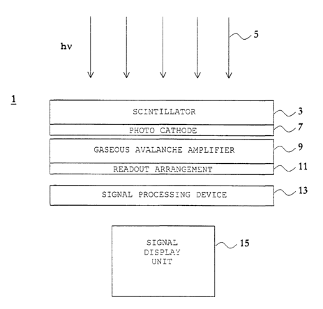
Fig. 1 illustrates schematically the main components of a
detector apparatus according to the present invention.
Fig. 2 illustrates schematically, in a cross sectional view, a
particular embodiment of the detector apparatus according to the
invention.
DETAIT~ED DESCRIPTION OF PREFERRED EMBODTMENTS
In the following description, for purposes of explanat~_on and
not limitation, specific details are set forth, such as
particular dimensions and materials in order to provide a
thorough understanding of the present invention. However, it
will be apparent to one skilled in the art that the present
invention may be practiced in other embodiments that depart from
CA 02410496 2002-11-28
WO 01/94979 PCT/SE01/01252
6
these specific details. In other instances, detailed
descriptions of well-known apparatus and processes are omitted
so as not to obscure the description of the present invention
with unnecessary details.
With reference to Fig. 1, which schematically illustrates the
main components of an inventive detector apparatus Z, the
general principles of the present invention will be depicted.
The detector apparatus comprises a scintillator device 3, the
front surface of which being directed towards the ionizing
radiation 5 to be measured. The radiation is converted into
light within scintillator device 3 through various physical
interactions, which will be described closer below. The
scintillator is a solid converter or it may comprise a liquid
scintillating substance, e.g. liquid xenon or argon, or a solid
scintillating substance.
The radiation is preferably X-rays, but the invention is useful
with any kind of ionizing radiation that a scintillator device
is capable of converting into light.
Further, a photocathode 7 is arranged at the back surface of
scintillator 3, which is arranged such that it releases
photoelectrons in dependence on the light photons that hit it.
The cathode shall be thin such that it is capable of releasing
electrons from the surface opposite to the surface onto which
the photons axe impinging.
An electron avalanche amplification apparatus 9 is arranged
next to photocathode 7. Avalanche amplification apparatus 9 is
preferably provided with two electrodes; an avalanche cathode
and an avalanche anode (not indicated in Fig. 1), and. is
adapted to collect photoelectrons released from photocathode 7
and to strongly avalanche amplify these. Geometries and
amplification material of electron avalanche amplification
apparatus 9 and electric potentials, at which the avalanche
CA 02410496 2002-11-28
WO 01/94979 PCT/SE01/01252
7
electrodes are held, are selected such that a suitable
amplification is obtained.
Electron avalanche amplification apparatus 9 comprises a closed
chamber between the electrodes containing a gas suitable for
electron avalanche amplification. Such suitable amplification
gas include for instance xenon, or mixtures of xenon and argon.
Further, detector apparatus 1 comprises a read-out arrangement
11, preferably located in the vicinity of the avalanche anode,
the arrangement being adapted to detect pulses induced by the
avalanche electrons and/or correspondingly produced ions. Read-
out arrangement 11 is connected a signal processing device 13
for necessary and/or desired post-processing of collected
signal data. A signal display unit 15 is finally provided for
displaying the processed signal data.
By using the principles of the present invention, i.e. by
converting the light from the scintillator into electrons and by
avalanche amplifying these in a suitable gas before detection,
instead of using a conventional scintillator detector, a fast
and sensitive detector is obtained to a low cost. The
amplification is more effective than with conventional solid-
state based detectors.
Next, with reference to Fig. 2, which schematically, and in a
sectional view, illustrates an inventive detector apparatus 21,
a particular embodiment of the present invention will be
discussed in more detail.
The apparatus 21 includes a plurality of scintillator elements
23 arranged in an array 25 and exposed to incident radiation 27,
Eaoh scintillator element is optically coupled to a photocathode
arrangement 29 including a photocathode layer 31 and an optional
protective layer 33. A gaseous electron avalanche amplification
detector 35 is arranged adjacent to photocathode arrangement 29,
the detector including an array 36 of readout elements 37, each
CA 02410496 2002-11-28
WO 01/94979 PCT/SE01/01252
8
of which is electrically coupled to a signal processing circuit
39 by means of a respective signal conduit 40. The signal
processing circuit 39 may further be connected to a signal
display indicator (not shown in Fig. 2).
Incident radiation 27 typically comprises x-rays. The structure
of the detector apparatus of the invention is, however,
adaptable to the detection of other types of radiation provided
that appropriate scintillator material and radiation absorbent
material in any interstitial barriers are selected. For ease of
description, incident radiation is referred to herein as rays,
although, dependent upon the type of radiation to be detected,
particles or other nomenclature. known in the art may similarly
be.used to describe the radiation. Radiation is used to refer to
the electromagnetic energy the imaging device is to detect (e. g.
x-rays), and the words Light or optical are used to refer to the
light energy or photons that are produced by the scintillator
material when it interacts with the incident radiation. In
typical imaging devices, the energy level of the incident
radiation ranges between about 10 keV and 500 keV. In this
energy range, typical interactions between the incident
radiation and the scintillator material include photoelectric
absorption and Compton scattering. Both of these processes
result in electrons being emitted from atoms in the scintillator
that are struck by the incident ray,. and as these electrons pass
through the scintillator material their energy is converted to
visible radiant light energy.
A collimator 41 is optionally disposed adjacent to scintillator
array 25 so that the collimator overlies the scintillatoz array.
Collimator 41 is positioned on detector apparatus 21 so that
radiation incident on the device must pass through collimator
passages 43 to enter scintillator elements 23. For ease of
illustration, only a limited number of passages 43 are shown in
FIG..1; it should be noted, however, that collimator 41 would
typically have a large number of such passages, which would be
CA 02410496 2002-11-28
WO 01/94979 PCT/SE01/01252
9
in coincidence with the underlying scintillator elements. The
collimator preferably is comprised of lead, or any other high
atomic number element.
The scintillator elements 23 forming array 25 typically form an
MxN matrix, but can alternatively be in any shape appropriate
for the employment of a particular apparatus. The scintillator
elements typically have a parallelepiped shape, and may, by way
of example and not limitation, have cross-sectional dimensions
of 0,.01 - 0.1 mm x 0.01-0.1 mm (to provide for detection with
high spatial resolution) and a depth of 0.1-100 mm. The
scintillator array can be formed by cutting, or dicing, the
elements from one block of scintillator material or
alternatively the elements can be individually ~ "grown" as
needles or rods e.g. by evaporation or other known techniques
such as sputtering or chemical vapor deposition. In a large area
array, such as would be used for medical imaging purposes, an
array may typically have many thousands of scintillator elements
and have outer dimensions of up to 50 cm x 50 cm. A small area
array used for some applications may be smaller than 1 mm x 1
mm. Scintillator elements 23 preferably are formed of a material
having a relatively high efficiency for converting the incident
radiation to optical energy, a relatively fast decay constant,
and good optical transparency. Cesium iodide has proven to be a
good scintillator material for the detection of x-rays, having a
high conversion efficiency, a decay constant of 1 microsecond,
and a refractive index of 1,8. Alternatively, other known
scintillator materials, such as for instance NaI, BaF~ or
polymeric materials, may be used in the device of the present
invention.
In accordance with the present invention, interstitial barriers
45 may optionally be disposed between the scintillator elements
23 so as to separate each scintillator element from adjoining
elements. Interstitial barriers 45 comprise a material that
effectively absorbs incident and secondary radiation rays,
CA 02410496 2002-11-28
WO 01/94979 PCT/SE01/01252
thereby substantially preventing light from passing between
scintillator elements. Such a light absorptive barrier is
particularly important in large area devices to ensure good
spatial.resolution, i.e. determination of the location on the
5 array where the incident radiation ray strikes.
Optically reflective layers 47 may optionally be disposed
between the adjoining surfaces of interstitial barriers 45 and
the scintillator elements 23, and possibly across the portion of
scintillator array 25 through which the incident radiation
10 enters (not shown in Fig. 2). Optically reflective layers 47
serve to isolate the scintillator elements from one another by
confining within one scintillator element the visible light
generated by the absorption of incident radiation in the
element. Reflective layers 47 comprise relatively thin, i.e.,
about 0.01 ~.un to 0.5 ~,m layers of silver, aluminum, or similar
material that is optically reflective and radiation
transmissive, i.e. does not substantially interact with the
incident radiation. Reflective layers can be, but need not
necessarily be, deposited on all scintillator element surfaces.
The photocathode arrangement 29 includes the photocathode layer
3l, which preferably is a 0.00001-0.1 mm thick layer of e.g. CsI
or, an organic photo converter or any other efficient gaseous,
liquid or solid photo converter, and the protective layer 33,
which preferably is a 0.01-1 ~m thick layer of a e.g. CsI.
Photocathodes are generally sensitive to small impurities in any
gas in contact with it, which impurities cause degradation of
the quantum efficiency of the photocathode with time. Thus, the
protective layer 33 shall protect the cathode layer 31 from
direct contact with the amplification medium, i.e. the avalanche
gas, of the avalanche amplification detector 35, but shall be
transparent to the electrons released from the photocathode
layer surface. Further, the protective layer shall
advantageously be opaque to light since there may occur
CA 02410496 2002-11-28
WO 01/94979 PCT/SE01/01252
11
fluorescence in electron avalanche amplification detector 35 and
this fluorescence light has to be prevented from reaching the
photocathode layer and thus from striking out more electrons,
which would affect the detection in an unwanted manner. If the
protective layer is not opaque to light it may be covered by a
thin metallic layer, which is opaque to light and transparent to
electrons.
The electron avalanche amplification detector 35 comprises
sidewalk 49, which together with photocathode arrangement 29
and the array 36 of readout elements constitute an airtight
housing. The interior of this housing constitutes an optional
drift and amplification volume 51 and is filled with a gas
suitable for electron avalanche amplification, which can be for
example C02 or a mixture of for example helium and isobutane, or
any other gas suitable for electron avalanche multiplication.
The gas is preferably at atmospheric pressure, but can be both
at under- as well as overpressure. A pressure close to
atmospheric is preferred if an appropriate avalanche
amplification can be achieved at such pressure is since any
requirements on windows etc. to resist a high pressure (or
vacuum) are relaxed.
Alternatively, the detector itself is not encasing the avalanche
amplification substance, but is placed within an external
containment.
Still alternatively, a circulating system is provided such that
the gas can be flushed through the detector chamber, optionally
filtered, and then re-circulated to the detector chamber.
Further, electron avalanche amplification detector 35 comprises
an avalanche cathode arrangement 53 and an avalanche anode
arrangement, which, in the present embodiment, is identical with
the array 36 of readout elements 37. Avalanche cathode 53 is
preferably of an electrically conducting material and avalanche
CA 02410496 2002-11-28
WO 01/94979 PCT/SE01/01252
12
anode arrangement 36 includes typically an insulating substrate
54 wherein the readout elements 37, being of an electrically
conducting material, are arranged.
Alternatively, the avalanche anode can be formed separated from
the read-out arrangement 36 (not shown in Fig. 2).
The electric potentials, at which the photocathode 29, the
avalanche cathode 53, and the avalanche anode 36 arrangements
are held, are selected such that a weaker electric field, a
drift field, is created between photocathode 29 and avalanche
cathode 53 causing drift of photoelectron s released from the
photocathode arrangement 29 towards avalanche cathode 53, and a
stronger electric field, an avalanche amplification field, is
created between avalanche cathode 53 and avalanche anode 36,
causing avalanche multiplication of the photoelectrons as they
are accelerated towards avalanche anode, or array of readout
elements, 36. Electrical field lines between a single one of the
readout elements 37 and the photocathode arrangement 29 are
schematically indicated in Fig. 2 by reference numeral 55 for
illustrative purposes.
A dielectric 57 may be arranged between avalanche cathode 53 and
avalanche anode 36. This could be a gas or a solid substrate
carrying cathode 53 and anode 36, as shown in Fig. 2. Thus, the
applied voltages produce a strong electric field in an array of
avalanche amplification regions 59. The avalanche regions 59 are
formed in a region between and around the edges of the avalanche
cathode 53 which are facing each other, and between the
avalanche cathode 53 and the avalanche anode 36.
The avalanche regions 59 are formed by openings or channels in
cathode 53 and in the dielectric substrate 57, if present.~The
openings or channels can be of arbitrary shape, e.g. having a
circular or a square cross section. The openings or channels may
be arranged in rows, each row of openings or channels including
CA 02410496 2002-11-28
WO 01/94979 PCT/SE01/01252
13
a plurality of openings or channels. A plurality of longitudinal
openings or channels or rows of channels are formed beside each
other, parallel with each other or with the incident X-rays.
Alternatively, the openings or channels can be arranged in other
patterns.
Preferably, the collimator passages 43 of the collimator 41, the
scintillator elements 23 of the scintillator 25 and the
avalanche regions 59 of the avalanche detector 35 are aligned
and overlie each other.
Further, the readout elements 37 are arranged in connection with
the openings or channels forming the avalanche regions 59.
Preferably at least one element 37 is provided for each opening
or~channel. The elements 37 are electrically insulated from each
other by means of the dielectric substrate 54, and separately
connected to the signal processing circuit 39 by means of the
individual signal conduits 40.
By providing a two-dimensional array of collimator passages 43,
scintillator elements 23, avalanche regions 59 and read-out
elements 37 a detector apparatus 21 may be obtained, wherein
electron avalanches derivable mainly from ionization by
transversely separated portions of the incident radiation beam
27 are separately detectable. Hereby, apparatus 21 provides for
two-dimensional imaging. Similarly, by employing one-dimensional
arrays of respective elements an apparatus for one-dimensional
imaging is obtained.
It is preferred that the readout elements 37, the avalanche
regions 59, the scintillator elements 23, and optiona~.ly any
collimator passages 43 have the same pitch and that they are
aligned with each other. By such provisions a very good spatial
resolution can be obtained (actually limited by the pitch of the
readout elements 37, the avalanche regions 59, and the
scintillator elements 23). In a preferred version embodiment the
CA 02410496 2002-11-28
WO 01/94979 PCT/SE01/01252
14
pitch, i.e. the distance between the centers of two adjacent
regions or elements, is small enough to provide for a position
resolution in the sub-millimeter region. Preferably, the pitch
is less than 1 mm, and more preferably between 0.01 and 0.5 mm,
or between 0.01 and 0. 1 mm.
In operation, the detector apparatus 21 of Fig. 1 is positioned
in the path of the radiation desired to be detected. Rays of
incident radiation emanating directly from the subject under
examination will travel in a path so as to pass through channels
43 in collimator 41 and enter scintillator elements 23, whereas
unwanted radiation scattered from the subject under examination
towards the detection device will typically travel at some angle
to the plane of the collimator and thus will not be able to
traverse any of the channels 43.
Tnteraction between the incident radiation and the scintillator
material result in the generation of light photons; due to
optically reflective coating 47, light photons will generally be
directed toward the photocathode arrangement 29. Light absorbent
interstitial barriers 45 result in each scintillator element
being isolated from adjoining elements, thus substantially
eliminating cross talk between the elements.
Light photons hitting the photocathode arrangement 29 will cause
electrons, so called photoelectrons, to be emitted. It is
important that the material of the photocathode has a
characteristic energy called work function (i.e. the binding
energy of the cathode electrons) that is lower than the photon
energy of the incident light so that electrons can be released
and that the photocathode is thin enough to be capable of
emitting electrons from its back surface, i.e. not the surface
onto which the light photons are impinging.
Such released electrons are drifted towards the avalanche
cathode and are accelerated due to the strong electric field
CA 02410496 2002-11-28
WO 01/94979 PCT/SE01/01252
between the avalanche cathode 43 and avalanche anode 45
(schematically indicated by arrow 53)
The accelerated electrons will interact with other material
(e.g. atoms, molecules etc.) in regions 59, causing electron-ion
5 pairs to be produced. Those produced electrons will also be
accelerated in the field, and will interact repetitively with
new materia, causing further electron-ion pairs to be produced.
This process continues during the travel of the electrons in the
avalanche region towards anode arrangement 36 located at the
10 bottom of the avalanche region, and in such way electron
avalanches are formed.
The electron avalanches induce electric pulses in the read-out
elements of detector 35, which are individually detected as each
readout element has its individual signal conduit 40 to the
15 signal processor 39. The signal processing electronics processes
the pulses; it possibly shapes the pulses, and integrates or
counts thereafter the pulses from each readout element.
Tn the embodiment described above particular locations and
geometries of collimator, scintillator, cathode, anode, and
read-out arrangements are described. There are, however, a
plurality of other locations and geometries that are equally
well suitable in connection with the present invention.
It is general for the invention that each incident X-ray photon
causes one induced pulse in one or more detector electrode
elements 37.
It is also general for the invention that the inter-electrode
volumes are thin, which results in a fast removal of ions, which
leads to low or no accumulation of space charges. This makes
operation at high rate possible. The small distances leads also
to low operating voltages, which results in low energy in
possible sparks, which is favorable for the electronics. The
focusing of the field lines in the avalanche means is also
CA 02410496 2002-11-28
WO 01/94979 PCT/SE01/01252
16
favorable for suppressing streamer formations, which leads to a
reduced risk for sparks.
As an alternative, at least in some instances, the cathode
arrangement 53 may be dispensed with, and an electric field
between photocathode arrangement 29 and anode array 36 can be
kept high enough to cause electron avalanche amplification
within the complete volume as defined by regions 51 and 59.
As a further alternative the light-opaque functionality of the
protective layer 33 may be dispensed with, and instead there may
be. provided a light attenuator (not shown in~Fig. 2) between the
photocathode arrangement 29 and the avalanche amplification
detector 35. This light attenuator should prevent any light
created within avalanche amplification detector 35, and possibly
within itself, from reaching photocathode layer 31, and is
comprised e.g. of an array of glass capillary tubes arranged
such that the scintillator elements are overlying and aligned
with the capillary tubes. A thin metallic layer structure may be
arranged at the bottom of the capillary tubes, i.e. adjacent to
avalanche amplification detector 35, and possibly also at the
top of the capillary tubes, i.e. adjacent to photocathode
arrangement 29. Such layers are opaque to light and transparent
to electrons. By applying a suitable voltage over the length of
the capillary tubes photoelectrons released from photocathode
layer 31 can be drifted through the light attenuator without any
losses.
As still a further alternative is to use above described light
attenuator also as the avalanche amplification detector. Thus
the capillary tubes are filled with a suitable avGlanche
amplification medium and readout elements are arranged at the
bottom of the capillary tubes such that the capillary tubes are
overlying and aligned with the readout elements.
CA 02410496 2002-11-28
WO 01/94979 PCT/SE01/01252
17
Further, all electrode surfaces may be covered by a high-
resistive or semiconducting material in order to decrease the
energy in possible sparks, which will influence the measurement
and may destroy electronic equipment of the detector. Such
resistive layers are further described in our copending Swedish
patent application No. 9901327-8 entitled Radiation detector and
an apparatus for use in radiography and filed on April 14, 1999.
The application is hereby incorporated by reference.
Alternatively, for the same reason, the complete or portions of
the cathode and anode arrangements may be made of a semi
conducting material, e.g. silicon.
The photocathode is in the illustrated case directly coupled to
the scintillator. It shall, however, be appreciated that the
photocathode may nevertheless be arranged at a distance from the
scintillator. In such instance the photocathode is optionally
covered by a respective protective layer on each side. It shall
also be appreciated that the scintillating substance and the
electron avalanche amplification substance may be the same
substance. In such instance, the photocathode may be arranged
within this combined scintillating and avalanche amplification
substance.
The method and apparatus can in some cases even be used to count
the photons produced in the scintillator by a single X-ray. Thus
allowing a more accurate determination of the X-ray energy.
It will be obvious that the invention may be varied in a
plurality of ways . Such variations are not to be regarded as a
departure from the scope of the invention. All such
modifications as would be obvious to one skilled in the art are
intended to be included within the scope of the appended Claims.