Note: Descriptions are shown in the official language in which they were submitted.
CA 02410535 2002-11-26
WO 01/99192 PCT/USO1/18189
TITLE
HIGH RESISTANCE CONDUCTIVE POLYMERS FOR USE IN HIGH
EFFICIENCY PIXELLATED ORGANIC ELECTRONIC DEVICES
FIELD OF THE INVENTION
This invention relates to the formulation of high resistivity conjugated
polymers in conductive forms for use in high efficiency pixellated organic
electronic devices, such as emissive displays. The high resisvitiy layer
provides
excellent hole injection, prevents electrical shorts, enhances the device
lifetime
and avoids inter-pixel current leakage.
1o BACKGROUND OF THE INVENTION
Light emitting diodes (LEDs) fabricated with conjugated organic polymer
layers have attracted attention due to their potential for use in display
technology
[J. H. Burroughs, D.D.C. Bradley, A. R. Brown, R. N. Marks, K. Mackay, R.H.
Friend, P.L. Burns, and A. B. Holmes, Natuf°e 347, 539 (1990); D. Braun
and A. J.
Heeger, Appl. Phys. Lett. 58, 1982 (1991)]. Patents covering polymer LEDs
include the following: R.H. Friend, J.H. Burroughs and D.D. Bradley, U.S.
Patent 5,247,190; A.J. Heegr and D. Braun, U.S. Patents 5,408,109 and
5,869,350.
These references as well as all additional articles, patents and patent
applications
referenced herein are incorporated by reference.
2o In their most elementary form, these diodes employ a layer of conjugated
organic polymer bounded on one side by a hole-injecting electrode (anode) and
on '
the other by an electron-injecting electrode (cathode), one of which is
transparent
to the light produced in the conjugated polymer layer when a potential is
applied
across it.
In many applications, especially in displays, arrays of these diodes are
assembled. In these applications, there is typically a unit body of active
polymer
and the electrodes are patterned to provide the desired plurality of pixels in
the
array. With arrays based on a unit body of active polymer and patterned
electrodes there is a need to minimize interference or "cross talk" among
adjacent
pixels. This need has also been addressed by varying the nature of the
contacts
between the active polymer body and the electrodes.
The desire to improve operating life and efficiency is often seemingly at
cross purposes with the desire to minimize cross talk. High efficiency and
long
operating life are promoted by the use of high conductivity contacts with the
active material layer. Cross talk is minimized when the resistance between
adjacent pixels is high. Structures which favor high conductivity and thus
high
efficiency and long operating life are contrary to the conditions preferred
for low
cross talk.
CA 02410535 2002-11-26
WO 01/99192 PCT/USO1/18189
In United States Patent No. 5,723,873 it is disclosed that it is advantageous
to place a layer of polyaniline (PANI) in its conductive emeraldine salt
PANI(ES)
form between the hole-injecting electrode and the layer of active material to
increase diode efficiency and to lower the diode's turn on voltage.
Using a layer of PANI(ES), or blends comprising PANI(ES), directly
between the ITO and the light-emitting polymer layer, C. Zhang, G. Yu and Y.
Cao (U.S. Patent 5,798,170) demonstrated polymer LEDs with long operating
lifetimes.
Despite the advantages of using PANI(ES) in polymer LEDs (as described
in U.S. Patent 5,798,170), the low electrical resisitivity typical of
PAhII(ES)
inhibits the use of PANI(ES) in pixelated displays. For use in pixellated
displays,
the PANI(ES) layer should have a high electrical sheet resistance, otherwise
lateral
conduction causes cross-talk between neighboring pixels. The resulting
inter-pixel current leakage significantly reduces the power efficiency and
limits
both the resolution and the clarity of the display.
Making the PANI sheet resistance higher by reducing the film thickness is
not a good option since thinner films 'give lower manufacturing yield caused
by
the formation of electrical shorts. This is demonstrated clearly in Figure 1,
which
shows the fraction of "leaky" pixels in a 96 x 64 array vs thickness of the
PANI(ES) polyblend layer.. Thus, to avoid shorts it is necessary to use a
relatively
thick PANI(ES) layer with thickness ~ 200 nm:
With a film thickness of 200 nm or greater, the electrical resistivity of the
PANI(ES) layer should be greater than or equal to 104 ohm-cm to avoid
crosstalk
and inter-pixel current leakage. Values in excess of 105 ohm-cm are preferred.
Even at 105 ohm-cm, there is some residual current leakage and consequently
some reduction in device efficiency. Thus, values of approximately 106 ohm-cm
are even more preferred. Values greater than 10' ohm-cm will lead to a
significant voltage drop across the injectionlbuffer layer and therefore
should be
avoided. To achieve high resistivity PANI(ES) materials with resitivities in
the
3o desired range requires reformulation of the PANI(ES).
Thus, there is a need for a formulation of high resistivity conductive
polymers such as PANI(ES) for use in high efficiency pixelated polymer
emissive
displays. Conductive polymers with resisitivity greater than 104 ohm-cm is
preferred; more preferably in excess of 105 ohm-cm; and still more preferred
in
excess of 106 ohm-cm. To be useful in polymer emissive displays, the high
resisitivity conductive polymer layer should give long lifetime without
significant
current leakage between neighboring pixels.
2
CA 02410535 2002-11-26
WO 01/99192 PCT/USO1/18189
SUMMARY OF THE INVENTION
One aspect of the invention relates to an electronic device having at least
the following components: a layer of electroactive conjugated organic polymer
bounded on one side by a hole-inj ecting anode and on the other by a
electron-inj ecting cathode, and a layer of conductive organic polymer having
a
resistivity of at least about 104 ohms-cm between the anode and the layer of
electroactive organic material.
Another aspect of the invention relates to a method for preparing an
electronic device, the steps involving at least the following steps:
depositing a
to layer of electroactive conjugated organic polymer on a patterned hole-
injecting
anode and thereafter depositing a patterned electron-injecting cathode on the
layer
of electroactive conjugated organic polymer, and depositing a high resistivity
layer
of conductive organic polymer onto the anode before the layer of electroactive
conjugated organic polymer is deposited, wherein the layer of conductive
organic
polymer has a resistivity of at least about 104 ohms-cm.
As used herein, the term"photoactive" organic material refers to any
organic material that exhibits the electroactivity of electroluminescence
and/or
photosensitivity. The term "charge" when used to refer to charge
injection/transport refers to one or both of hole and electron
transportlinjection,
depending upon the context: The terms "conductivity" and "bulk conductivity"
are used interchangeably, the value of which is provided in the unit of
Siemens per
centimeter (Slcm). In addition, the terms "surface resistivity" and "sheet
resistance" are used interchangeably to refer to the resistance value that is
a
function of sheet thickness for a given material, the value of which is
provided in
the unit of ohm per square (ohm/sq). Also, the terms "bulk resistivity" and
"electrical resistivity" are used interchangeably to refer to the resistivity
that is a
basic property of a specific materials (i.e., does not change with the
dimension of
the substance), the value of which provided in the unit of ohm-centimeter (ohm-
cm). Electrical resistivity value is the inverse value of conductivity.
BRIEF DESCRIPTION OF THE DRAWINGS
Certain embodiments of this invention will be described with reference
being made to the drawings. In these drawings:
Fig. 1 is a graph which shows the fraction of "leaky" pixels (in a 96 x 64
array) vs thickness of the PANI(ES) layer.
Fig. 2 is a schematic diagram of the architecture of a passively addressed,
pixelated, polymer LED display.
3
CA 02410535 2002-11-26
WO 01/99192 PCT/USO1/18189
Fig. 3 is a graph which shows the dependence of the conductivity of
PANI(ES) polyblends on PANI(ES)-PAAMPSA content.
Fig. 4 is a graph which shows the light output and external quantum
efficiency for a device fabricated with the PANI(ES)-PAAMPSA buffer layer.
Fig. 5 is a graph which shows the stress induced degradation of a device
with PANI(ES)-PAAMPSA layer at 85°C.
Fig. 6 is a graph which shows the stress induced degradation of devices
with PANI(ES)-PAAMPSA buffer layer at room temperature.
Fig. 7 is a graph which shows the stress induced degradation of a device
to with a PANI(ES) PAAMPSA blend (Example 9) as the buffer layer; the data
were
obtained with the device at 70°C.
Fig. 8 shows photographs of three passively addressed displays (96 x 64)
that were identical in every respect except that the display in Fig. 8a had a
low
resistance PEDT layer (resistivity is ~ 200 ohm-cm), while the display in Fig.
8b
15 had a PANI(ES) polyblend layer (resistivity is ~ 4,000 ohm-cm), and the
display
in Fig. 8c a higher resistance PANI(ES) polyblend layer (resistivity is
50,000 ohm-cm).
DESCRIPTION OF THE PREFERRED EMBODIMENTS
While the formulation of the invention is useful in non-pixelated as well as
20 pixelated electronic devices, the advantages are especially applicable in
pixelated
devices, such as, for example an electroluminescent display.
DEVICE CONFIGURATION
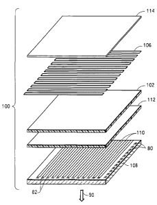
As shown in Fig. 2, each individual pixel of an organice electronic device
100 includes an electron injecting (cathode) contact 106 made from a
relatively
25 low work function metal (for example, Ca, Ba or alloys comprising Ca or Ba)
as
one electrode on the front of a photoactive organic material 102 deposited on
a
substrate 108 which has been partially coated with a layer of transparent
conducting material 110 with higher work function (high ionization potential)
to
serve as the second (transparent) electron-withdrawing (anode) electrode; i.e.
a
30 configuration that is well known for polymer LEDs (D. Braun and A.J.
Heeger,
Appl. Phys. Lett. 58, 1982 (1991). In accord with this invention, a layer 112
containing at least high resistivity layer of conductivity polymer such as
PANI(ES)
is interposed between the luminescent polymer layer 102 and the high work
function anode 110. Cathode 106 is electrically connected to contact pads 80,
and
35 anode 110 is electrically connected to contact pads 82. The layers 102,
106, 108,
110, and 112 are then isolated from the environment by a hermetic seal layer
114.
Upon application of electricity via contact pads 80, 82, which pads are
outside of
4
CA 02410535 2002-11-26
WO 01/99192 PCT/USO1/18189
the hermetic seal 70, light is emitted from the device in the direction shown
by
arrow 90.
The remainder of this description of preferred embodiments is organized
according to these various components. More specifically it contains the
s following sections:
The Photoactive Layer (102)
The Anode ( 110)
The High Resistivity Layer (112)
The Cathode (106)
l0 The Substrate (108)
Contact Pads (80, 90)
Other Optional Layers
Fabrication Techniques
Examples
15 The Photoactive Laver X102
Depending upon the application of the electronic device 100, the
photophotoactive layer 102 can be a light-emitting layer that is activated by
an
applied voltage (such as in a light-emitting diode or light-emitting
electrochemical
cell), a layer of material that responds to radiant energy and generates a
signal with
20 ~ or without an applied bias voltage (such as in a photodetector). Examples
of
photodetectors include photoconductive cells, photoresistors, photoswitches,
phototransistors, and phototubes, and photovoltaic cells, as these terms are
describe in Markus, John, Electronics and Nucleonics Dictionafy, 470 and 476
(McGraw-Hill, lnc. 1966).
25 Where the electronic device 100 is a light-emitting device, the photoactive
layer 102 will emit light when sufficient bias voltage is applied to the
electrical
contact layers. Suitable active light-emitting materials include organic
molecular
materials such asanthracene, butadienes, coumarin derivatives, acridine, and
stilbene derivatives, see, for example, Tang, U.S. Patent 4,356,429, Van Slyke
30 et al., U.S. Patent 4,539,507, the relevant portions of which are
incorporated
herein by reference. Alternatively, such materials can be polymeric materials
such
as those described in Friend et al. (IJ.S. Patent 5,247,190), Heeger et al.
(U.S.
Patent 5,408,109), Nakano et al. (IJ.S. Patent 5,317,169), the relevant
portions of
CA 02410535 2002-11-26
WO 01/99192 PCT/USO1/18189
which are incorporated herein by reference. The light-emitting materials may
be
dispersed in a matrix of another material, with and without additives, but
preferably form a layer alone. In preferred embodiments, the
electroluminescent
polymer comprises at least one conjugated polymer or a co-polymer which
contains segments of rc-conjugated moieties. Conjugated polymers are well
known
in the art (see, e.g., Conjugated Polymers, J.-L. Bredas and R. Silbey edt.,
Kluwer
Academic Press, Dordrecht, 1991). Representative classes of materials include,
but are not limited to the following:
(i) poly(p-phenylene vinylene) and its derivatives substituted at various
i0 positions on the phenylene moiety;
(ii) polyp-phenylene vinylene) and its derivatives substituted at various
positions on the vinylene moiety;
(iii) poly(arylene vinylene), where the arylene may be such moieties as
naphthalene, anthracene, furylene, thienylene, oxadiazole, and the like, or
one of
the moieties with functionalized substituents at various positions;
(iv) derivatives of poly(arylene vinylene), where. the arylene may be as in
(iii) above, substituted at various positions on the arylene moiety;
(v) derivatives of poly(arylene vinylene), where the arylene may be as in
(iii) above, substituted at various positions on the vinylene moiety;
(vi) co-polymers of arylene vinylene oligomers with non-conjugated
oligomers, and derivatives of such polymers substituted at various positions
on the
arylene moieties, derivatives of such polymers substituted at various
positions on
the vinylene moieties, and derivatives of such polymers substituted at various
positions on the arylene and the vinylene moieties;
(vii) polyp-phenylene) and its derivatives substituted at various positions
on the phenylene moiety, including ladder polymer derivatives such as poly(9,9-
dialkyl fluorene) and the like;
(viii) poly(arylenes) and their derivatives substituted at various positions
on the arylene moiety;
(ix) co-polymers of oligoarylenes with non-conjugated oligomers, and
derivatives of such polymers substituted at various positions on the arylene
moieties;
6
CA 02410535 2002-11-26
WO 01/99192 PCT/USO1/18189
(x) polyquinoline and its derivatives;
(xi) co-polymers of polyquinoline with p-phenylene and moieties having
solubilizing function;
(xii) rigid rod polymers such as poly(p-phenylene-2,6-benzobisthiazole),
poly(p-phenylene-2,6-benzobisoxazole), poly(p-phenylene-2,6-benzimidazole),
and their derivatives; and the like.
More specifically, the photoactive materials may include but are not
limited to poly(phenylenevinylene), PPV, and alkoxy derivatives of PPV, such
as
for example, poly(2-methoxy-5-(2'-ethyl-hexyloxy)-p-phenylenevinylene) or
to "MEH-PPV" (United States Patent No. 5,189,136). BCHA-PPV is also an
attractive active material. (C. Zhang, et al, J. Electron. Mater., 22, 413
(1993)).
PPPV is also suitable. (C. Zhang et al, Synth. Met., 62, 35 (1994) and
references
therein.) Luminescent conjugated polymer which are soluble in common organic
solvents are preferred since they enable relatively simple device fabrication
[A.
15 Heeger and D. Braun, U.S. Patent 5,408,109 and 5,869,350].
Even more preferred photoactive polymers and copolymers are the soluble
PPV materials described in H. Becker et al., Adv. Mater. 12, 42 (2000) and
referred to herein as C-PPV's. Blends of these and other semi-conducting
polymers and copolymers which exhibit electroluminescence can be used.
2o Where the electronic device 100 is a photodetector, the photophotoactive
layer 102 responds to radiant energy and produces a signal either with or
without
a biased voltage. Materials that respond to radiant energy and is capable of
generating a signal with a biased voltage (such as in the case of a
photoconductive
cells, photoresistors, photoswitches, phototransistors, phototubes) include,
for
25 example, many conjugated polymers and electroluminescent materials.
Materials
that respond to radiant energy and are capable of generating a signal without
a
biased voltage (such as in the case of a photoconductive cell or a
photovoltaic
cell) include materials that chemically react to light and thereby generate a
signal.
Such light-sensitive chemically reactive materials include for example, many
3o conjugated polymers and electro- and photo-luminescent materials. Specific
examples include, but are not limited to, MEH-PPV ("Optocoupler made from
semiconducting polymers", G. Yu, K. Pakbaz, and A. J. Heeger, .Iournal of
7
CA 02410535 2002-11-26
WO 01/99192 PCT/USO1/18189
Electrotaic Materials, Vol. 23, pp 925-928 (1994); and MEH-PPV Composites
with CN-PPV ("Efficient Photodiodes from Interpenetrating Polymer Networks",
J. J. M. Halls et al. (Cambridge group) Nature Vol. 376, pp. 498-500, 1995). .
The electroactive organic materials can be tailored to provide emission at
various
wavelengths.
In some embodiments, the polymeric photoactive material or organic
molecular photoactive material is present in the photophotoactive layer 102 in
admixture from 0% to 75% (w, basis overall mixture) of carrier organic
material
(polymeric or organic molecular). The criteria for the selection of the
carrier
organic material are as follows. The material should allow for the formation
of
mechanically coherent films, at low concentrations, and remain stable in
solvents
that are capable of dispersing, or dissolving the conjugated polymers for
forming
the film. Low concentrations of carrier materials are preferred in order to
minimize processing difficulties, i.e., excessively high viscosity or the
formation
of gross in homogeneities; however the concentration of the Garner should be
high
enough to allow for:formation of coherent structures. Where the Garner is a .
polymeric material, preferred Garner polymers are high molecular weight (M:W.
>
100,000) flexible chain polymers, such as polyethylene, isotactic
polypropylene,
polyethylene oxide, polystyrene, and the like. Under appropriate conditions,
which
2o can be readily determined by those skilled in the art, these macromolecular
materials enable the formation of coherent structures from a wide variety of
liquids, including water, acids, and numerous polar and non-polar organic
solvents. Films or sheets manufactured using these carrier polymers have
sufficient mechanical strength at polymer concentrations as low as 1 %, even
as
low as 0. 1%, by volume to enable the coating and subsequent processing as
desired. Examples of such coherent structures are those comprised of polyvinyl
alcohol), polyethylene oxide), poly-para (phenylene terephthalate),
poly-para-benzamide, etc., and other suitable polymers. On the other hand, if
the
blending of the final polymer cannot proceed in a polar environment, non-polar
3o carrier structures are selected, such as those containing polyethylene,
polypropylene, poly(butadiene), and the like.
8
CA 02410535 2002-11-26
WO 01/99192 PCT/USO1/18189
Typical film thicknesses of the photoactive layers range from a few
hundred l~ngstrom units (200 ~) to several thousand angstrom uiuts (10,000 ~)
(1 angstrom unit = 10-8 cm). Although the active film thicknesses are not
critical,
device performance can typically be improved by using thinner films. Preferred
thickness are from 3001 to 5,000 ~.
The Anode ( 11
In the device of the invention one electrode is transparent to enable light
emission from the device or light reception by the device. Most commonly, the
anode is the transparent electrode, although the present invention can also be
used
to in an embodiment where the cathode is the transparent electrode.
The anode 110 is preferably made of materials containing a metal, mixed
metal, alloy, metal oxide or mixed-metal oxide. Suitable metals include the
Group 11 metals, the metals in Groups 4, 5, and 6, and the Group 8-10
transition
metals. If the anode is to be light-transmitting, mixed-metal oxides of Groups
12,
' 13 and 14 metals, such as indium-tin-oxide; are generally used. The IUPAC
numbering system is used throughout, where the groups from the Periodic Table
are numbered from left to right as 1-18 (CRC Handbook of Chemistry and
Physics, 81 St Edition, 2000). The anode 110 may also comprise an organic
material such as polyaniline as described in "Flexible light-emitting diodes
made
2o from soluble conducting polymer," Nature vol. 357, pp 477-479 (11 June
1992).
Typical inorganic materials which serve as anodes include metals such as
aluminum, silver, platinum, gold, palladium, tungsten, indium, copper, iron,
nickel, zinc, lead and the like; metal oxides such as lead oxide, tin oxide,
indium/tin-oxide and the like; graphite; doped inorganic semiconductors such
as
silicon, germanium, gallium arsenide, and the like. When metals such as
aluminum, silver, platinum, gold, palladium, tungsten, indium, copper, iron,
nickel, zinc, lead and the like are used, the anode layer must be sufficiently
thin to
be semi-transparent. Metal oxides such as indium/tin-oxide are typically at
least
semitransparent.
3o As used herein, the term "transparent" is defined to mean "capable of
transmitting at least about 25%, and preferably at least about 50%, of the
amount
of light of a particular wavelength of interest". Thus a material is
considered
9
CA 02410535 2002-11-26
WO 01/99192 PCT/USO1/18189
"transparent" even if its ability to transmit light varies as a function of
wavelength
but does meet the 25% or SO% criteria at a given wavelength of interest. As is
known to those working in the field of thin films, one can achieve
considerable
degrees of transparency with metals if the layers are thin enough, for example
in
the case of silver and gold below about 300 A, and especially from about 20 A
to
about 250 A with silver having a relatively colorless (uniform) transmittance
and
gold tending to favor the transmission of yellow to red wavelengths.
The conductive metal-metal oxide mixtures can be transparent as well at
thicknesses up to as high as 2500 A in some cases. Preferably, the thicknesses
of
to metal-metal oxide (or dielectric) layers is from about 25 to about 1200 A
when
transparency is desired.
This layer is conductive and should be low resistance: preferably less than
300 ohms/square and more preferably less than 100 ohms/square.
The Buffer La, a
15 A high resistivity buffer layer 112 is placed between the layer of active
material 102 and anode 110..
This layer should be a high resistivity layer and shall comprise conductive
polyaniline (PANI) such as PANI(ES) or an equivalent conjugated conductive
polymer, most commonly in a blend with one or more nonconductive host
20 ' polymers. Suitable conductive polymers are usually doped polymers and may
include materials such as poly(ethylenedioxythiophene) "PEDT", polypyrolle,
polythiophene and PANI, all in their conductive forms. Polyaniline is
particularly
useful, particularly when it is in the emeraldine salt (ES) form. Useful
conductive
polyanilines include the homopolymer and derivatives usually as blends with
bulk
25 polymers. Examples of PANI are those disclosed in United States Patent
No. 5,232,631. The preferred PANI blend materials for this layer have a bulk
resistivity of greater than 104 ohms-cm. More preferred PANT blends have a
bulk
resistivity of greater than 105 ohms-cm.
When the terms "polyaniline" or PANI are used herein, they are used
30 generically to include substituted and unsubstituted materials, as well as
the other
equivalent conjugated conductive polymers such as polypyrrole or polythiophene
or PEDT, unless the context is clear that only the specific nonsubstituted
form is
intended. It is also used in a manner to include any accompanying dopants,
particularly acidic materials used to render the polyaniline conductive.
CA 02410535 2002-11-26
WO 01/99192 PCT/USO1/18189
In general, polyanilines are polymers and copolymers of film and
fiber-forming molecular weight derived from the polymerization of
unsubstituted
and substituted anilines of the Formula I:
Formula I
NH2
(R)n
(I~m
wherein
n is an integer from 0 to 4;
to m is an integer from 1 to 5 with the proviso that the sum of n and m is
equal to 5; and
R is independently selected so as to be the same or different at each
occurrence and is selected from the group consisting of alkyl, alkenyl,
alkoxy,
cycloalkyl, cycloalkenyl, alkanoyl, alkythio, aryloxy, alkylthioalkyl,
alkylaryl,
15 arylalkyl, amino, alkylamino, dialkylamino, aryl, alkylsulfinyl,
alkoxyalkyl,
alkylsulfonyl, arylthio, arylsulfinyl, alkoxycarbonyl, arylsulfonyl,
carboxylic acid,
halogen, cyano, or alkyl substituted with one or more sulfonic aid, carboxylic
acid,
halo, vitro, cyano or epoxy moieties; or carboxylic acid, halogen, vitro,
cyano, or
sulfonic acid moieties; or any two R groups together may form an alkylene or
2o alkenylene chain completing a 3, 4, 5, 6 or 7-membered aromatic or
alicyclic ring,
which ring may optionally include one or more divalent nitrogen, sulfur or
oxygen
atoms. Without intending to limit the scope of this invention, the size of the
various R groups ranges from about 1 carbon (in the case of alkyl) through 2
or
more carbons up through about 20 carbons with the total of n Rs being from
about
25 1 to about 40 carbons.
Illustrative of the polyanilines useful in the practice of this invention are
those of the Formula II to V:
11
CA 02410535 2002-11-26
WO 01/99192 PCT/USO1/18189
~)n
a NH ~ ~ NH
X ~ llllm ~ Z
or
ll')n
III ~ ~ ~ NH
~m Z
or
~)n
H
N ~ ~ N ~ ~ N
--~--~ ~ ,
x ~m
y z
or
~)n
N- N
X ~m
y z
1 o wherein:
n, m and R are as described above except that m is reduced by 1 as a
hydrogen is replaced with a covalent bond in the polymerization and the sum of
n
plus m equals 4;
12
CA 02410535 2002-11-26
WO 01/99192 PCT/USO1/18189
y is an integer equal to or greater than 0;
x is an integer equal to or greater than 1, with the proviso that the sum of x
and y is greater than 1; and
z is an integer equal to or greater than 1.
The following listing of substituted and unsubstituted anilines axe
illustrative of those which can be used to prepare polyanilines useful in the
practice of this invention.
Aniline 2,5-Dimethylaniline
o-Toluidine 2,3-Dimethylaniline
to m-Toluidine 2,5-Dibutylaniline
o-Ethylaniline 2,5-Dimethoxyaniline
m-EIthylanilin Tetrahydronaphthylamine
o-Ethoxyaniline o-Cyanoaniline
m-Butylaniline 2-Thiomethylaniline
i5 m-Hexylaniline 2,5-Dichloroaniline
m-Octylaniline 3-(n-Butanesulfonic acid)aniline
4-Bromoaniline
2-Bromoaniline
3-Bromoaniline 2,4-Dimethoxyaniline
20 3-Acetamidoaniline 4-Mercaptoaniline
4-Acetamidoaniline 4-Methylthioaniline
5-Chloro-2-methoxyaniline 3-Phenoxyaniline
5-Chloro-2-ethoxyaniline 4-Phenoxyaniline
25 Illustrative of useful R groups are alkyl, such as methyl, ethyl, octyl,
nonyl,
tert-butyl, neopentyl, isopropyl, sec-butyl, dodecyl and the like, alkenyl
such as
1-propenyl, 1-butenyl, 1-pentenyl, 1-hexenyl, 1-heptenyl, 1-octenyl and the
like;
alkoxy such as propoxy, butoxy, methoxy, isopropoxy, pentoxy, nonoxy, ethoxy,
octoxy, and the like, cycloalkenyl such as cyclohexenyl, cyclopentenyl and the
30 like; alkanoyl such as butanoyl, pentanoyl, octanoyl, ethanoyl, propanoyl
and the
like; alkylsulfinyl, alkysulfonyl, alkylthio, arylsulfonyl, arylsulfinyl, and
the like,
such as butylthio, neopentylthio, methylsulfinyl, benzylsulfinyl,
phenylsulfmyl,
propylthio, octylthio, nonylsulfonyl, octylsulfonyl, methylthio,
isopropylthio,
phenylsulfonyl, methylsulfonyl, nonylthio, phenylthio, ethylthio, benzylthio,
35 phenethylthio, naphthylthio and the like; alkoxycarbonyl such as
methoxycarbonyl, ethoxycarbonyl, butoxycarbonyl and the like, cycloalkyl such
as
cyclohexyl, cyclopentyl, cyclooctyl, cycloheptyl and the like; alkoxyalkyl
such as
methoxymethyl, ethoxymethyl, butoxymethyl, propoxyethyl, pentoxybutyl and the
13
CA 02410535 2002-11-26
WO 01/99192 PCT/USO1/18189
like; aryloxyalkyl and aryloxyaryl such as phenoxyphenyl, phenoxymethylene and
the like; and various substituted alkyl and aryl groups such as 1-
hydroxybutyl,
1-aminobutyl, 1-hydroxylpropyl, 1-hydyroxypentyl, 1-hydroxyoctyl,
1-hydroxyethyl, 2-nitroethyl, trifluoromethyl, 3,4-epoxybutyl, cyanomethyl,
3-chloropropyl, 4-nitrophenyl, 3-cyanophenyl, and the like; sulfonic acid
terminated alkyl and aryl groups and carboxylic acid terminated alkyl and aryl
groups such as ethylsulfonic acid, propylsulfonic acid, butylsulfonic acid,
phenylsulfonic acid, and the corresponding carboxylic acids.
Also illustrative of useful R groups are divalent moieties formed from any
1o two R groups such as moieties of the formula:
-(CH2)-n*
wherein n* is an integer from about 3 to about 7, as for example -(CH2)-4,
-(CH2)-3 and -(CH2)-5, or such moieties which optionally include heteroatoms
of
oxygen and sulfur such as -CH2SCH2- and -CH2-O-CH2-. Exemplary of other
useful R groups are divalent alkenylene chains including 1 to about 3
conjugated
double bond unsaturation such as divalent 1,3-butadiene and like moieties.
Preferred for use in the practice of this invention are polyanilines of the
2o above Formulas II to V in which:
n is an integer from 0 to about 2;
m is an integer from 2 to 4, with the proviso that the sum of n and m is
equal to 4;
R is alkyl or alkoxy having from 1 to about 12 carbon atoms, cyano,
halogen, or alkyl substituted with carboxylic acid or sulfonic acid
substituents;
x is an integer equal to or greater than l;
y is an integer equal to or greater than 0, with the proviso that the sum of x
and y is greater than about 4, and
z is an integer equal to or greater than about 5.
3o In more preferred embodiments of this invention, the polyaniline is derived
from unsubstituted aniline, i.e., where n is 0 and m is 5 (monomer) or 4
(polymer).
In general, the number of monomer repeat units is at least about 50.
As described in United States Patent Number 5,232,631, the polyaniline is
rendered conductive by the presence of an oxidative or acidic species. Acidic
species and particularly "functionalized protonic acids" are preferred in this
role.
A "functionalized protonic acid" is one in which the counter-ion has been
functionalized preferably to be compatible with the other components of this
layer.
14
CA 02410535 2002-11-26
WO 01/99192 PCT/USO1/18189
As used herein, a "protonic acid" is an acid that protonates the polyaniline
to form
a complex with said polyaniline.
In general, functionalized protonic acids for use in the invention are those
of Formulas VI and VIIa
or
A-R IV
R'n
A
VII
wherein:
A is sulfonic acid, selenic acid, phosphoric acid, boric acid or a carboxylic
acid group; or hydrogen sulfate, hydrogen selenate, hydrogen phosphate;
n is an integer from 1 to 5;
R is alkyl, alkenyl, alkoxy, alkanoyl, alkylthio, alkylthioalkyl, having from
1 to about 20 carbon atoms; or alkylaryl, arylalkyl, alkylsulfinyl,
alkoxyalkyl,
alkylsulfonyl, alkoxycarbonyl, carboxylic acid, where the alkyl or alkoxy has
from
0 to about 20 carbon atoms; or alkyl having from 3 to about 20 carbon atoms
substituted with one or more sulfonic acid, carboxylic acid, halogen, nitro,
cyano,
2o diazo, or epoxy moieties; or a substituted or unsubstituted 3, 4, 5, 6 or
7 membered aromatic or alicyclic carbon ring, which ring may include one or
more divalent heteroatoms of nitrogen, sulfur, sulfinyl, sulfonyl or oxygen
such as
thiophenyl, pyrolyl, furanyl, pyridinyl.
In addition to these monomeric acid forms, R can be a polymeric backbone
from which depend a plurality of acid functions "A." Examples of polymeric
acids include sulfonated polystyrene, sulfonated polyethylene and the like. In
these cases the polymer backbone can be selected either to enhance solubility
in
nonpolar substrates or be soluble in more highly polar substrates in which
materials such as polymers, polyacrylic acid or poly(vinylsulfonate), or the
like,
3o can be used.
CA 02410535 2002-11-26
WO 01/99192 PCT/USO1/18189
R' is the same or different at each occurrence and is alkyl, alkenyl, alkoxy,
cycloalkyl, cycloalkenyl, alkanoyl, alkylthio, aryloxy, alkylthioalkyl,
alkylaryl,
arylalkyl, alkylsulfinyl, alkoxyalkyl, alkylsulfonyl, aryl, arylthio,
arylsulfinyl,
alkoxycarbonyl, arylsulfonyl, carboxylic acid, halogen, cyano, or alkyl
substituted
with one or more sulfonic acid, carboxylic acid, halogen, nitro, cyano, diazo
or
epoxy moieties; or any two R substituents taken together are an alkylene or
alkenylene group completing a 3, 4, 5, 6 or 7 membered aromatic or alicyclic
carbon ring or multiples thereof, which ring or rings may include one or more
divalent heteroatoms of nitrogen, sulfur, sulfinyl, sulfonyl or oxygen. R'
typically
1 o has from about 1 to about 20 carbons especially 3 to 20 and more
especially from
about g to 20 carbons.
Materials of the above Formulas VI and VII are preferred in which:
A is sulfonic acid, phosphoric acid or carboxylic acid;
n is an integer from 1 to 3;
is R is alkyl, alkenyl, alkoxy, having from 6 to about 14 carbon atoms; or
arylalkyl, where the alkyl or alkyl portion or alkoxy has from 4 to about 14
carbon
atoms; or alkyl having from 6 to about 14 carbon atoms substituted with one or
more, carboxylic acid, halogen, diazo, or epoxy moieties;
R' is the same or different at each occurrence and is alkyl, alkoxy,
2o alkylsulfonyl, having from 4 to 14 carbon atoms, or alkyl substituted with
one or
more halogen moieties again with from 4 to 14 carbons in the alkyl.
Among the particularly preferred embodiments, most preferred for use in
the practice of this invention are functionalized protonic acids of the above
Formulas VI and VII in which:
25 A is sulfonic acid;
n is the integer 1 or 2;
R is alkyl or alkoxy, having from 6 to about 14 carbon atoms; or alkyl
having from 6 to about 14 carbon atoms substituted with one or more halogen
moieties;
3o R' is alkyl or alkoxy, having from 4 to 14, especially 12 carbon atoms, or
alkyl substituted with one or more halogen, moieties.
16
CA 02410535 2002-11-26
WO 01/99192 PCT/USO1/18189
Preferred functionalized protonic acids are organic sulfonic acids such as
dodecylbenzene sulfonic acid and more preferably
poly(2-acrylamido-2-methyl-1-propanesulfonic acid) ("PAAMPSA").
The amount of functionalized protonic acid employed can vary depending
on the degree of conductivity required. In general, sufficient functionalized
protonic acid is added to the polyaniline-containing admixture to form a
conducting material. Usually the amount of functionalized protonic acid
employed is at least sufficient to give a conductive polymer (either in
solution or
in solid form).
l0 The polyaniline can be conveniently used in the practice of this invention
in any of its physical forms. Illustrative of useful forms are those described
in
Green, A.G., and Woodhead, A. E., J. Chem. Soc., 101, 1117 (1912) and
I~obayashi, et al., J. Electroanl. ChenZ., 177, 281-91 (1984), which are
hereby
incorporated by reference. For unsubstituted polyaniline, useful forms include
leucoemeraldine, protoemeraldine, emeraldine, nigraniline and
tolu-protoemeraldine forms, with the emeraldine form being preferred.
Copending United States Patent Application Serial No. 60/168,856 of Cao,
Y. and Zhang, C. discloses the formation of low conductivity blends of
conjugated
polymers with non-conductive polymers and is incorporated herein by reference.
The particular bulk polymer or polymers added to the conjugated polymer
can vary. The selection of materials can be based upon the nature of the
conductive polymer, the method used to blend the polymers and the method used
to deposit the layer in the device.
The materials can be blended by dispersing one polymer in the other, either
as a dispersion of small particles or as a solution of one polymer in the
other. The
polymer are typically admixed in a fluid phase and the layer is typically laid
out of
a fluid phase.
We have had our best results using water-soluble or Water-dispensable
conjugated polymers together with water-soluble or water-dispensable bulk
polymers. In this case, the blend can be formed by dissolving or dispersing
the
two polymers in water and casting a layer from the solution or dispersion.
17
CA 02410535 2002-11-26
WO 01/99192 PCT/USO1/18189
Organic solvents can be used with organic-soluble or organic dispensable
conjugated polymers and bulk polymers. In addition, blends can be formed using
melts of the two polymers or by using a liquid prepolymer or monomer form of
the bulk polymer which is subsequently polymerized or cured into the desired
final material.
In those presently preferred cases where the PANI is water-soluble or
water dispersible and it is desired to cast the PAIVI layer from an aqueous
solution, the bulk polymer should be water soluble or water dispersible. In
such
cases, it is selected from, for example polyacrylamides (PAM), poly(acrylic
acid )
(PAA) polyvinyl pyrrolidone) (PVPd), acrylamide copolymers, cellulose
derivatives, carboxyvinyl polymer, polyethylene glycols), polyethylene oxide)
(PEO), polyvinyl alcohol) (PVA), polyvinyl methyl ether), polyamines,
polyimines, polyvinylpyridines; polysaccharides, and polyurethane dispersions.
In the case where it is desired to cast the layer from a non-aqueous solution
or dispersion the bulk polymer may be selected from, for example liquefiable
polyethylenes, isotactic polypropylene, polystyrene, poly(vinylalcohol),
poly(ethylvinylacetate), polybutadienes, polyisoprenes,
' ethylenevinylene-copolymers, ethylene-propylene copolymers,
poly(ethyleneterephthalate); poly(butyleneterephthalate) and nylons such as
2o nylon 12, nylon 8, nylon 6, nylon 6.6 and the like, polyester materials,
polyamides
such as polyacrylamides and the like.
In those cases where one polymer is being dispersed in the other, the
common solubility of the various polymers may not be required.
The relative proportions of the polyaniline and bulk polymer or
prepolymer can vary. For each part of polyaniline there can be from 0 to as
much
as 20 parts by weight of bulk polymer or prepolymer with 0.5 to 10 and
especially
1 to 4 parts of bulk material being present for each part of PANI.
Solvents for the materials used to cast this layer are selected to compliment
the properties of the polymers.
3o In the preferred systems, the PANI and bulk polymer are both
water-soluble or water-dispersible and the solvent system is an aqueous
solvent
system such as water or a mixture of water with one or more polar organic
18
CA 02410535 2002-11-26
WO 01/99192 PCT/USO1/18189
materials such as lower oxyhydrocarbons for example lower alcohols, ketones
and
esters.
These materials include, without limitation, water mixed with methanol,
ethanol, isopropanol, acetone methyl ethyl ketone and the like.
If desired, but generally not preferred, a solvent system of polar organic
liquids could be used.
In the case of conducting polymers such as PAIVI and bulk polymers which
are not water-soluble or water-dispersible, nonpolar solvents are most
conunonly
used.
to Illustrative of useful common nonpolar solvents are the following
materials: substituted or unsubstituted aromatic hydrocarbons such as benzene,
toluene, p-xylene, m-xylene, naphthalene, ethylbenzene, styrene, aniline and
the
like; higher alkanes such as pentane, hexane, heptane, octane, nonane, decane
and
the like; cyclic alkanes such as decahydronaphthalene; halogenated alkanes
such
as chloroform, bromoform, dichloromethane and the like; halogenated aromatic
hydrocarbons such as chlorobenzene, o-dichlorobenzene, m-dichlorobenzene,
p-dichlorobenzene and the like; higher alcohols such as 2-butanol, 1-butanol,
hexanol, pentanol, decanol, 2-methyl-1-propanol and the like; higher ketones
such
as hexanone, butanone, pentanone and the like; heterocyclics such as
morpholine;
2o perfluorinated hydrocarbons such as perfluorodecaline, perfluorobenzene and
the
like.
The thickness of the conjugated polymer layer will be chosen with the
properties of the diode in mind. In those situations where the composite anode
is
to be transparent, it is generally preferable to have the layer of PANI as
thin as
practically possible bearing in mind the failure problem noted in Fig. 1.
Typical
thicl~iesses range from about 100 ~ to about 50001. When transparency is
desired, thicknesses of from about 100 ~ to about 30001 are preferred and
especially about 2000 ~.
With a film thickness of 200 nm or greater, the electrical resistivity of the
3o PAIVI(ES) blend layer should be greater than or equal to 104 ohm-cm to
avoid
cross talk and inter-pixel current leakage. Values in excess of 105 ohm-cm are
preferred. Even at 105 ohm-cm, there is some residual current leakage and
19
CA 02410535 2002-11-26
WO 01/99192 PCT/USO1/18189
consequently some reduction in device efficiency. Thus, values of
approximately
105 to 108 ohm-cm are even more preferred. Values greater than 109 ohm-cm will
lead to a significant voltage drop across the injection/buffer layer and
therefore
should be avoided.
The Cathode (106)
Suitable materials for use as cathode materials are any metal or nonmetal
having a lower work function than the first electrical contact layer (in this
case, an
anode). Materials for the cathode layer 106 (in this case the second
electrical
contact) can be selected from alkali metals of Group 1 (e.g., Li, Cs), the
Group 2
l0 (alkaline earth) metals - - commonly calcium, barium, strontium, the Group
12
metals, the rare earths - commonly ytterbium, the lanthanides, and the
actinides.
Materials such as aluminum, indium and copper, silver, combinations thereof
and
combinations with calcium and/or barium, Li, magnesium, LiF can be used.
. Alloys of low work function metals, such as for example alloys of
magnesium in silver and alloys of lithium in aluminum, are also useful. The
thickness of the electron-injecting cathode layer ranges from less than 15 ~
to as
much as 5,0001. This cathode layer 106 can be patterned to give a pixellated
aiTay or it can be continuous and overlaid with a layer of bulk conductor such
as
silver, copper or preferably aluminum which is, itself, patterned.
. The cathode layer may additionally include a second layer of a second
metal added to give mechanical strength and durability.
The Substrate (108)
In most embodiments, the diodes are prepared on a substrate. Typically the
substrate should be nonconducting. In those embodiments in which light passes
through it, it is transparent. It can be a rigid material such as a rigid
plastic
including rigid acrylates, carbonates, and the like, rigid inorganic oxides
such as
glass, quartz, sapphire, and the like. It can also be a flexible transparent
organic
polymer such as polyester - for example poly(ethyleneterephthalate), flexible
polycarbonate, poly (methyl methacrylate), polystyrene) and the like.
The thickness of this substrate is not critical.
CA 02410535 2002-11-26
WO 01/99192 PCT/USO1/18189
Contact Pads (80, 82)
Any contact pads 80, 82 useful to connect the electrode of the device 100
to the power source (not shown) can be used, including, for example,
conductive
metals such as gold (Au), silver (Ag), nickel (Ni), copper (Cu) or aluminum
(Al).
Preferably, contact pads 80, 82 have a height (not shown) projected beyond
the thickness of the high work function electrode lines 110 below the total
thickness of layer.
Preferably, the dimensions of layers 102, 110, and 112 are such that
contacts pads 80 are positioned on a section of the substrate 108 not covered
by
1o layers 102, 112 and 114. In addition, the dimensions of layer 106, 102,
110, and
112 are such that the entire length and width electrode lines 106 and
electrode
lines 110 have at least one layer 102, 112 intervening between the electrodes
106,
110, while electrical connection can be made between electrode 106 and contact
pads 80.
' 15
Other Optional Layers (not shown)
An optional layer including an electron injection/transport material may
be provided between the photoactive layer 102 and the cathode 106. This
optional
layer can function both to facilitate electron injectionltransport, and also
serve as a
2o buffer layer or confinement layer to prevent quenching reactions at layer
interfaces. Preferably, this layer promotes electron mobility and reduces
quenching reactions. Examples of electron transport materials for optional
layer
include metal chelated oxinoid compounds, such as
tris(8-hydroxyquinolato)aluminum (Alq3); phenanthroline-based compounds,
25 such as 2,9-dimethyl-4,7-diphenyl-1,10-phenanthroline (DDPA) or 4,7-
diphenyl-
1,10-phenanthroline (DPA), and azole compounds such as 2-(4-biphenylyl)-5-(4-t-
butylphenyl)-1,3,4-oxadiazole (PBD) and 3-(4-biphenylyl)-4-phenyl-5-(4-t-
butylphenyl)-1,2,4-triazole (TAZ), polymers containing DDPA, DPA, PBD, and
TAZ moiety and polymer blends thereof, polymer blends containing containing
3o DDPA, DPA, PBD, and TAZ.
It is known to have other layers in organic electronic devices. For
example, there can be a layer (not shown) between the buffer layer 112 and the
21
CA 02410535 2002-11-26
WO 01/99192 PCT/USO1/18189
photphotoactive layer 102 to facilitate positive charge transport and/or band-
gap
matching of the layers, or to function as a protective layer, or to improve
the
interfacial property. Similarly, there can be additional layers (not shown)
between
the photoactive layer 102 and the cathode layer 106 to facilitate negative
charge
transport and/or band-gap matching between the layers, or to function as a
protective layer. Layers that are known in the art can be used. In addition,
any of
the above-described layers can be made of two or more layers. Alternatively,
some or all of anode layer 110, the buffer layer 112 the photophotoactive
layer
102, and cathode layer 106, may be surface treated to increase charge carrier
l0 transport efficiency. The choice of materials for each of the component
layers is
preferably determined by balancing the goals of providing a device with high
device efficiency.
Fabrication Techniques
i5 The various elements of the devices of the present invention may be
fabricated by any of the techniques well known in the art, such as solution
casting,
screen printing, web coating, ink jet printing, sputtering, evaporation,
precursor
polymer processing, melt-processing, and the like, or any combination thereof.
In
the most common approach, the diodes are built up by sequential deposit of
layers
20 upon a substrate. In a representative preparation, the inorganic contact
110
portion of the composite electrode is laid down first. This layer is commonly
deposited by vacuum sputtering (RF or Magnetron), electron beam evaporation,
thermal vapor deposition, chemical deposition or the like methods commonly
used
to form inorganic layers.
25 Next, the buffer layer 112 is laid down. This layer is usually most
conveniently deposited as a layer from solution by spin casting or like
technique.
In those preferred cases where the layer is formed from water-soluble or
water-dispersible material water is generally used as the spin-casting medium.
In
cases where a non-aqueous solvent is called for are used such as toluene,
xylenes,
30 styrene, aniline, decahydronaphthalene, chloroform, dichloromethane,
chlorobenzenes and morpholine.
22
CA 02410535 2002-11-26
WO 01/99192 PCT/USO1/18189
Next, the photoactive layer 102 of conjugated polymer is deposited. The
conjugated polymer can be deposited or cast directly from solution. The
solvent
employed is one which will dissolve the polymer and not interfere with its
subsequent deposition. Depending upon the active polymer used the solvent can
be non-aqueous or aqueous.
Typically, non-aqueous solvents include halohydrocarbons such as
methylene chloride, chloroform, and carbon tetrachloride, aromatic
hydrocarbons
such as xylene, benzene, toluene, other hydrocarbons such as decaline, and the
like. Mixed solvents can be used, as well. Polar solvents such as water,
acetone,
acids and the like may be suitable. These are merely a representative
exemplification and the solvent can be selected broadly from materials meeting
the criteria set forth above.
When depositing various polymers on a substrate, the solution can be
relatively dilute, such as from 0.1 to 20% w in concentration, especially 0.2
to
5% w. Film thicknesses of 500-4000 and especially 1000-2000 ~ are typically
used.
Finally the low work function electron-injecting contact is added. This
contact is typically vacuum evaporated onto the top surface of the active
polymer
layer.
2o These steps can be altered and even reversed if an "upside down" diode is
desired, so that the cathode, rather than the anode, is the transparent
electrode.
It will also be appreciated that the structures just described and their
fabrication can be altered to include other layers for physical strength and
protection, to alter the color of the light emission or sensitivity of the
diodes or the
2s like.
The invention is based on the development of formulations of conductive
conjugated polymers such as the emraldine salt (ES) of polyaniline, PANI(ES),
which leads to high resistivity films for use in high efficiency pixelated
polymer
electronic devices such as emissive displays and a method has been developed
for
3o casting transparent thin films of the high resistivity conductive polymers
onto
pre-patterned ITO substrates. In addition, a method has been developed for
depositing a thin transparent film of high resisitivity materials such as
PAIVI(ES)
23
CA 02410535 2002-11-26
WO 01/99192 PCT/USO1/18189
from an aqueous dispersion onto a either pre-patterned ITO-on-glass substrates
or
ITO-on-plastic substrates. By using the high resistivity layer described in
this
invention, longer operating life is enabled in high information content
displays
without the need for registered patterning of the high resistivity layer
The invention will be further described by the following Examples which
are presented to illustrate the invention but not to limit its scope.
Unless otherwise specified all percentages are percentages by weight.
EXAMPLES
EXAMPLE 1
PANI-PAAMPSA was prepared using a procedure similar to that
described in the reference Y. Cao, et al, Polymer, 30(1989) 2305, more
specifically, as described below. HCl in this reference was replaced by
poly(2-acrylamido-2-methyl-1-propanesulfonic acid (PAAMPSA) (available from
Aldrich, Milwaukee, WI 53201).
The emeraldine salt (ES) form was verified by the typical green color.
First, 30.5 g (0.022 mole) of 15% PAAMPSA in water (Aldrich ) was diluted to
2.3% by adding 170 ml water. While.stirring, 2.2 g (0.022M) aniline was added
into the PAAMPSA solution. Then, 2.01 g (0.0088M) of ammonium persulfate in
10 ml water was added slowly into the aniline/PAAMPSA solution under
vigorous stirring. The reaction mixture was stirred for 24 hours at room
temperature. To precipitate the product, PANT-PAAMPSA, 1000 ml of acetone
was added into reaction mixture. Most of acetone/water was decanted and then
the PANI-PAAMPSA precipitate was filtered. The resulting gum-like product
was washed several times by acetone and dried at 40°C under dynamic
vacuum for
24 hours.
This Example demonstrates the direct synthesis of PANI-PAAMPSA.
EXAMPLE 2
One gram (1.0 g) of the PANI-PAAMPSA powder as prepared in
Example 1 was mixed with 100 g of deionized water in a plastic bottle. The
mixture was rotated at room temperature for 48 hours. The
solutions/dispersions
were then filtered through 0.45 ~,m polypropylene filters. Different
concentrations
24
CA 02410535 2002-11-26
WO 01/99192 PCT/USO1/18189
of PANI-PAAMPSA in water are routinely prepared by changing the quantity of
PA1VI-PAAMPSA mixed into the water.
This Example demonstrates that PANI-PAAMPSA can be
dissolved/dispersed in water and subsequently filtered through a 0.45 ~,m
filter.
EXAMPLE 3
A PAIVI-PAAMPSA film was drop-casted from 1 % w/w)
solution/dispersion in water. The film thickness was measured to be 650 nm by
a
surface profilometer (Alpha-Step 500) (available from KLA-Tencor, San Jose, CA
95134). Using standard X-ray equipment, a wide-angle diffraction diagram
l0 (WARD) was taken on the PATH-PAAMPSA film. The diffraction pattern
showed no characteristic diffraction peaks; the data indicated that the film
was
amorphous.
This Example demonstrates that the PA1VI-PAAMPSA film cast from
water is amorphous (crystallinity less than 10%).
EXAMPLE 4
Four grams (4.0 g) of polyacrylamide (PAM) (M.W. 5,000,000 -
6,000,000, available from Polysciences (Warrinton, PA 18976) was mixed with
400 ml deionized water in a plastic bottle. The mixture was rotated at room
temperature for at least 48 hours: The solution/dispersion was then filtered
2o through 1 ~,m polypropylene filters. Different concentrations of PAM are
routinely prepared by changing the quantity of PAM dissolved.
This Example demonstrates that PAM can be dissolved/dispersed in water
and subsequently filtered through a 1 ~m filter.
EXAMPLE 5
Ten grams (10 g) of the PAIVI-PAAMPSA solution as prepared in
Example 2 was mixed with 20 g of 1% (w/w) PAM solution as prepared in
Example 4 (mixed at room temperature for 24 hours). The solution was then
filtered through 0.45 wm polypropylene filters. The PANI-PAAMPSA to PAM
ratio was 1:2 in the blend solution. Different blend ratios of the PAI~II-
3o PAAMPSA/PAM solutions were prepared by changing the concentrations of
PANI-PAAMPSA and PAM in the starting solutions including the following:
PAIVI-PAAMPSA/PAM (w/w) at 2/1, and 1/1.
CA 02410535 2002-11-26
WO 01/99192 PCT/USO1/18189
This Example demonstrates that PANI-PAAMPSA/PAM blends can be
prepared with a range of PAM concentrations, that these blends can be
dissolved/dispersed in water and that they can be filtered through a 0.45 Vim.
EXAMPLE 6
Example 5 was repeated, but PAAMPSA was used instead of PAM. The
blend ratio of PANI-PAAMPSA/PAAMPSA (w/w) was, respectively, l/0.1, 1/0.3,
1/0.5, 1/1 and 1/2.
This Example demonstrates that PA1VI-PAAMPSA/PAAMPSA blends can
be prepared with a range of PAAMPSA concentrations, that these blends can be
to dissolved/dispersed in water and that they can be filtered through a 0.45
~m filter.
EXAMPLE 7
Example 5 was repeated, but PEO was used instead of PAM. The blend
ratio of PANI-PAAMPSA/PEO (w/w) was 1/1.
EXAMPLE 8
Glass substrates were prepared with patterned ITO electrodes. Using the
blend solutions as prepared in Examples 5, 6 and 7, polyaniline blend layers
were
spin-cast on top of the patterned substrates and thereafter, baked at 90
°C in a
vacuum oven for 0.5 hour. The.resistance between ITO electrodes was measured
using a high resistance I~eithley 487 Picoammeter, from Keithley Instruments
Inc.;
(Cleveland, Ohio 44139). Table 1 shows the conductivity of PAIVI(ES)-blend
films with different blend compositions. As can be seen from Table, the
conductivity can be controlled over a wide range.
This Example demonstrates that the PAIVI-PAAMPSA blends can be
prepared with bulk conductivities less than 10'4 S/cm, and even less than 10-
5'
S/cm; i.e. sufficiently low that interpixel current leakage can be limited
without
need for patterning the PA1VI-PAAMPSA blend film.
26
CA 02410535 2002-11-26
WO 01/99192 PCT/USO1/18189
Table 1.
Surface resistivity and bulk conductivity of PAIVI-PAAMPSA blends
Blend host polymerThickness A/B ratio*Surface Electrical
(B) (A) (w/w) ResistanceConductivityResistivity
(if present) (ohm/sq)(S/cm) (ohm-cm)**
100 none 350 1.2x10⁸ 2.3x10⁻³ 4.3x10²
1 O 1 none 200 2.2x 2.2x 10-3 4.5 x
1 O8 1 Oz
102 PAM 300 211 2.3x10⁹ l.SxlO-a 6.7 x10³
103 PAM 230 2I1 5.3x10⁹ 8.2x10⁻⁵ 1.2x10
104 PAM 510 1/1 8.2x10⁹ 2.3x10⁻⁵ 4.3 x10⁴
105 PAM 264 111 2.0x10' 1.9x10⁻⁵ 5.3 x10⁴
106 PAM 220 1/1 2.2x10' 2,1x10⁻⁵ 4.8 x10
107 PAM 285 1/2 1.4x10" 2.5x10⁻⁶ 4 x10⁵
108 PAAMPSA 260 1/0.1 2.4x10⁹ 1.6x10- 6.3 x10³
109 PAAMPSA 350 1/0.3 9.2x10⁹ 4.6x10- 2.2 x10³
110 PAAMPSA 230 1/0.5 4.5x10$ 9.5x10⁻⁴ 1.1 x10³
111 PAAMPSA 630 1/0.5 3.7x10⁸ 4.3x10⁻⁴ 2.3 x10³
112 PAAMPSA 920 1/0.5 6.8x10' 1.6x10⁻⁴ 6.3 x10³
113 PAAMPSA 950 1/1 2.8x10⁸ 3.8x10 2.6 x10³
114 PAAMPSA 1280 1/1 6.7x10' 1.2x10⁻³ 8.3 x10²
115 PAAMPSA 1740 1/2 2.5x10⁸ 2.3x10⁻⁴ 4.3 x10³.
116 PAAMPSA 3060 1/2 8.4x10' 3.9x10⁻⁴ 2.6 x10³
117 PEO 250 1/1 3.0x10⁹ 1.3x10⁴ 7.7 x10³
* A being
PAlVI-PAAMPSA
** trical (i.e.;
Elec Resistanceinverse
of conductivity)
EXAMPLE 9
20 g of a PANI-PAAMPSA solution as prepared in Example 2 was mixed
(at room temperature for 12 days) with 10 g of 1 wt% PAM solution as prepared
l0 in Example 4 and 2.0 g of 15% PAAMPSA solution (available from Aldrich) The
solution was then filtered through 0.45 ~,m polypropylene filters. The content
of
PAIVI-PAAMPSA in the blend solution was 33wt% Different blend ratios of the
PAIVI-PAAMPSA : PAAMPSA : PAM blend solutions are prepared by changing
the concentrations in the starting solutions.
EXAMPLE 10
Example 9 was repeated; the content of PAI\TI-PAAMPSA is kept at
33wt%, but the ratio of host polymers PAAMPSAIPAM (w/w) was changed to
2/0, 0.5/1, 1/1 and 0/2, respectively.
EXAMPLE 11
30 g of a solution as prepared in Example 2 was mixed with 15 g of
deionized water and 0.6 g of PAM (M.W. 5,000,000 - 6,000,000, available from
27
CA 02410535 2002-11-26
WO 01/99192 PCT/USO1/18189
Polysciences) under stirnng at room temperature for 4 - 5 days. The ratio of
PANI-PAAMPSA to PAM in the blend solution was 1/2. Blend solutions were
also prepared in which the content of PANI-PAAMPSA was 0, 10, 25 and 40%,
respectively.
EXAMPLE 12
The resistance measurements of Example 8 were repeated, but the
PA1VI(ES) layer was spin-cast from the blend solutions prepared in Examples
11.
Fig. 3 shows the conductivity of PANI(ES)-blend films with different blend
compositions. As can be seen from the data, the conductivity can be controlled
in
to wide range to meet display requirements. Conductivity values less than 10-5
S/cm
(electrical resistivity of greater than 10~ ohm-cm). can be obtained. With
higher
concentrations of PAM in the blend, the conductivity dropped below 10-6 S/cm
(electrical resistivity of greater than 106 ohm-cm). .
This Example demonstrates that PANI(ES)-blend films can be prepared
15 with conducitivities less than 10-5 Slcm and even less than 10-6 S/cm.
EXAMPLE 13
The resistance measurements of Example 8 were repeated, but the
PAhII(ES) layer was spin-cast from the blend solutions as prepared in Examples
9
and 10. Table 2 shows the conductivity of polyblend films with different blend
2o compositions; the conductivity can be controlled over a wide range of
values.
This Example demonstrates that the PANI-PAAMPSA blends using
PAAMPSA/PAM as host polymers can be prepared with bulk conductivities less
than 10-5 S/cm, even less than 10-6 S/cm and for specific formulations less
than
10-' S/cm. The conductivities of the PANI(ES) blends are sufficiently low that
25 interpixel current leakage can be limited without need for patterning the
blend
film.
28
CA 02410535 2002-11-26
WO 01/99192 PCT/USO1/18189
Table 2. Bulls ans surface resistance for PAIVI(ES) blends with different
compositions and
thickness
Ratio of host polymers* Thickness Rohm)** ohm/sq Conductivity Resistivity
PAAMPS/PAM (A) (S/cm) (ohm-cm)
1.5/0.5 2100 9.8x10⁶ 5.2x10$ 9.0x10⁻⁵ 1.1x10
1000 1.0x10⁸ 5.3x10⁹ 1.9x10⁻⁵ 5.3x10
l0 2/0 2080 1.6x10' 8.5x10⁸ 5.6x10⁻⁵ 1.8x10⁴
1300 3.9x10⁷ 2.1x10⁹ 3.7x10⁻⁵ 2.7x10⁴
0.5/1 1850 1.2x10⁹ 6.4x10'° 9.3x10-' 1.1x10⁶
1000 6.8x10⁹ 3.6x10" 2.8x10-' 3.6x10⁶
1/1 1620 1.1x10⁹ 5.9x10'° 1.0x10⁻⁶ 1.6x10⁶
1100 2.6x10'° 1.4x10''' 6.5x10⁻⁸ 1.5x10'
0/2 1200 2x10'° 1.0x10'2 8.3x10⁻⁸ 1.2x10'
750 3.4x10" 1.8x10'3 7.4x10⁻⁹ 1.4x10$
* Ratio of polyaniline to total host polymer is 1/2(w/w)
** Resistance between two adjacent ITO lines in 10x10 configuration
EXAMPLE 14
Light emitting diodes were fabricated using poly(2-(3,7dimethyloctyloxy)-
5-methoxy-1,4-phenylenevinylene) (DMO-PPV) as the active semiconducting,
luminescent polymer; the thickness of the DMO-PPV films were 500 -1000 ~.
3o Indium/tin oxide was used as the first layer of the bilayer anode. PATTI-
PAAMPSA (of Example 2) was spin-coated from 1 % solution/dispersion in water
onto ITO with thicknesses ranging from 100 to 800 ~, and thereafter, baked at
90
°C in vacuum oven for 0.5 hour. The device architecture was
ITO/PANI(ES)-
PAAMPSA/DMO-PPV/metal. Devices were fabricated using both ITO on glass
as the substrate (Applied ITO/glass) and using ITO on plastic, polyethylene
terephthalate, PET, as the substrate (Courtauld's ITO/PEI); in both cases,
ITO/PAI~II-PAAMPSA bilayer was the anode and the hole-injecting contact.
Devices were made with a layer of Ba as the cathode. The metal cathode film
was
fabricated on top of the DMO-PPV layer using vacuum vapor deposition at
pressures below 1x10⁻⁶ Torr yielding an acting layer with area of 3 cmZ. The
deposition was monitored with a STM-100 thickness/rate meter, available from
29
CA 02410535 2002-11-26
WO 01/99192 PCT/USO1/18189
Sycon Instruments, Inc., (East Syracuse, NY 13057) 2,0001 to 5,0001 of
aluminum was deposited on top of the calcium layer. For each of the devices,
the
current vs. voltage curve, the light vs. voltage curve, and the quantum
efficiency
were measured. Fig. 4 shows the light output (curve 400) and external quantum
efficiency (curve 410) of ITO/PANI(ES)- PAAMPSA/DMO- PPV/Ba device. The
external efficiency of the device with bilayer PAhtI(ES)-PAAPMSA/ITO anode is
significantly higher than device with ITO anode.
This Example demonstrates that high performance polymer LEDs can be
fabricated using PA1~FI-PAAMPSA as the second layer of the bilayer anode.
EXAMPLE 15
The resistance measurements of Example 8 were repeated using
commercially available poly(ethylenedioxythiophene), PEDT, polyblend solutions
available from Bayer AG (Pittsburgh, , PA 15205). Table 3 shows that the
PANI(ES) blends prepared by this invention (see EXAMPLE 9) yield a layer with
much lower conductivity than that obtained from PEDT. This Example
demonstrates that the conductivity of PEDT is too high to be used in passively
addressed pixelated displays; the inter-pixel leakage current will lead to
cross-talk
and to reduced efficiency.
30
CA 02410535 2002-11-26
WO 01/99192 PCT/USO1/18189
Table 3. Thickness and conductivity of new PEDT-PSS in comparison with
PANI(ES)
blend
Type Spin speedThicknessR* Rs Conductivity Resistivity
(RPM) (t~) (Mohm) (S/cm) (ohm-cm)
(Mohmlsq)
PEDT-PSS 600 2800 0.22 11.7 3.0x10-33.3x102
800 2500 0.31 16.5 2.4x10-34.2x102
1000 2000 0.33 17.0 2.9x10-33.4x102
1400 1700 0.38 19.4 3.0x10-33.3x102
2000 1330 0.57 30.4 2.5x10-34.0x102
4000 1000 0.77 41.0 2.4x 4.2x 102
10-3
PEDT-TSS 600 1000 0.16 8.5 1.2x10-28.3x101
1000 760 0.19 10.1 1.3x10-27.7x101
PANI(ES) 1000 2100 9.8 522 9.0x10-51.1x104
2o blend
2000 1500 29.0 1550 4.3x10-52.3x104
3000 1200 84.0 4480 1.9x10-55.3x104
4000 1000 100.0 5300 1.9x10-55.3x104
R*: resistance between two adjacent ITO lines in 10x10 configuration (in mega
ohms);
Rs: surface resistance (in mega ohm/sq)
3o EXAMPLE 16
Example 5 was repeated, but the host polymer was, respectively,
poly(acrylic acid), PAM-carboxy, polyvinylpyrrolidone and polystyrene (aqueous
emulsion) instead of PAM. PANI-PAAMPSA/host polymersolution/dispersion
was prepared as indicated in Example 5.
EXAMPLE 17
The device measurements summarized in Example 14 were repeated, but
the PANI(ES)-blend layer was spin-cast from the blend solutions as prepared in
Examples 5 and 16. Table 4 shows the device performance of LEDs fabricated
from polyblend films with different host polymers.
4o This Example demonstrates that the use of PANI-PAAMPSA blends can
be used to fabricate polymer LEDs with significantly higher efficiency; this
higher
31
CA 02410535 2002-11-26
WO 01/99192 PCT/USO1/18189
efficiency is obtained because inter-pixel current leakage has been
significantly
reduced by using the high resistance PANI(ES)-blend as the hole inj ection
layer.
Table 4.
Performance of devices fabricated with different PANI(ES) blends#
Host polymer Performance at 8.3 mA/cm2*
V QE(%) cd/A Lm/W
to
PAM(300~.) 4.9 3.5 6.3 4.1
PAM(2000~)** 4.3 3.1 4.5 3.3
poly(acrylic acid)(300~) 4.4 3.7 7.0 5.0
PAM-carboxy --- --- --- 0.04
polyvinylpyrrolidone 6.3 1.0 1.3 0.6
polystyrene(aq. emulsion) 6.1 0.6 0.8 0.4
* Best device from 5-10 devices
** Concentrated (i.e., after making the blend solution, some solvent was
removed
to make the solution more viscous, and thereby provide a thicker film).
EXAMPLE 18
The device measurements summarized in Example 14 were repeated, but
the PAT1I(ES) layer was spin-cast from the blend solutions with different
3o PAIVI(ES)PAAMPSA/PAM ratios (see EXAMPLE 11). Table 5 shows the device
performance of LEDs fabricated from polyblend films with different PANI-
PAAMPSA/PAM ratios.
The higher efficiency correlates well with higher resistance in the
PAl~II(ES)(ES)-blend layer. The higher efficiency is obtained with the higher
resistance in the PANI(ES)(ES)-blend layer because there is no wasted current
due
to inter-pixel current leakage.
32
CA 02410535 2002-11-26
WO 01/99192 PCT/USO1/18189
Table 5.
Performance of devices fabricated different PAhII(ES) blends#
PANI(ES)PAAMPSA/PAM Performance at 8.3 mA/cm2
(w/w) V QE(%) cd/A Lm/W
1/9 9.1 5.0 10.7 3.7
1/3 5.6 5.0 12.6 7.1
1/2 5.2 4.9 13.0 7.8
l0 1/1.5 , 5.2 4.8 12.1 7.3
1/0 4.6 4.4 11.6 8.0
EXAMPLE 19
The device measurements summarized in Example 14 were repeated, but
poly[5-(4-(3,7-dimethyloctyloxy)phenyl)-phenylene-1,4-vinylene] (DMOP-PPV)
and its random co-polymer with DMO-PPV were used instead of DMO-PPV. The
device performance data are listed in Table 6.
2o This EXAMPLE demonstrates that different color (e.g. red, green, orange
etc) can be fabricated using PANI-PAAMPSA as the hole injection layer.
Table 6.
Device performance of different luminescent polymer on
PANTIES)-PAAMPSA electrode
35
Polymer Composition EL peak position Device performance* color
(DMOP-PPV)"(DMO-PPV)", (nm) V luminance efficiency
n m (V) (cd/m2) (%)
100 0 510 5.3 47 1.2 green
98 2 530 4.8 130 3.2 yellowish-green
50 50 580 6.6 198 4.9 orange
0 100 610 3.3 160 3.9 red
* at current density of 8.3 mA/cm2
EXAMPLE 20
The device of Example 14 was encapsulated using a cover glass
4o sandwiched by UV curable epoxy. The encapsulated devices were run at a
constant current of 8.3 mA/cmz in ambient atmosphere in an oven at
temperatures
25, 50, 70 and 85°C. The total current through the devices was 25 mA
with
33
CA 02410535 2002-11-26
WO 01/99192 PCT/USO1/18189
luminance of approximatelyapproximately 100 cd/cm2. Figure 5 shows the light
output (curve 510) and voltage increase (curve 512) during operation at 85
°C. In
contrast to devices with ITO as anode, which degrade within 10-20 hours of
stress
at 85°C, the half life of the devices with the ITO/PAAMPSA bilayer
exceeds 450
hours with a very low vohage increase (5 mV/hour). From Ahrennius plots of the
luminance decay and voltage increase data collected at 50, 70 and 85°C,
the
temperature acceleration factor was estimated to be ca. 100. Thus, the
extrapolated stress life at room temperature was determined to be
approximately
40,000 hours.
to Fig. 6 shows the real time stress data at room temperature light output
(curve 600) and voltage increase (curve 610) at the operation at 25°C.
As can be
seen in Fig. 6, after 10,000 hours stress, the light output has decreased by
only
approximately 10%. The voltage increase is less than 0.15 mV/hour.
This Example demonstrates that long lifetime can be obtained for polymer
LEDS fabricated with high resistance PANI(ES) layers.
EXAMPLE 21
Examples 14 and 20 were repeated, but the higher resistance PAlVI(ES)
PAAMPSA blend (Example 9).was used for the hole injection/ layer. Fig. 7
shows the luminance (curve 700) and voltage (at constant current) (curve 710)
vs
2o time during stress at 16.5 mA/cm2 with the device at 70°C.
This Example demonstrates that long lifetime, high performance displays
can be fabricated using the PANI-PAAMPSA/PAM blend as hole injection layer.
EXAMPLE 22
Example 1 was repeated, but 1.7 g of PAM (Polysciences, M.W. 4-6M)
was added into aniline-PAAMPSA-water mixture. After vigorous stirring and
complete dissolution of PAM in the reaction mixture the oxidant was added into
reaction mixture. All other steps were the same as Example 1. A
PANI(ES)-blend with polyaniline to PAM ratio of 1:2 was prepared directly from
polymerization. Aqueous solutions/dispersions (for example, 1 or 2% w/w) of
the
3o final product were prepared by stirring of the resulting powder in
deionized water
at room temperature for 24 hours in a plastic container. The solution was
filtered
through a 0.45 ~m filter. The bulk conductivity of a thin film spin-cast from
the
34
CA 02410535 2002-11-26
WO 01/99192 PCT/USO1/18189
resulting aqueous dispersion was measured to be (approximately 10-6 S/cm);
i.e.
three orders of magnitude lower than the film from Example 1 of same
thickness;
and one order of magnitude lower than that of blend prepared by mixing of
aqueous dispersion from Example 1 and PAM solution in water (see Example 5).
This Example demonstrates that the desired high resistance PANI(ES)-
PAAMPSA/PAM blend can be synthesized directly in a single process.
EXAMPLE 23
Three passively addressed displays were fabricated, each with 96 rows and
64 columns. The gap between ITO columns was 50 ~,m. A single pixel was
to addressed in each display. Photographs of the resulting emission are
displayed in
Fig. 8. The three displays were identical in every respect except for the
resisitivity
of the material used for the hole injection layer. The display in Fig. 8a had
a low
resistance PEDT layer (resistivity approximately equal to 200 ohm-cm) such
that
the resistance between columns was approximately 20,000 ohms. The display in
Fig. 8b had a PANI(ES) polyblend layer (resistivity approximately equal to
4,000
ohm-cm) such that the resistance between columns was approximately 400,000
ohms. The display in Fig. 8c had a higher resistance PANI(ES) polyblend layer
(resistivity approximately equal to 50,000 ohm-cm) such that the resistance
between columns was approximately 5,000,000 ohms.
As demonstrated in Fig. 8a, with 20,000 ohms between columns, there is
significant cross-talk. This cross-talk had two implications:
(i) The resolution and clarity of the display (Fig. 8a) was limited by the
cross-talk. Note that the display in Fig. 8b is improved compared to Fig.
8a and the display in Fig. 8c does not exhibit the cross-talk problem.
(ii) The efficiency of the display (Fig. 8a and 8b) was reduced by the
inter-pixel leakage current.
The lower efficiency means that the display required more power than that
required in the identical display (Fig. 8c) where the cross-talk was
negligible.
Because of inter-pixel current leakage, the display shown in Fig. 8a had an
3o efficiency of approximately half that of the display shown in Fig. 8c. The
reduction in efficiency due to inter-pixel leakage current can be a factor as
large
3-5 times depending on the detailed inter-pixel spacing and pixel size. Using
CA 02410535 2002-11-26
WO 01/99192 PCT/USO1/18189
these data, it was estimated that displays fabricated with a PATTIES)
polyblend
layer with resistivity in range from 104 olun-cm to 105 ohm-cm will not be
subject
to reduced efficiency from inter-pixel leakage current.
This Example demonstrates the importance of using high resistance
hole injection layer in passively addressed polymer LED displays.
36