Note: Descriptions are shown in the official language in which they were submitted.
CA 02411174 2002-11-25
WO 01/90438 PCT/US01/16693
A PROCESS AND APPARATUS FOR PLASMA ACTIVATED
DEPOSITION IN A VACUUM
RELATED APPLICATIONS
This application claims priority from U.S. Provisional Application Ser. No.
60/206,379 filed on May 23, 2000, entitled "Process And Apparatus For Plasma
Activated Deposition In Vacuum" and U.S. Provisional Application Ser. No.
60/231,869
filed on September 12, 2000, entitled "Process And Apparatus For Plasma
Activated
Deposition In Vacuum," the entire disclosures of which are hereby incorporated
by
reference herein.
GOVERNMENT SUPPORT
Work described herein was supported by Federal Grant Nos. N00014-98-1-0355
and N00014-99-1-0572, awarded by the Office of Naval Research. The United
States
government has certain rights in the invention.
FIELD OF THE INVENTION
The present invention relates to a process for the plasma activated deposition
of an
electron beam evaporant, the use of ion assisted methods for controlling
atomic assembly,
and an apparatus for performing the process.
BACKGROUND OF THE INVENTION
Metallic and non-metallic substrates can be coated by reactive or non-reactive
evaporation using conventional processes and apparatuses. Many useful
engineering
materials are routinely created by depositing thick and thin film layers onto
surfaces using
physical vapor deposition (PVD). The deposited layers vary in thickness from a
few
monolayers up to several millimeters. While many techniques are capable of
creating
layers of varying thickness, business economics in numerous market segments
dictate that
the most successful techniques will be able to create layers quickly and
efficiently while
also generating the precise atomic scale structures that bestow the
engineering properties
-1-
CA 02411174 2002-11-25
WO 01/90438 PCT/US01/16693
needed for the application. To create layers quickly, a process must be able
to generate
large amounts of vapor rapidly. To create layers efficiently, a process must
be able to
transport and deposit the majority of the vapor to specific desired locations,
and mediate
their assembly on the condensing surface to create structures of technological
value.
Several methods can be used to organize atomic assembly to create a desired
structure. For example, the substrate temperature, the deposition rate and the
angle of
incidence of the flux with the substrate where deposition occurs all affect
the assembly
process and therefore the resulting structure.
The capability of providing desired rapid, efficient, directed energy
techniques,
such as for thick and thin film coating applications, have continually alluded
conventional
practices. For some applications, high vapor atom energy (>20eV) is needed to
induce
selective sputtering. For example to control grain texture by the selective
removal of
some crystal orientations. In other applications, medium energy (10 -20eV) is
needed to
densify the film and control its grain size and residual stress. In other
cases (particular
the growth of multilayers) modulated/pulsed low energy (<10eV) deposition is
used to
grow each new layer. This low energy technique enables surfaces to be
flattened without
causing intermixing of the interfaces. Assisting ions with similar atomic
masses to
deposited species and with energies in the same three regimes can also be used
to
augment the deposition.
Speed
While conventional e-beam processing can be performed at very high rates, the
vapor from a conventional e-beam source rapidly disperses as it moves away
from its
point of origin. As a result, the vapor from a conventional e-beam source
leaves the feed
stock with a density distribution often described by a cos" e(B: angle to
normal axis)
function where n ranges from 2 to 5. This diffuse distribution leads to
coating
nonuniformity for large area arrays and extremely low deposition efficiencies
when
coating, for example, small or curved surfaces such as 100 m diameter
continuous fibers
with metal (to make composites) or 3 cm long aircraft engine turbine blades
with ceramic
(to make thermal barrier coatings). When a gas is introduced into the process
chamber
for reactive evaporation, the focus of the evaporant may become even worse
(cosl 0) as
-2-
CA 02411174 2002-11-25
WO 01/90438 PCT/US01/16693
the result of collisions between the vapor stream atoms and background gas
atoms in the
chamber.
Efficiency
US Pat. No. 5,534,314 to Wadley et al, of which is incorporated by reference
herein, shows the efficiency of deposition in electron beam systems is
enhanced by
capturing vapor in a carrier gas stream as soon as it leaves the evaporator
source so that it
can be directed to a substrate as a focused beam for high rate, efficient
deposition.
Energy
While the above described technologies combine deposition speed and
efficiency,
extensive study has demonstrated that they lack some key ingredient that
allows them to
form high quality layers possessing a wide range of easily selected
microstructures - from
porous, colunmar to fully dense polycrystalline. They have a limited ability
to combine
efficient, high rate deposition with precisely selected deposition energies.
To generate plasma activation in a physical vapor deposition system, many
technical variants based on low-pressure plasma discharges like glow-discharge
plasma,
thermionic cathode plasma, radio-frequency plasma and microwave plasma, with
magnetic amplification, have been developed and applied for this purpose.
Despite the capabilities of some of the techniques just listed, their use has
been
confined to systems that do not operate in the 10-2 to 10 mbar regime of the
present
invention directed vapor deposition technique. Instead, because of their
underlying
inherent performance characteristics, their practical use is restricted to
operation in a
pressure range between 10-4 mbar and 0.1 mbar. Clearly, the important pressure
regime
used for rapid, efficient gas-guided vapor deposition is only partly covered
by these
conventional plasma processes.
Not only do these standard plasma techniques have difficulty operating in the
higher pressure regime of directed vapor deposition but also they have a
limited ability to
ionize gas and vapor atoms in a system at any pressure. As long as the gas and
vapor
density in a system is relatively low, the listed techniques are capable of
ionizing large
percentages of the total atomic density. However, once the atomic density
increases (e.g.
in the high rate, elevated pressure regime of electron beam directed vapor
deposition), the
-3-
CA 02411174 2002-11-25
WO 01/90438 PCT/US01/16693
plasma density that can be created with these discharges is too small to
achieve any
effective improvement of the density in the deposited layers (See S.Schiller,
H.Morgner,
N. Schiller and S.Straach, High Rate Coating of Plastic Films and Plastic
Sheets with
Clear Oxide Layers, Paper presented on 1997 Joint International Meeting
ECS/ISE in
Paris, August 31-September 5, 1997, paper published in Metallized Plastics
5&6:
Fundemental and Applied Aspects, p. 75-84; of which is hereby incorporated by
reference
in its entirety).
Although techniques like glow-discharge plasma, thennionic cathode plasma,
radio-frequency plasma and microwave plasma, with magnetic amplification, are
unable
to create high plasma densities, it is known that a very high plasma density
can be
achieved by low voltage arc discharges (e.g. hollow cathode arc discharges).
In the most
commonly used setup of these discharges, the directed share of the plasma
electrons (the
beam electrons) is guided into the evaporator crucible, which is configured to
act as an
anode. For instance, as shown in US Pat. No. 3,562,141 to Morley, of which is
hereby
incorporated by reference in its entirety, evaporation occurs due to
absorption of kinetic
energy of the low energy beam, and at the same time plasma ionization occurs
in the
system. However, this method cannot be transferred to gas stream guided vapor
deposition. However, to penetrate the high particle density of a gas and vapor
directed
vapor deposition system, it is necessary to apply very high acceleration
potential to the
electrons (e.g. 60 -70 kV for electron acceleration in Wadley et al. system),
and therefore
precludes use of this type of low voltage arc configuration in directed vapor
deposition
systems.
Another gas jet film deposition system uses a noble gas plasma jet formed by a
nozzle with a thermionic electron emitter inside. The gas plasma jet is
targeted on the
evaporant or evaporation crucible acting as anode. The vaporized particles
will be
entrained in the gas plasma jet which continues its flow to a substrate (See
US Pat. No.
5,571,332 to Halpem; of which is hereby incorporated by reference herein).
In this Halpern configuration the plasma discharge is extended only in the
noble
gas atmosphere between the thermionic cathode and the evaporant as anode. So
the vapor
particles are not included in the discharge area. Therefore the jet after
passing the anode
consists mainly of neutral and ionized gas particles and neutral vapor
particles. Ionization
of vapor particles can happen only in a low degree by charge transfer.
-4-
CA 02411174 2002-11-25
WO 01/90438 PCT/US01/16693
This Halpern method is not suited for high rate deposition by two reasons.
Firstly,
the energy available for evaporation is mainly supplied by the anode fall of
the plasma
discharge. This energy is insufficient for high rate evaporation. Secondly,
the density of
plasma by thermionic electron emission is comparably much lower then the
plasma by
hollow cathode arc discharge and the vapor is not exposed directly to the fast
electrons
accelerated in the cathode fall. Therefore, a dense vapor plasma is necessary
for high
degree of activation at high rates can not be generated by Halpern.
In other experimental setups, low voltage arc sources, in particular hollow
cathode
arc sources, are used in an independent arrangement exclusively for activation
of the
vapor near a large-surface substrate (See German Patents DE 42 35 199 Cl, DE
196 12
344 Al, DE 38 14 652 C2; all of which are hereby incorporated by reference in
their
entirety). Still, these arrangements are not well suited for plasma activation
of a
concentrated vapor beam with very high particle density flowing with high
velocity. The
patents cited above aim at plasma activation of an extended substrate surface
with high
degree of uniformity. Therefore the concentrated, unextended plasma from the
cathode of
the hollow cathode arc source will be spread utilizing for activation the much
fewer dense
plasma of the positive column in a certain distance from the cathode. The
spread plasma
does not match effectively with the localized gas and vapor stream. The large
distance
between the cathode orifice and the vapor will result in thermalisation of
fast electrons in
a high pressure directed vacuum deposition system before reaching the vapor
particles
which are concentrated in the carrier gas stream. Effective plasma activation
of the jet
will not take place in the above-listed German references.
Furthermore, the arrangements of the above-listed German references, use
magnetic fields for the guidance of the plasma. Such magnetic fields can not
be strongly
localized resulting in an unacceptable interference of the high-energy e-beam
impacting
its ability to function properly for evaporation negatively.
For directed vapor deposition systems, a better plasma source configuration
appears to be that described in DE 19841012 (herein after "DE'012"); of which
is hereby
incorporated by reference in its entirety. Here a hollow cathode arc plasma
source, with a
ring anode nearby the cathode orifice, is used in combination with a magnetic
field and a
ring-shaped anode to enclose the focused gas and vapor stream. The hollow
cathode is
arranged such that it is a considerable distance from the vapor beam, and
electromagnetic
-5-
CA 02411174 2002-11-25
WO 01/90438 PCT/US01/16693
field-lines are allowed to draw the directed electrons from the hollow cathode
arc plasma
source partly to the substrate and partly to the ring-shaped anode.
Still, this DE'012 configuration has several substantial drawbacks. First, the
pathway for the electrons of the directed low voltage electron beam, from the
orifice of
the hollow cathode tube to the vapor beam, is too long. This results in a
drastic energy
loss for the low voltage beam electrons in the isotropic residual gas
surrounding the vapor
beam. The energy loss occurs before the beam has even entered the region of
the gas
stream guided vapor due to the scattering processes in the dense residual gas.
This
scattering gains importance for vacuum pressures above 0.05 mbar where elastic
and
inelastic scattering of electrons in the residual gas results in a decreased
degree of plasma
activation in the vapor and a corresponding decrease in the self bias voltage
on the
substrate surface. It is not unreasonable to experience a drop in the self
bias voltage on an
insulated substrate surface from typical levels of 15-20V for hollow cathode
arc plasma
activated processes in the lower pressure range to just a few volts, purely
because of
energy losses in the electrons. The self bias voltage is a critical factor,
which determines
the energy of condensing vapor ions and consequently the effect of plasma
activation on
layer properties. For example, for high deposition rates above 10 m per
minute a low
degree of plasma activation will result in only a weak improvement of layer
properties.
Second, this DE'012 configuration needs external magnetic field for plasma
guidance. Due to the small distances in DVD configuration the magnetic fields
from the
plasma guidance and the strong circular magnetic field surrounding the power
supply
cables and the plasma discharge resulting from the high discharge current of
the hollow
cathode arc discharge, typically in the range of about one hundred amperes,
leads to
relatively high magnetic field strengths could negatively impact the ability
of the high
energy e-beam to function properly for evaporation. The execution example in
the patent
DE 19841012(of which is incorporated by reference in its entirety) shows a
shield
between the plasma source and the evaporation e-beam's pathway for decoupling
the
evaporation e-beam from magnetic disturbance. However, the shielding must be
kept
outside the vapor channel. This means that shielding is not possible in the
vicinity of the
vapor source crucible. This restrictions makes it difficult to ensure that the
e-beam
pathway close to the crucible is not influenced by the magnetic field of the
plasma
discharge in the system configuration described in DE'012. Nonsystematic
deviations
-6-
CA 02411174 2002-11-25
WO 01/90438 PCT/US01/16693
from constant plasma conditions can often occur in hollow cathode arc
discharges,
leading to sudden, undesirable shifts in the position of the evaporation spot
in the
crucible. Such position shift of the evaporation spot makes the evaporation
unstable,
especially from crucibles with small diameter. There is therefore a need in
the art
wherein hollow cathode arc discharges can be advantageously incorporated into
the
directed vapor deposition process.
Finally, while Wadley et al. provides that an ion assisted directed vapor
deposition
is conceivable, no teaching about how such a process might be realized is
provided, and
there may have been an assumption that the high voltage electron beam (60 kV)
would be
used for source evaporation that might interact with gas and vapor in the
process chamber
to generate large percentages of ionized gas and vapor for deposition.
However, high
voltage electrons are not well suited to the creation of high ionization
percentages due to
the dramatic decreasing of the ionization cross section with high electron
energy. Instead,
a low energy beam as described in the present invention is much better suited
to creation
of large numbers of ionized species in a physical vapor deposition system.
Steep increase of ionization cross section for electron energy exceeding the
ionization threshold energy with growing energy is well known. The hollow
cathode arc
discharge source is characterized by emitting of directed electrons, also
called as low
voltage electron beam, with an enhanced energy compared to the isotropic
electrons in the
plasma. The graph in FIG. 5 provides two curves. The thin plot shows a typical
electron
energy distribution of a hollow discharge arc plasma, which can be found
typically away
from the cathode in a certain distance. This curve can be described as
Maxwellian
distribution.. The thick squared curve represents the typical distribution
close to the
cathode of a hollow cathode arc discharge consisting of a peak from the
isotropic
electrons on the left and the portion of the directed electrons on the right
side. The energy
distribution of the directed electrons with a mean energy of about 12 eV
exceeds to a
large portion the ionization threshold of vapor particle and reactive gases
enabling very
effective ionization of vapor and gas
Other prior art systems and method are captured in U.S. Pat. Nos. 5,635,087 to
Schiller et al. and 4,941,430 to Watanabe et al., and are hereby incorporated
by reference.
-7-
CA 02411174 2002-11-25
WO 01/90438 PCT/US01/16693
To expand the viable applicability of plasma activated electron beam directed
vapor deposition technology, processes and systems are needed which are inter
alia:
1. Capable of rapidly varying the energy of depositing atoms across the entire
energy
range from 0.05 eV to 300 eV.
2. Able to introduce plasma activation electrons from a directed low voltage
electron
beam directly into a focused gas and vapor stream destined for deposition.
3. Free from the disturbing influences of magnetic fields generated by the
high current
of the plasma activation unit.
4. Controllable (well defined energy modulation in the plasma activation unit
and the
substrate bias system).
5. Efficient (ionizing as much of the gas and vapor stream as possible).
6. Flexible (allowing many different gas and vapor types to be activated using
a one or
more plasma activation units.
7. Not operator intensive (i.e., continuous, automated, and reliable).
BRIEF SUMMARY
Accordingly, one object of the present invention is to create a process and an
apparatus that allow metal or nonmetal vapor to be generated by electron-beam
evaporation, guide that vapor using a noble gas stream (containing reactive
gases in cases
of reactive evaporation), ionize the dense directed gas and vapor stream at
working
pressures above about 10"4 mbar using a hollow cathode plasma arc discharge,
and
convey the ionized vapor and / or gas stream towards the substrate for impact
on the
surface at energies varying from thermal levels (as low as about 0.05 eV) up
to about
300eV.
A further object of the present invention is to provide a process and
apparatus
which allows the plasma activation of the condensing vapor to provide, both
for
nonreactive as well as reactive deposition, carefully selected density
structures on
conductive as well as on nonconductive substrate surfaces. The effectiveness
of the
process and the apparatus should be guaranteed in a pressure range from about
10-4 mbar
up to about atmospheric pressure.
Still yet, a further object of the present invention is to provide a process
and
apparatus which allows the plasma activation of vapor, which is entrained in a
gas stream,
-8-
CA 02411174 2002-11-25
WO 01/90438 PCT/US01/16693
to provide for conveying the ionized particles by stream despite the strong
steadily charge
carrier loss .
Moreover, a further object of the present invention is to provide a process
for
plasma activating electron beam directed vapor deposition using a hollow
cathode arc
discharge which makes efficient use of the electrons of the directed low
voltage electron
beam that it generates to ionize gas and vapor atoms in a focused flow.
Furthermore, an additional object of the present invention is to provide a
process
for plasma activating electron beam directed vapor deposition which uses a
hollow
cathode arc discharge for the extreme energy modulation of vapor and gas atoms
ionized
by the discharge's directed low voltage electron beam so that well defined
thick and thin
film layers can be created with distinct layer compositions, graded
properties, distinct
interfaces, residual stress control, and atomic structure (e.g. nanostructure
and
microstructure) control.
In addition, an object of the present invention is to provide a process for
plasma
activating electron beam directed vapor deposition which uses a hollow cathode
arc
discharge for the extreme energy modulation of vapor and gas atoms ionized by
the
discharge's directed low voltage electron beam in a sequence of predetermined
steps,
using different evaporants and reactive gases in each step, including steps
without plasma
activation, so that well defined layer stacks with very distinct single layer
properties can
be created.
Finally, a further object of the present invention is to provide an apparatus
for
plasma activating electron beam directed vapor deposition which uses a hollow
cathode
arc discharge and which is continuous, automated, reliable and neither
operator or capital
equipment intensive.
These and other objects, along with advantages and features of the invention
disclosed herein, will be made more apparent from the description, drawings
and claims
that follow.
DESCRIPTION OF FIGURES
The foregoing and other objects, features and advantages of the present
invention,
as well as the invention itself, will be more fully understood from the
following
-9-
CA 02411174 2002-11-25
WO 01/90438 PCT/US01/16693
description of preferred embodiments, when read together with the accompanying
drawings, in which:
Figure 1 shows a schematic representation of an apparatus used to perform the
present process.
Figures 2 - 3 show a schematic sectional view of select components of FIG.1
viewed along cut section II-II, wherein the anode and/or cathode change
positions or
directions thereby affecting operation.
Figure 4 shows a schematic sectional view of select components of FIG.1
viewed along cut section II-II, wherein the anode is replaced with an
auxiliary anode
thereby affecting operation.
Figure 5 provides a curve for the Maxwellian electron energy distribution,
which
is typical for the plasma in a certain distance from the cathode.
Figure 6 provides a schematic view of an exemplary embodiment of the present
invention
Figure 7 provides an enlarged partial view of the embodiment shown in FIG. 6.
Figure 8 shows a schematic representation of an alternative embodiment of the
present invention, demonstrating the deflection of the main gas and vapor
stream and a
compensation of it by of an opposed gas injection from the anode.
DETAILED DESCRIPTION OF INVENTION
The present invention relates to a process, and system for performing the
process,
for plasma activating electron beam directed vapor deposition comprising the
following,
among other things. Firstly, presenting a gas and vapor stream to a plasma
activation unit
or chamber unit, wherein the vapor stream is generated by a high voltage
electron beam
gun, and wherein the plasma activation unit has an operating pressure of from
about 10-3
mbar to about atmospheric pressure and has coupled thereto a substrate bias
system
capable of applying a DC or alternating potential to a coating surface.
Secondly,
impinging the gas and vapor stream with a low voltage electron beam generated
by at
least one hollow cathode arc plasma activation source to ionize the gas and
vapor stream.
Thirdly, attracting the ionized gas and vapor stream to a substrate surface by
allowing a
self-bias or an applied DC or alternating bias to pull the ionized stream to
the substrate,
and an apparatus for performing the process.
-10-
CA 02411174 2002-11-25
WO 01/90438 PCT/US01/16693
In particular, the physical vapor deposition (PVD) material process and
apparatus
described herein represents a new, useful, and nonobvious method for rapidly
and
efficiently depositing thick and thin layers of material at a wide variety of
energies. The
present invention method and apparatus achieves inter alia all three important
processing
goals--high rate, high efficiency, and varied energy. The invention described
herein
represents a novel and non-obvious solution for plasma processing and directed
vapor
deposition. The novelty, utility, and inventiveness of the proposed solution
will be
demonstrated through the following description of the apparatus and process.
For example, in thermal barrier coatings (TBC), energy modulation of the
present
invention could allow a fully dense bond coat layer (e.g. platinum aluminide)
to be
deposited at high energy prior to lower energy deposition of a porous columnar
yttria-
stablized zirconia top coat. The ability to deposit both the bond coat and top
coat in one
chamber represents the type of unique processing that is possible in this
present invention
plasma-assisted directed vapor deposition system. Additionally, the present
invention
DVD process has demonstrated some ability to vary deposit density through
careful
changes in gas and vapor flow. This ability could be enhanced through the use
of plasma-
assisted energy modulation. Such density variation could allow PVD deposited
thermal
barrier coatings to reach previously unattainable low thermal conductivities.
In addition, the creation of alternating porous and fully dense layers of the
present
invention process enables the creation of one-dimensional photon band gaps,
which
inhibit the propagation of thermal radiation from the surface to the
substrate. Fully dense
layers on top of the porous thermal barrier coating top coat is useful for
preventing
environmental degradation of these coatings in industrial applications. Also,
using a
bombarding gas plasma, with no metal or ceramic vapor, will, densify the top
portion of
the top coat layer. In this case, bombardment of the top coat with heavy noble
gas atoms
having approximately 25 - 200 eV could perform a post-deposition modification
of the
porous columnar atomic structure (e.g. nanostructure and microstructure).
The present invention plasma-assisted directed vapor deposition is unique in
its
ability to deliver rapid, efficient, and energy modulated coating. The use of
plasma
assistance in the low vacuum environment of directed vapor deposition
(approximately
10-2 - 10 mbar) is distinctly different than employing energy modulation in
the higher
vacuum environment of an ion beam (sputtering) deposition (IBD) system (See
U.S. Pat.
-11-
CA 02411174 2002-11-25
WO 01/90438 PCT/US01/16693
No. 5,492,605 to Pinarbasi, which is hereby incorporated by reference herein).
While the
IBD systems can deliver deposition rates only up to 1- 5 gm per minute, the
present
invention plasma-assisted directed vapor deposition can deliver energy
modulation during
deposition at rates of at least 100 m per minute.
Furthermore, referring to the present invention, by seeding a carrier gas
(typically
helium) flow with other ionizable gases such as xenon, argon, oxygen etc,
assisting ion
fluxes comparable or greater than that of the depositing species can be formed
and used to
manipulate atomic assembly.
The present invention DVD process having hollow cathode arc plasma and pulsed
bias applied to the substrate enables the deposition of layers with high
efficiency with a
wide variety of materials to be deposited in a reactive or nonreactive way. It
further
enables a wide variety of the atomic structure (e.g. nanostructure or
microstructure) and
therefore the properties of the material to be deposited. It also enables, the
introduction
of etching/ cleaning and heating phases using the same tools as for vapor
plasma
activation and the possibility of fast changes of material, material
composition and atomic
structure (gradient properties) in one deposition run.
The present invention DVD system having a hollow cathode arc plasma activation
and pulsed bias on the substrate provides for long term stability under low
vacuum
conditions from about 5 mbar up to about atmospheric pressure. The vapor,
created with
an electron-beam heating source can be successfully entrained in a directed
flow of noble
or other gas, containing a reactive gas if requested, guided towards the
substrate passing
the hollow cathode arc plasma source close to the cathode orifice, and ionized
to a high
degree by fast low energy electrons. Wherein the fast low energy electrons are
beam-like
emitted by the cathode, and wherein the ions can be accelerated towards the
substrate in
the electric field of plasma sheath. The voltage determining the energy gain
of ions is
created by DC bias for conductive layers or by medium frequency pulsed bias
for
nonconductive layers.
The major components of the present invention DVD system including a hollow
cathode arc plasma activation and substrate bias supply, as described herein
is shown in
the schematic assembly drawing of FIG. 1. The present invention DVD system is
comprises a vacuum chamber 1, a rod feed evaporator 2 that is placed which is
heated up
to evaporation temperature of evaporant by the electron-beam of an electron
gun 3 and
-12-
~
CA 02411174 2006-12-05
/
provides the vapor for coating of substrates 4. Vaporized evaporant is
entrained in the
supersonic gas and vapor stream 6 formed by the nozzle 7. The substrate(s) 4
are fixed at
a substrate holder 5 which enables shift of the substrate in any independent
direction and
to be swiveled. For example, the translation motion in the horizontal plan
allows the
exposed surface areas of the substrate to the vapor stream for defined
dwelling times and
control of the local coating thickness. The vertical motion can be used to
keep constant
the distance between plasma and surface for curved substrates. Swivel motion,
in
coordination with the translation motions, can be used to enable the coating
of complete
three-dimensional parts or can be used also to change the incidence angle of
the vapor
particles in the course of layer coating in a defined way for getting distinct
layer
properties. The hollow cathode (arc source) 8 is placed laterally below
substrate holder 5
with a short distance between the cathode orifice 9 and the gas and vapor
stream 6. The
anode 10 is arranged opposite the cathode orifice 9 (i.e., on an approximate
distant side of
the stream 6) so that the fast electrons and the plasma discharge 11 crosses
the gas and
vapor stream 6. The fixtures for the cathode 16 and for the anode 17 provides
the ability
to adjust the distance between the cathode 8 and the anode 10, thereby
influencing the
diameter and the shape of gas and vapor stream 6.
The plasma discharge 11 is in close proximity (arranged with short distance)
to the
surface of the substrate 4 enabling close contact between dense plasma and the
substrate
surface to be coated. In the vicinity of the evaporation electron-beam from
the electron
gun 3, the anode power line 12 from the power generator 13 to the anode 10 is
arranged
closely and in parallel with both the plasma discharge 9 and the cathode power
line 14,
which runs from the cathode to the power generator 13. Between the substrate 4
and the
anode 10, a bias generator 15 is applied that allows for generation of a
positive, a negative
or a periodically alternating voltage between the substrate 4 and the plasma
11.
Turning to FIGS. 2A-2B, FIG. 2A demonstrates the horizontal shift of the
cathode 8 and anode 10 from an initial position to a secondary position, while
still
maintaining the plasma discharge. FIG. 2B demonstrates the horizontal turn of
the
cathode 8 and anode 10 arrangement away from the vapor-gas-jet 6, while still
maintaining the plasma discharge.
Next, turning to FIGS. 3A-3B, FIG. 3A demonstrates the displacement of the
plasma discharge 11 away from the gas and vapor stream 6 by moving sideward
(i.e.,
-13-
CA 02411174 2006-12-05
horizontally) the anode 10 only. Similarly, FIG. 3B demonstrates the
displacement of the
plasma discharge 11 away from the gas and vapor stream 6 by moving only the
cathode 8
sideward.
Moreover, FIG. 4 demonstrates the displacement of the plasma discharge 11 away
from the gas and vapor stream 6 by switching the power supply 13 with the
switch 18
from the active anode 10 to an auxiliary anode 19.
Referring to FIG. 8, FIG. 8 schematically illustrates an alternative
embodiment
wherein the instant system and method has the main gas and vapor stream 6
which is
deflected from the vertical direction 21 by interaction with the working gas
flow 22 of the
hollow cathode 8 escaping from the cathode orifice 9 resulting in a bending of
the vapor
stream 25 away from the cathode side. The directed gas injection 23 is in an
opposed
position to the cathode through a gas channel 20 integrated in the anode block
10 and
enables the compensation of deflection. Therefore, the resulting gas and vapor
stream 24
flows in the vertical direction again. Overcompensation will result in a
bending of the
main gas and vapor stream 26 towards the cathode side. The same channel 20 can
be
used for clear gas influx to keep free the anode or parts of the anode surface
from
insulating contamination. This clear gas influx feature can been done
independently or in
combination with the bending effect injection of the anode.
In a preferred embodiment, DVD system incorporates, approximately, a
70 kV / 10 kW electron beam gun 3 and up to four evaporation crucibles 2 with
continuous rod feeding arranged in the center of the ring nozzle 7 forming the
directed
flow of noble gas ready to be entrained by the vapor. The e-beam gun 3 is
equipped with
a fast dynamic beam deflection and focusing system with an upper cutoff
frequency of
about 100 kHz for the typical deflection angle of about 5 . The high
deflection frequency
is the necessary precondition for beam skipping between the maximum four
crucibles and
rastering of evaporation pattern for distributed heating of the evaporant
sources in a
controlled and defined manner. Low thermal inertia of the small crucibles in
combination
the high deflection frequency and a maximum rate of acceleration for the
evaporation
power of about 0.3 kW / ms in the controlled operation mode enable fast
changes in
deposition rate and composition ratio for the evaporation of materials from
different
crucibles.
-14-
CA 02411174 2002-11-25
WO 01/90438 PCT/US01/16693
The carrier gas flux for the directed flow can be adjusted from zero to about
20slm. The pumping system, including a combination of mechanical roots, pumps
and an
oil booster pump with a maximum nominal pump speed of 15 0001/s can be
operated in
different modes for downgrading the pump speed. So the shape of the vapor
distribution
can be varied from the natural distribution function cos" B(n = 2...5) to a
beamlike
distribution which can be described by exponent n = 25 or higher. In this way
the opening
angle of vapor cloud cone can be varied for adaptation to the substrate size.
The hollow cathode arc plasma source 8 is arranged close to the vapor cloud or
stream 6 and close to the substrate 4. The distance to the vapor cloud can be
varied to a
position where the cathode orifice is close to the outer boundary of the vapor
cloud or
stream. Wherein the distance between the cathode orifice and the outer
boundary of the
vapor cloud or stream is preferably between 0 cm to about 5 cm. The width of
plasma
activated area also will increase with growing distance of the cathode 8
because of the
directed fast low energy electrons underlie a cloudlike distribution function.
So the
plasma discharge shape can be matched effectively to the vapor cloud shape.
The anode 10 is designed as a simple block anode for processes without
deposition of non-conductive randomly growing layers, or alternatively as a
gasshowered
anode, upheated anode, or hidden anode, or the like to avoid loss of
conductivity on the
anode surface in reactive deposition processes. Position variation for
adaptation is
possible using a cathode adjustable fixture 16 and an anode adjustable fixture
17.
The variation of hollow cathode arc discharge current from about 20 A up to
about
350 A enables variation of plasma activation degree and of the ion impact flux
on the
substrate 4 accordingly in a very wide range. Due to the conveyance of the
plasma
particles to the substrate 4 by gas flow, the ion impact flux increases
approximately by a
factor of two when compared to of the ion impact flux measured under isotropic
gas
conditions.
The substrate holder 5 allows positioning and turning of the substrate 4 in
all
directions to manage exposing of each area portion with regard to dwelling
time and
particle incident angle in a very defined manner.
The bias power supply 15 enables application of DC voltage with negative
polarity on the substrate for ion attraction. So the ion energy can be
adjusted from self
bias potential of the plasma up to about 300V external bias.
-15-
CA 02411174 2002-11-25
WO 01/90438 PCT/US01/16693
The application of positive polarity to the substrate allows substrate pre-
heating/
heating by electron bombardment. To avoid exceeding of the installation power
by the
electron current, which is typically more than about two orders of magnitude
higher than
the ion current without reducing of voltage, a unipolar pulsed mode may be
applied. The
duty cycle times are adjustable to utilize the full power range for substrate
heating
purposes.
For coating or etching/cleaning of nonconductive layers on conductive
substrates
bias conditions are generated by permanent change of polarity pulsing with
medium
frequency. The pulse voltage can be chosen from zero to about 300 V. The
positive and
the negative on times as well can be adjusted from about 8 to 815 s. The
minimum
duration of off times is 2 s for each polarity. Cycle frequency ranges from 50
kHz to 600
Hz accordingly. The wide range of duty cycles enables an adaptation to
different
substrate conditions (decreasing capacity for growing thickness of
nonconductive layers)
and for technological set points as well.
The invention combines the gas stream guided EB evaporation (or directed vapor
deposition DVD) with very high deposition rates up to about 100 m/min with a
very
effective plasma activation, especially in the vacuum pressure range above
about 5=10-3
mbar. In that case, the evaporation can be carried out from one evaporator
crucible or
also from several evaporator crucibles arranged close together for deposition
of alloy
coatings, mixing layers or also for gradient layers.
The cathode orifice of the hollow cathode arc discharge source is arranged
above
the evaporator crucible(s), at a height where the vapor is already included
from the gas
jet. The cathode orifice is placed as close as possible without disturbing the
flow of the
gas and vapor stream. The arrangement of the anode occurs on the opposite edge
of the
gas and vapor stream. The anode is placed far enough to avoid interference
with the gas
and vapor stream flow. This arrangement makes it possible to ionize the dense
vapor and
the dense gas in the sphere of the gas and vapor stream very intensively.
Therefore, the
energetic electrons from the low voltage electron beam of the hollow cathode
arc
discharge source are available nearly with unreduced kinetic energy for
ionization
processes in the gas and vapor stream. The particles in the gas and vapor
stream are
ionized for a high part after passing the plasma discharge.
-16-
CA 02411174 2002-11-25
WO 01/90438 PCT/US01/16693
The present invention provides a means of introducing a low energy electron
beam that creates an un-extended plasma directed from the hollow cathode
orifice directly
into the focused vapor-gas-jet. As a result, the spatial constraints of the
present invention
are simply and efficiently obtained for this plasma activation DVD approach.
In this way,
the integration of the plasma discharge also becomes possible for short
distances between
evaporation crucible and/or gas nozzle and the substrate to be coated.
Beyond that, the short cathode-anode distance makes it possible to place the
electric feed for the cathode locally close to the electric feed to the anode.
In this way, a
mutual compensation of the magnetic fields of the plasma discharge current is
possible
and its disturbing influence onto the electron-beam of the evaporator can be
avoided.
Also, as can be appreciated by the discussions of the invention herein, the
cathode power
line 14 and the anode power line 12 are placed close to one another. The
discharge
current through power lines generates circular magnetic field lines
surrounding each
power line. The current flows forward through the anode power line 12
generating
magnetic field in one direction and flows back via the plasma 11, hollow
cathode 8 and
hollow cathode power line 14 generating a magnetic field with same strength
but other
direction. For distances where the current path is greater than the distance
between the
anode power line and cathode power line the resulting magnetic field is nearly
zero (i.e.,
cancellation of magnetic fields).
For deposition of very dense electrically insulating layers on electrically
conductive substrates, an increase in density and homogeneity of the coatings
are
achieved by using a pulsed bias voltage in combination with the high ion
current density
that is generated by the hollow cathode arc plasma.
The present invention also includes the power supply 13 that enables a medium
frequency bipolar pulsed voltage with pulse voltage in the range of abut 10V
up to about
300V and an adjustable duty cycle from about 1:1 to about 1:100. Accordingly,
by the
appropriate regulation of hollow cathode arc discharge current, pulse voltage
and pulse
duty cycle, the part of the condensing particles with enhanced energy as well
as the
energy of the particles itself may be adjusted in a wide range. In addition to
the
purposeful regulation of the layer properties for residual stress atoinic
structure (e.g.
nanostructure or microstructure) and density, the instant invention also
includes the
ability to achieve gradient characteristics by changing the parameters while
coating.
-17-
CA 02411174 2006-12-05
The present invention provides a method and system of generating a plasma
within the propagation path of the condensable vapor and using it to ionize
and accelerate
condensable species towards a substrate. The same plasma can be used to also
ionize
vapor, which is used as an "assisting" ion flux. Ions of various species
(light and heavy)
that either are reactive or non-reactive with the surface can be used to
mediate assembly
of the condensing species.
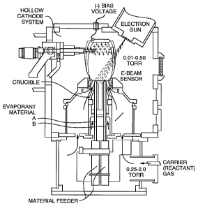
Example No. 1:
FIGS. 6-7 are schematic drawings representing an exemplary embodiment of the
present invention, wherein FIG. 7 illustrates an enlarged partial view of the
embodiment
of FIG. 6.
The invention may be embodied in other specific forms without departing from
the spirit or essential characteristics thereof. Of course, it should be
understood that a
wide range of changes and modifications can be made to the preferred
embodiment
described above. The foregoing embodiments are therefore to be considered in
all
respects illustrative rather than limiting of the invention described herein.
Scope of the
invention is thus indicated by the appended claims as read in light of the
foregoing
description, including all equivalents, and all changes which come within the
meaning
and range of equivalency of the claims are therefore intended to be embraced
herein.
-18-